Order
Now
Product
Folder
Support &
Community
Tools &
Software
Technical
Documents
TPS7A63-Q1, TPS7A6401-Q1
SLVSAB1G – JUNE 2011 – REVISED MARCH 2020
TPS7A63-Q1, TPS7A6401-Q1
300-mA, 40-V, Low-Dropout Regulator With Ultra-Low IQ
1 Features
2 Applications
•
•
•
•
•
1
•
•
•
•
•
•
•
•
•
•
•
AEC-Q100 qualified for automotive applications:
– Temperature grade 1: –40°C to 125°C, TA
– Junction Temperature: –40°C to 150°C, TJ
Low dropout voltage:
– 300 mV at IOUT = 150 mA
7-V to 40-V wide input-voltage range with up to
45-V transients
300-mA maximum output current
Ultralow quiescent current:
– IQUIESCENT = 35 µA (typical) at light loads
– ISLEEP < 2 µA when EN = low
Fixed (3.3-V and 5-V) and adjustable (2.5-V to
7-V) output voltages
Integrated watchdog with fault/flag
Stable with low-ESR ceramic output capacitor
Integrated power-on reset:
– Programmable delay
– Open-drain reset output
Integrated fault protection:
– Short-circuit and overcurrent protection
– Thermal shutdown
Low input-voltage tracking
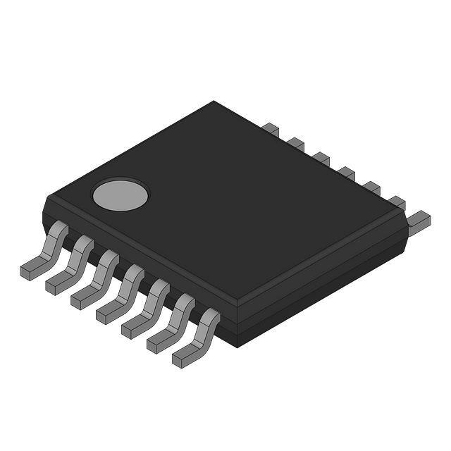
Thermally enhanced 14-pin HTSSOP-PWP
package and 10-pin VSON-DRK package
Automotive head units
Headlights
DC/DC converters
Automotive center information displays
3 Description
The TPS7A63-Q1 and TPS7A6401-Q1 are a family of
low-dropout linear voltage regulators designed for low
power consumption and quiescent current less than
35 µA in light-load applications. These devices,
designed to achieve stable operation even with a lowESR ceramic output capacitor, feature an integrated
programmable window watchdog and overcurrent
protection. Designers can program the output voltage
using external resistors. A low-voltage tracking
feature allows for a smaller input capacitor and can
possibly eliminate the need of using a boost
converter during cold-crank conditions. The poweron-reset delay is fixed (250 µs typical), or an external
capacitor can program the delay. Because of such
features, these devices are well-suited in power
supplies for various automotive applications.
Device Information(1)
PART NUMBER
PACKAGE
BODY SIZE (NOM)
TPS7A63-Q1,
TPS7A6401-Q1
HTSSOP (14)
5.00 mm × 4.40 mm
TPS7A63-Q1
VSON (10)
4.00 mm × 3.00 mm
(1) For all available packages, see the orderable addendum at
the end of the data sheet.
Fixed Output Voltage Option
VIN
VIN
CIN
TPS7A6x01-Q1
TPS7A6333-Q1
VOUT
or
TPS7A6350-Q1
RDELAY
Adjustable Output Voltage Option
VOUT
COUT
VIN
VOUT
VIN
CIN
FB
RDELAY
RRST
CDLY
ROSC
RRST
R2
CDLY
ROSC
ROSC
RESET
nRST
ROSC
nWD_EN
WD_FLT/
WD_FLG
WD
RESET
nRST
RFLT/FLAG
GND
EN
VOUT
COUT
R1
RFLT/FLAG
FAULT/
FLAG
GND
EN
nWD_EN
WD_FLT/
WD_FLG
WD
FAULT/
FLAG
1
An IMPORTANT NOTICE at the end of this data sheet addresses availability, warranty, changes, use in safety-critical applications,
intellectual property matters and other important disclaimers. PRODUCTION DATA.
�TPS7A63-Q1, TPS7A6401-Q1
SLVSAB1G – JUNE 2011 – REVISED MARCH 2020
www.ti.com
Table of Contents
1
2
3
4
5
6
7
Features ..................................................................
Applications ...........................................................
Description .............................................................
Revision History.....................................................
Pin Configuration and Functions .........................
Specifications.........................................................
1
1
1
2
4
5
6.1
6.2
6.3
6.4
6.5
6.6
5
5
5
6
6
8
Absolute Maximum Ratings ......................................
ESD Ratings..............................................................
Recommended Operating Conditions.......................
Thermal Information ..................................................
Electrical Characteristics...........................................
Typical Characteristics ..............................................
Detailed Description ............................................ 10
7.1 Overview ................................................................. 10
7.2 Functional Block Diagrams ..................................... 10
7.3 Feature Description................................................. 12
7.4 Device Functional Modes........................................ 20
8
Application and Implementation ........................ 21
8.1 Application Information............................................ 21
8.2 Typical Applications ............................................... 21
9 Power Supply Recommendations...................... 24
10 Layout................................................................... 24
10.1 Layout Guidelines ................................................. 24
10.2 Layout Example .................................................... 27
11 Device and Documentation Support ................. 28
11.1
11.2
11.3
11.4
11.5
11.6
Related Links ........................................................
Receiving Notification of Documentation Updates
Community Resources..........................................
Trademarks ...........................................................
Electrostatic Discharge Caution ............................
Glossary ................................................................
28
28
28
28
28
28
12 Mechanical, Packaging, and Orderable
Information ........................................................... 28
4 Revision History
NOTE: Page numbers for previous revisions may differ from page numbers in the current version.
Changes from Revision F (June 2018) to Revision G
Page
•
Changed AEC-Q100 Features bullets to conform to new standard ...................................................................................... 1
•
Changed input voltage range from 11 V to 7 V throughout document .................................................................................. 1
•
Changed Applications section ............................................................................................................................................... 1
•
Added footnote to VIN row in Recommended Operating Conditions table ............................................................................. 5
•
Added footnote to VIN row in Electrical Characteristics table ................................................................................................. 6
Changes from Revision E (September 2015) to Revision F
Page
•
Changed device names to TPS7A63-Q1 TPS7A6401-Q1..................................................................................................... 1
•
Changed 4 V to 11 V in fourth Features bullet ...................................................................................................................... 1
•
Changed VIN, VEN parameter row in Recommended Operating Conditions table: separated VIN and VEN into different
rows, changed VIN minimum specification from 4 V to 11 V .................................................................................................. 5
•
Changed VIN minimum specification from VOUT + 0.3 V to 11 V in Electrical Characteristics table ....................................... 6
•
Changed 4 V to 11 V in Example values column of Input voltage range row of Design Parameters table ......................... 22
•
Changed 4 V to 11 V in Example values column of Input voltage range row of Design Parameters table ........................ 23
•
Changed 4 V to 11 V in first sentence of Power Supply Recommendations section .......................................................... 24
Changes from Revision D (July 2012) to Revision E
•
2
Page
Added ESD Ratings table, Feature Description section, Device Functional Modes, Application and Implementation
section, Power Supply Recommendations section, Layout section, Device and Documentation Support section, and
Mechanical, Packaging, and Orderable Information section ................................................................................................. 5
Submit Documentation Feedback
Copyright © 2011–2020, Texas Instruments Incorporated
Product Folder Links: TPS7A63-Q1 TPS7A6401-Q1
�TPS7A63-Q1, TPS7A6401-Q1
www.ti.com
SLVSAB1G – JUNE 2011 – REVISED MARCH 2020
Changes from Revision C (April 2012) to Revision D
Page
•
Corrected part number in numerous locations throughout the data sheet ............................................................................. 1
•
Added new bullets at top of Features list ............................................................................................................................... 1
•
Deleted the NO. column from the electrical tables ................................................................................................................. 5
•
Deleted two Typical Characteristics graphs ........................................................................................................................... 8
Changes from Revision B (December 2011) to Revision C
•
Page
Changed regulated output voltage (6.1), added text to the test conditions (10mA to 200mA, VIN = VOUT + 1V to 16V) ....... 6
Changes from Revision A (August 2011) to Revision B
•
Page
Deleted devices TPS7A64333-Q1 and TPSA6450-Q1 .......................................................................................................... 1
Changes from Original (June 2011) to Revision A
Page
•
Deleted the Ordering Information Table ................................................................................................................................. 4
•
Changed values for VIL and VIH in the Watchdog Enable Input (nWD_EN pin) section......................................................... 7
•
Changed values for VIL and VIH in the Watchdog Input Pulse (WD pin) section.................................................................... 7
Copyright © 2011–2020, Texas Instruments Incorporated
Product Folder Links: TPS7A63-Q1 TPS7A6401-Q1
Submit Documentation Feedback
3
�TPS7A63-Q1, TPS7A6401-Q1
SLVSAB1G – JUNE 2011 – REVISED MARCH 2020
www.ti.com
5 Pin Configuration and Functions
PWP Package
14-Pin HTSSOP With PowerPAD IC Package
Top View (Fixed Output Voltage Option)
VIN
nRST
NC
GND
EN
RDELAY
VOUT
1
2
3
4
5
6
7
14
13
12
11
10
9
8
PWP Package
14-Pin HTSSOP With PowerPAD IC Package
Top View (Adjustable Output Voltage Option)
ROSC
NC
nWD_EN
NC
WD
WD_FLT/FLAG
NC
VIN
nRST
FB
GND
EN
RDELAY
VOUT
1
2
3
4
5
6
7
14
13
12
11
10
9
8
ROSC
NC
nWD_EN
NC
WD
WD_FLT/FLAG
NC
DRK Package
10-Pin VSON With Exposed Thermal Pad
Top View (Fixed Output Voltage Option)
VIN
1
10
ROSC
nRST
2
9
nWD_EN
GND
3
8
RDELAY
EN
4
7
WD
VOUT
5
6
WD_FLT
Pin Functions
PIN
NAME
PWP
DRK
EN
5
4
FB
3
GND
4
NC
I/O
DESCRIPTION
I
Chip enable pin: This is a high-voltage-tolerant input pin with an internal pulldown. A high input to this pin
activates the device and turns the regulator ON. Connect this input to the VIN terminal for self-bias applications.
If this pin remains unconnected, the device stays disabled.
—
I
Feedback pin (only applicable for TPS7A6x01-Q1): Sense voltage for error amplifier
3
I/O
Ground pin: This is signal ground pin of the device.
3
—
—
Not connected (only applicable for TPS7A6333-Q1 and TPS7A6350-Q1)
NC
8
—
—
Not connected
NC
11
—
—
Not connected
NC
13
—
—
Not connected
nRST
2
2
O
Reset pin: This is an open-drain reset output pin with an external pullup resistor connected to the VOUT pin.
nWD_EN
12
9
I
Watchdog enable pin: A high input to this pin disables the watchdog, and vice versa. This is an active-low input
pin with an internal pulldown. Leaving this pin is unconnected and floating keeps the watchdog enabled. An
external microcontroller can pull this pin high momentarily to disable and reinitialize the watchdog.
RDELAY
6
8
O
Reset delay timer pin: This pin programs the reset delay timer using an external capacitor (CDLY) to ground.
ROSC
14
10
O
ROscillator pin: This pin programs the internal oscillator frequency (and hence the duration of the watchdog
window) by connecting an external resistor to ground.
WD
10
7
I
Watchdog service pin: This is an input pin to provide a service signal to the watchdog.
WD_FLAG
9
6
O
Watchdog flag pin (for TPS7A6401-Q1 only): This is an active-high latched fault (that is, flag) output pin with an
external pullup resistor connected to VOUT pin.
WD_FLT
9
6
O
Watchdog fault pin (for TPS7A63-Q1 only): This is an active-low fault output pin with an external pullup resistor
connected to the VOUT pin.
VIN
1
1
I
Input voltage pin: The unregulated input voltage is supplied to this pin. A bypass capacitor connected between
the VIN pin and GND pin dampens line transients on the input.
VOUT
7
5
O
Regulated output voltage pin: This is a regulated voltage output (VOUT = 3.3 V or 5 V or a programmed value) pin
with a limitation on maximum output current. For devices with adjustable output voltage (TPS7A6x01-Q1),
connecting an external resistor network programs the output voltage. In order to achieve stable operation and
prevent oscillation, connect an external output capacitor (COUT) with low ESR between this pin and GND pin.
4
Submit Documentation Feedback
Copyright © 2011–2020, Texas Instruments Incorporated
Product Folder Links: TPS7A63-Q1 TPS7A6401-Q1
�TPS7A63-Q1, TPS7A6401-Q1
www.ti.com
SLVSAB1G – JUNE 2011 – REVISED MARCH 2020
6 Specifications
6.1 Absolute Maximum Ratings
over operating free-air temperature range (unless otherwise noted) (1)
MAX
UNIT
VIN, VEN
Unregulated inputs (2) (3)
DESCRIPTION
45
V
VOUT
Regulated output
7
V
FB
Sense voltage for error amplifier (2)
7
V
ROSC
Constant-voltage reference (2)
7
V
nWD_EN,
WD,
WD_FLAG,
WD_FLT
Watchdog inputs and outputs (2)
7
V
nRST
Open-drain reset output (2)
7
V
RDELAY
Reset delay timer output (2)
7
V
TA
Operating ambient temperature
125
°C
Tstg
Storage temperature
150
°C
(1)
(2)
(3)
MIN
–65
Stresses beyond those listed under Absolute Maximum Ratings may cause permanent damage to the device. These are stress ratings
only, and functional operation of the device at these or any other conditions beyond those indicated under Recommended Operating
Conditions is not implied. Exposure to absolute-maximum-rated conditions for extended periods may affect device reliability. All voltage
values are with respect to GND.
Absolute negative voltage on these pins not to go below –0.3 V.
Absolute maximum voltage for duration less than 480 ms.
6.2 ESD Ratings
VALUE
V(ESD)
(1)
Electrostatic discharge
Human body model (HBM), per AEC Q100-002 (1)
±4000
Charged device model (CDM), per AEC Q100-011
±1500
UNIT
V
AEC Q100-002 indicates HBM stressing is done in accordance with the ANSI/ESDA/JEDEC JS-001 specification.
6.3 Recommended Operating Conditions
MIN
MAX
7 (1)
40
V
Enable pin voltage
4
40
V
Low voltage input or output
0
5.25
V
–40
150
°C
VIN
Unregulated input voltage
VEN
nRST, RDELAY, nWD_EN, WD_FLT
WD_FLAG (3), WD, FB (4)
(2)
,
TJ
(1)
(2)
(3)
(4)
Operating junction temperature range
UNIT
VIN can go down to 4 V for 130 ms or less and remain functional. If VIN is less than 7 V for longer than 130 ms, then some devices can
turn off until the input voltage rises above 7 V.
Applicable for TPS7A63-Q1 only
Applicable for TPS7A6401-Q1 only
Applicable for TPS7A6301-Q1 and TPS7A6401-Q1 only
Copyright © 2011–2020, Texas Instruments Incorporated
Product Folder Links: TPS7A63-Q1 TPS7A6401-Q1
Submit Documentation Feedback
5
�TPS7A63-Q1, TPS7A6401-Q1
SLVSAB1G – JUNE 2011 – REVISED MARCH 2020
www.ti.com
6.4 Thermal Information
THERMAL METRIC
TPS7A6401-Q1
TPS7A63-Q1
(1)
PWP (HTTSOP)
DRK (VSON)
14 PINS
10 PINS
UNIT
RθJA
Junction-to-ambient thermal resistance
46
36.5
°C/W
RθJC(top)
Junction-to-case (top) thermal resistance
32.6
36.6
°C/W
RθJB
Junction-to-board thermal resistance
27.4
11.6
°C/W
ψJT
Junction-to-top characterization parameter
1.2
0.5
°C/W
ψJB
Junction-to-board characterization parameter
27.2
11.7
°C/W
RθJC(bot)
Junction-to-case (bottom) thermal resistance
2.5
3.8
°C/W
(1)
For more information about traditional and new thermal metrics, see the Semiconductor and IC Package Thermal Metrics application
report.
6.5 Electrical Characteristics
VIN = 14 V, TJ = –40ºC to 150ºC (unless otherwise noted)
PARAMETER
TEST CONDITIONS
MIN
TYP
MAX
UNIT
INPUT VOLTAGE (VIN PIN)
VIN
7 (1)
Input voltage
VOUT = 2.5 V to 7 V, IOUT = 1 mA
IQUIESCENT
Quiescent current
VIN = 8.2 V to 18 V, VEN = 5 V,
IOUT = 0.01 mA to 0.75 mA
40
ISLEEP
Sleep or shutdown current
VIN = 8.2 V to 18 V, VEN < 0.8 V,
IOUT = 0 mA (no load), TA = 125°C
VIN-UVLO
Undervoltage lockout
voltage
Ramp VIN down until output is turned OFF
3.16
V
VIN(POWERUP)
Power-up voltage
Ramp VIN up until output is turned ON
3.45
V
35
V
µA
3
µA
DEVICE ENABLE INPUT (EN PIN)
VIL
Logic-input low level
VIH
Logic-input high level
0
0.8
V
2.5
40
V
–2%
2%
REGULATED OUTPUT VOLTAGE (VOUT PIN)
Fixed VOUT value (3.3 V, 5 V or a programmed value),
IOUT = 10 mA to 200 mA, VIN = VOUT + 1 V to 16 V
VOUT
Regulated output voltage
ΔVLINE-REG
Line regulation
ΔVLOAD-REG
Load regulation
VDROPOUT
Dropout voltage
(VIN – VOUT)
IOUT = 200 mA
500
IOUT = 150 mA
300
RSW (2)
Switch resistance
VIN to VOUT resistance
IOUT
Output current
ICL
Output current limit
PSRR (4)
(1)
(2)
(3)
(4)
6
Power-supply ripple
rejection
VIN = 6 V to 28 V, IOUT = 10 mA, VOUT = 5 V
15
VIN = 6 V to 28 V, IOUT = 10 mA, VOUT = 3.3 V
20
IOUT = 10 mA to 200 mA, VIN = 14 V, VOUT = 5 V
25
IOUT = 10 mA to 200 mA, VIN = 14 V, VOUT = 3.3 V
35
2
VOUT in regulation
0
200
[VOUT in regulation, VOUT = 3.3 V, VIN = 6 V] (3)
0
300
350
1000
VOUT = 0 V (VOUT pin is shorted to ground)
VIN-RIPPLE = 0.5 Vpp, IOUT = 200 mA,
frequency = 100 Hz, VOUT = 5 V and VOUT = 3.3 V
60
VIN-RIPPLE = 0.5 Vpp, IOUT = 200 mA,
frequency = 150 kHz, VOUT = 5 V and VOUT = 3.3 V
30
mV
mV
mV
Ω
mA
mA
dB
VIN can go down to 4 V for 130 ms or less and remain functional. If VIN is less than 7 V for longer than 130 ms, then some devices can
turn off until the input voltage rises above 7 V.
This test is done with VOUT in regulation, measuring the VIN – VOUT parameter when VOUT drops by 100 mV from the programmed value
(of VOUT) at specified loads.
Design Information - not tested; specified by characterization.
Specified by design - not tested.
Submit Documentation Feedback
Copyright © 2011–2020, Texas Instruments Incorporated
Product Folder Links: TPS7A63-Q1 TPS7A6401-Q1
�TPS7A63-Q1, TPS7A6401-Q1
www.ti.com
SLVSAB1G – JUNE 2011 – REVISED MARCH 2020
Electrical Characteristics (continued)
VIN = 14 V, TJ = –40ºC to 150ºC (unless otherwise noted)
PARAMETER
TEST CONDITIONS
MIN
TYP
MAX
UNIT
RESET (nRST PIN)
VOL
Reset pulled low
IOL = 5 mA
IOH
Leakage current
Reset pulled to VOUT through a 5-kΩ resistor
VTH(POR)
Power-on-reset threshold
UVTHRES
VOUT powered up above internally set tolerance,
VOUT = 5 V
Power-on-reset delay
tPOR-PRESET
Internally preset
Power-on-reset delay
tDEGLITCH
Reset deglitch time
4.65
V
1
µA
4.77
V
VOUT powered up above internally set tolerance,
VOUT = 3.3 V
3.07
VOUT falling below internally set tolerance,
VOUT = 5 V
Reset threshold
tPOR (3)
4.5
0.4
4.5
4.65
4.77
V
VOUT falling below internally set tolerance,
VOUT = 3.3 V
3.07
CDLY = 100 pF
300
µs
CDLY = 100 nF
300
ms
CDLY not connected, VOUT = 5 V and VOUT = 3.3 V
250
µs
5.5
µs
RESET DELAY (RDELAY PIN)
VTH(RDELAY)
Threshold to release nRST
high
IDLY
Delay capacitor
charging current
IOL
Delay capacitor
discharging current
Voltage at RDELAY pin is ramped up
0.75
Voltage at RDELAY pin = 1 V
3
3.3
V
1
1.25
µA
5
mA
CURRENT VOLTAGE REFERENCE (ROSC PIN)
VROSC
Voltage reference
0.95
1
1.05
V
0.4
V
1
µA
0.8
V
WATCHDOG FAULT / FLAG OUTPUT (WD_FLT / WD_FLAG Pin)
VOL
IOH
Logic output low level
IOL= 5 mA
Leakage current
WD_FLT/WD_FLG pulled to VOUT through 5-kΩ
resistor
WATCHDOG ENABLE INPUT (nWD_EN PIN)
VIL
Logic input low level
VIH
Logic input high level
3 V < VDD < 5.25 V
2.5
3 V < VDD < 5.25 V
2.5
V
WATCHDOG INPUT PULSE (WD PIN)
VIL
Logic input low level
VIH
Logic input high level
0.8
tWD
Watchdog window duration
tWD-tol
Tolerance of watchdog
period using external
resistor
Excludes tolerance of ROSC
(external resistor connected to ROSC pin)
tWD-DEFAULT
Default watchdog period
External resistor not connected, ROSC pin is floating
or open
tWD-HOLD
Minimum pulse width for
resetting watch dog timer
V
ROSC = 10 kΩ ± 1%
10
ROSC = 20kΩ ± 1%
20
–10%
108
V
ms
10%
164
254
1.65
ms
µs
OPERATING TEMPERATURE RANGE
TJ
Operating junction
temperature
TSHUTDOWN
Thermal shutdown trip
point
THYST
Thermal shutdown
hysteresis
–40
Copyright © 2011–2020, Texas Instruments Incorporated
Product Folder Links: TPS7A63-Q1 TPS7A6401-Q1
150
ºC
165
ºC
10
ºC
Submit Documentation Feedback
7
�TPS7A63-Q1, TPS7A6401-Q1
SLVSAB1G – JUNE 2011 – REVISED MARCH 2020
www.ti.com
6.6 Typical Characteristics
55
60
IOUT = 1mA
50
VIN =14V
45
IQUIESCENT (µA)
I QUIESCENT (µA)
50
40
30
VIN = 14V
TA = 25°C
VOUT = 5V, 3.3V
20
35
30
25
20
15
10
0.1
1
10
VOUT = 5V, 3.3V
40
100
-50
0
50
T A (°C)
IOUT (mA)
Figure 1. Quiescent Current vs Load Current
0.4
V OUT = 5V
VOUT = 5V, 3.3V
0.35
TA= 25°C
0.3
500
VDROP OUT (V)
I QUIESCENT (µA)
600
400
300
IOUT = 100mA
200
0.25
T A = 125°C
0.2
T A = 25°C
0.15
T A = -40°C
0.1
No Load
100
0.05
0
4
14
24
V IN (V)
34
40
Figure 3. Quiescent Current vs Input Voltage
5.1
0
50
100
IOUT (mA)
150
200
Measure dropout voltage when the output voltage drops by 100 mV
from the regulated output-voltage level. (For example, for an output
voltage programmed to be 5 V, measure the dropout voltage when
the output voltage drops down to 4.9 V from 5 V.)
Figure 4. Dropout Voltage vs Load Current
6
VIN = 14V
5.08
IOUT = 1mA
IOUT = 100mA
TA = 25°C
5
5.06
5.04
4
5.02
VOUT (V)
VOUT (V)
150
Figure 2. Quiescent Current vs Ambient Air Temperature
700
0
100
5
4.98
3
2
4.96
4.94
1
4.92
4.9
-50
0
50
TA (°C)
100
150
Submit Documentation Feedback
2
3
4
5
6
7
V IN (V)
Figure 5. Output Voltage vs Ambient Air Temperature (VOUT
Set To 5 V)
8
0
Figure 6. Output Voltage vs Input Voltage
(VOUT Set To 5 V)
Copyright © 2011–2020, Texas Instruments Incorporated
Product Folder Links: TPS7A63-Q1 TPS7A6401-Q1
�TPS7A63-Q1, TPS7A6401-Q1
www.ti.com
SLVSAB1G – JUNE 2011 – REVISED MARCH 2020
Typical Characteristics (continued)
0.12
0.1
0.08
650
TA= 125°C
TA = 25°C
0.06
TA = -40°C
0.04
500
0
0
10
20
30
40
450
-50
50
VIN (V)
50
TA (°C)
Figure 7. Output Voltage vs Input Voltage
Figure 8. Output Current Limit vs Ambient Air Temperature
12
10.5
10
9.5
9
150
2
1.5
1
0.5
8.5
8
-50
0
50
T A (°C)
100
120
VIN = 14V
IOUT = 200mA
TA = 25°C
COUT = 10µF
VOUT = 5V, 3.3V
100
60
0
50
T A (°C)
100
150
Figure 10. Line Regulation vs Ambient Air Temperature
120
VIN = 14V
IOUT = 1mA
TA = 25°C
COUT = 10µF
VOUT = 5V, 3.3V
100
PSRR (dB)
80
0
-50
150
Figure 9. Load Regulation vs Ambient Air Temperature
PSRR (dB)
100
IOUT = 10mA
VOUT = 5V, 3.3V
VIN step from
8V to 28V
2.5
Line Regulation (mV)
11
0
3
VIN = 14V
VOUT = 5V, 3.3V
IOUT step from
10mA to 200mA
11.5
Load Regulation (mV)
600
550
0.02
80
60
40
40
20
20
0
VIN = 14V
VOUT = 5V, 3.3V
700
ICL (mA)
IOUT (A)
750
ILOAD = 100mA
VOUT = 5V, 3.3V
0
10
100
10k
1k
Frequency (Hz)
100k
1M
Figure 11. PSRR at Heavy Load Current
10
100
10k
1k
Frequency (Hz)
100k
1M
Figure 12. PSRR at Light Load Current
Copyright © 2011–2020, Texas Instruments Incorporated
Product Folder Links: TPS7A63-Q1 TPS7A6401-Q1
Submit Documentation Feedback
9
�TPS7A63-Q1, TPS7A6401-Q1
SLVSAB1G – JUNE 2011 – REVISED MARCH 2020
www.ti.com
7 Detailed Description
7.1 Overview
The TPS7A63-Q1 and TPS7A6401-Q1 are a family of monolithic low-dropout linear voltage regulators with
integrated watchdog and reset functionality. These voltage regulators are designed for low power consumption
and quiescent current less than 25 µA in light-load applications. Because of a programmable reset delay (also
called power-on-reset delay), these devices are well-suited in power supplies for microprocessors and
microcontrollers.
These devices are available in two fixed and adjustable output-voltage versions as follows:
• Fault (WD_FLT) output version: TPS7A63-Q1
• Flag (WD_FLAG) output version: TPS7A6401-Q1
Feature Description describes the features of the TPS7A63-Q1 and TPS7A6401-Q1 voltage regulators in detail.
7.2 Functional Block Diagrams
VIN
Band Gap
VRef1
VIN
CIN
Temp. Sensor/
Thermal Shutdown
UVLO Comp.
with internal
reference
Q1
VRef1
EN
Regulator
Control
Logic
Control
Error
Amp.
VOUT
VOUT
Over
Current
Detection
RDELAY
CDLY
Charge Pump
Oscillator
COUT
RRST
Voltage
Supervisor with
Reset Delay
Q2
RESET
nRST
ROSC
Current
Regulator
ROSC
Watchdog
Oscillator
RFLT
Timer
WD_FLT
Q3
GND
FAULT
Watchdog
Fault Control
nWD_EN
WD
Figure 13. TPS7A6333-Q1 and TPS7A6350-Q1 (Fixed Output Voltage With Fault Output)
10
Submit Documentation Feedback
Copyright © 2011–2020, Texas Instruments Incorporated
Product Folder Links: TPS7A63-Q1 TPS7A6401-Q1
�TPS7A63-Q1, TPS7A6401-Q1
www.ti.com
SLVSAB1G – JUNE 2011 – REVISED MARCH 2020
Functional Block Diagrams (continued)
VIN
Band Gap
VRef1
Temp. Sensor/
Thermal Shutdown
VIN
CIN
UVLO Comp.
with internal
reference
Q1
VRef1
EN
Regulator
Control
Logic
Control
Error
Amp.
VOUT
VOUT
FB
R2
Over Current
Detection
RDELAY
COUT
R1
RRST
Voltage
Supervisor with
Reset Delay
CDLY
Charge Pump
Oscillator
Q2
RESET
nRST
ROSC
Current
Regulator
ROSC
Watchdog
Oscillator
RFLT
Timer
WD_FLT
Q3
GND
FAULT
Watchdog
Fault Control
nWD_EN
WD
Figure 14. TPS7A6301 (Adjustable Output Voltage With Fault Output)
VIN
Band Gap
VRef1
VIN
CIN
Temp. Sensor/
Thermal Shutdown
UVLO Comp.
with internal
reference
Q1
VRef1
EN
Regulator
Control
Logic
Control
Error
Amp.
VOUT
VOUT
FB
R2
Over Current
Detection
RDELAY
COUT
R1
RRST
Voltage
Supervisor with
Reset Delay
CDLY
Charge Pump
Oscillator
Current
Regulator
Watchdog
Oscillator
Q2
RESET
nRST
ROSC
ROSC
RFLAG
Timer
WD_FLAG
Q3
GND
FLAG
Watchdog
Fault Control
nWD_EN
WD
Figure 15. TPS7A6401-Q1 (Adjustable Output Voltage With Flag Output)
Copyright © 2011–2020, Texas Instruments Incorporated
Product Folder Links: TPS7A63-Q1 TPS7A6401-Q1
Submit Documentation Feedback
11
�TPS7A63-Q1, TPS7A6401-Q1
SLVSAB1G – JUNE 2011 – REVISED MARCH 2020
www.ti.com
7.3 Feature Description
7.3.1 Power Up, Reset Delay, and Reset Output
During power up, the regulator incorporates a protection scheme to limit the current through the pass element
and output capacitor. When the input voltage exceeds a certain threshold (VIN(POWERUP)) level, the output voltage
begins to ramp up as shown in Figure 16.
When starting up, and also when the output recovers from a negative voltage spike due to a load step or a dip in
the input voltage for a specified duration, the device implements reset delay to indicate that output voltage is
stable and in regulation.
When the output voltage reaches the power-on-reset threshold (VTH(POR)) level, that is, 93% of regulated output
voltage (3.3 V or 5 V, or a programmed value), a constant output current charges an external capacitor (CDLY) to
an internal threshold (VTH(RDELAY)) voltage level. Then, nRST asserts high and CDLY discharges through an
internal load. This allows CDLY to charge from approximately 0 V during the next power cycle.
Program the reset delay time by connecting an external capacitor (CDLY ,100 pF to 100 nF) to the RDELAY pin.
Equation 1 gives the delay time:
tPOR =
CDLY ´ 3
1´ 10-6
where
•
•
tPOR = reset delay time in seconds
CDLY = reset delay capacitor value in farads
(1)
VIN(POWERUP)
VIN t < tDEGLITCH
0
0
t>tDEGLITCH
VIN
VTH(POR)
VTH(POR)= 93% of VOUT
UVTHRES
0
0
VOUT
VOUT
VTH(RDELAY)
0
VTH(RDELAY)
0
VRDELAY
tPOR
VRDELAY
tDEGLITCH
tPOR
VnRST
VnRST
0
0
Figure 16. Power Up and Conditions for Activation
of Reset
Figure 17. Reset Delay and Deglitch Filter
As Figure 17 shows, if the regulated output voltage falls below 93% of the set level, nRST asserts low after a
short de-glitch time of approximately 5.5 µs (typical). In case of negative transients in the input voltage (VIN), the
reset signal asserts low only if the output (VOUT) drops and stays below the reset threshold level (VTH(POR)) for
more than the deglitch time (tDEGLITCH), as Figure 17 and Figure 20 illustrate. While nRST is low, if the input
voltage returns to the nominal operating voltage, the normal power-up sequence ensues. nRST asserts high only
if the output voltage exceeds the reset threshold voltage (VTH(POR)) and the reset delay time (tPOR) has elapsed.
12
Submit Documentation Feedback
Copyright © 2011–2020, Texas Instruments Incorporated
Product Folder Links: TPS7A63-Q1 TPS7A6401-Q1
�TPS7A63-Q1, TPS7A6401-Q1
www.ti.com
SLVSAB1G – JUNE 2011 – REVISED MARCH 2020
Feature Description (continued)
7.3.2 Adjustable Output Voltage
Program the regulated output voltage (VOUT) by connecting external resistors to FB pin. Calculate the feedback
resistor values using Equation 2.
R1 ù
é
VOUT = VREF ê1 +
R2 úû
ë
where
•
•
•
VOUT= desired output voltage
VREF = reference voltage (VREF= 1.23 V, typically)
R1, R2 = feedback resistors (see Figure 15)
(2)
Equation 3 gives the overall tolerance of the regulated output.
é R1 ù
tolVOUT = tolVREF + ê
ú éë tolR1 + tolR2 ùû
ë R1 + R2 û
where
•
•
•
tolVOUT = tolerance of the output voltage
tolVREF = tolerance of the internal reference voltage (tolVREF = ± 1.5% typically)
tolR1,tolR2 = tolerance of feedback resistors R1, R2
(3)
For a tighter tolerance on VOUT, select lower-value feedback resistors. TI recommends to select feedback
resistors such that the sum of R1 and R2 is from 20 kΩ to 200 kΩ.
7.3.3 Chip Enable
These devices have a high-voltage-tolerant EN pin that an external microcontroller or a digital control circuit can
use to enable and disable them. A high input to this pin activates the device and turns the regulator on. For self
bias applications, connect this input to the VIN terminal. An internal pulldown resistor is connected to this pin,
and therefore if this pin remains unconnected, the device stays disabled.
7.3.4 Charge Pump Operation
Charge Pump State
Charge Pump State
These devices have an internal charge pump which turns on or off depending on the input voltage and the output
current. The charge pump switching circuitry must not cause conducted emissions to exceed required thresholds
on the input voltage line. For a given output current, the charge pump stays on at lower input voltages and turns
off at higher input voltages. The charge pump switching thresholds are hysteretic. Figure 18 and Figure 19 show
typical switching thresholds for the charge pump at light (IOUT < approximately 2 mA) and heavy (IOUT >
approximately 2 mA) loads, respectively.
ON
Hysteresis
OFF
7.8
ON
Hysteresis
OFF
9.2
7.9
9.6
VIN (V)
VIN (V)
Figure 18. Charge Pump Operation at Light
Loads
Figure 19. Charge Pump Operation at Heavy
Loads
Copyright © 2011–2020, Texas Instruments Incorporated
Product Folder Links: TPS7A63-Q1 TPS7A6401-Q1
Submit Documentation Feedback
13
�TPS7A63-Q1, TPS7A6401-Q1
SLVSAB1G – JUNE 2011 – REVISED MARCH 2020
www.ti.com
7.3.5 Low-Power Mode
At light loads and high input voltages (VIN > approximately 8 V, such that the charge pump is off), the device
operates in low-power mode and the quiescent current consumption is reduced to 25 µA (typical) as shown in
Table 1.
Table 1. Typical Quiescent Current Consumption
IOUT
Charge Pump ON
Charge Pump OFF
IOUT < approximately 2 mA
(Light load)
250 µA
35 µA
(Low-power mode)
IOUT > approximately 2 mA
(Heavy load)
280 µA
70 µA
7.3.6 Undervoltage Shutdown
These devices have an integrated undervoltage lockout (UVLO) circuit to shut down the output if the input
voltage (VIN) falls below an internally fixed UVLO threshold level (VIN-UVLO). This ensures that the regulator does
not latch into an unknown state during low input voltage conditions. The regulator powers up when the input
voltage exceeds the VIN(POWERUP) level, as Figure 20 shows.
7.3.7 Low-Voltage Tracking
At low input voltages, the regulator drops out of regulation, and the output voltage tracks the input minus a
voltage based on the load current (IOUT) and switch resistance (RSW), as Figure 20 shows. This feature allows for
a smaller input capacitor and can possibly eliminate the need of using a boost convertor during cold crank
conditions, as Figure 20 shows.
7.3.8 Integrated Fault Protection
These devices feature integrated fault protection to make them ideal for use in automotive applications. In order
to remain in a safe area of operation during certain fault conditions, the devices use internal current-limit
protection and current-limit foldback to limit the maximum output current. This protects them from excessive
power dissipation. For example, during a short-circuit condition on the output, fault protection limits the current
through the pass element to ICL to protect the device from excessive power dissipation.
7.3.9 Thermal Shutdown
These devices incorporate a thermal shutdown (TSD) circuit as a protection from overheating. For continuous
normal operation, the junction temperature should not exceed the TSD trip point. The junction temperature
exceeding the TSD trip point causes the output to turn off. When the junction temperature falls below TSD trip
point, the output turns on again, as Figure 21 shows.
14
Submit Documentation Feedback
Copyright © 2011–2020, Texas Instruments Incorporated
Product Folder Links: TPS7A63-Q1 TPS7A6401-Q1
�TPS7A63-Q1, TPS7A6401-Q1
www.ti.com
SLVSAB1G – JUNE 2011 – REVISED MARCH 2020
Tracking
VIN-UVLO
VIN
0
UVTHRES
0
VOUT
0
VRDELAY
tDEGLITCH
VnRST
0
Figure 20. Low-Voltage Tracking and Undervoltage
Lockout
Figure 21. Thermal Cycling Waveform for
TPS7A6350-Q1 (VIN= 24 V, IOUT= 200 mA, VOUT= 5 V)
7.3.10 Integrated Window Watchdog
These devices have an integrated watchdog with fault (WD_FLT) and flag (WD_FLAG) output options. Both
device options are available in fixed- and adjustable-output versions. The watchdog operation, service fault
conditions, and difference between fault (TPS7A63-Q1) and flag (TPS7A6401-Q1) output versions are described
as follows.
7.3.10.1 Programmable-Window Watchdog
Program the duration of the watchdog window by connecting an external resistor (ROSC) to ground at the ROSC
pin. The current through the resistor sets the clock frequency of the internal oscillator. The user can adjust the
duration of the watchdog window (that is, the watchdog timer period) by changing the resistor value. The duration
of the watchdog window and the duration of the fault output are multiples of the internal oscillator frequency and
are given by the following equations:
tWD = 10–6 × ROSC = 5000 × 1 / fOSC
tWD_OUT = 1 / fOSC
tCW = tOW = 1 / 2 tWD
(4)
(5)
where
•
•
•
•
•
•
tWD = width of watchdog window
ROSC = resistor connected at ROSC pin
tWD_OUT = duration of fault output
fOSC = frequency of internal oscillator
tCW = duration of closed window
tOW = duration of open window
(6)
As shown in Figure 22, each watchdog window consists of an open window and a closed window, each having a
width approximately 50% of the watchdog window. However, there is an exception to this; the first open window
after watchdog initialization is eight times the duration of the watchdog window. All open windows except the one
after watchdog initialization are one-half the width of the watchdog window. On initialization, the watchdog must
receive service (by software, external microcontroller, and so forth) only during an open window. A watchdog
serviced during a closed window, or not serviced during a open window, creates a watchdog fault condition.
Copyright © 2011–2020, Texas Instruments Incorporated
Product Folder Links: TPS7A63-Q1 TPS7A6401-Q1
Submit Documentation Feedback
15
�TPS7A63-Q1, TPS7A6401-Q1
SLVSAB1G – JUNE 2011 – REVISED MARCH 2020
www.ti.com
CLOSED
OPEN
After watchdog initialization
(must be serviced to prevent fault)
WINDOW
(must not be serviced
to prevent fault)
WINDOW
(must be serviced to
prevent fault)
8 x tWD
tCW=½ tWD
tOW=½ tWD
OPEN WINDOW
Event causing
watchdog initialization
tWD = 5000 x tWD_OUT
Figure 22. Watchdog Window Duration
7.3.10.2 Watchdog Enable
An external microcontroller or a digital circuit can apply an appropriate signal to the nWD_EN pin to enable or
disable the watchdog. A low input to this pin turns the watchdog on. Because of an internal pulldown resistor
connected to this pin, leaving the pin unconnected keeps the watchdog enabled.
7.3.10.3 Watchdog Service Signal
In order for the watchdog service signal (WD) to service an open window correctly, the service signal must stay
high for a duration of at least tWD_HOLD. The recommended value of tWD_HOLD is given by Equation 7:
tWD_HOLD = 3 × tWD_OUT
(7)
7.3.10.4 Watchdog Fault Outputs
The WD_FLT pin and WD_FLAG pin are fault output terminals for the TPS7A63-Q1 and TPS7A6401-Q1
devices, respectively. Typically, one pulls these fault outputs high to a regulated output supply. In the case of a
watchdog fault condition, the TPS7A63-Q1 momentarily pulls WD_FLT low for a duration of tWD_OUT, whereas the
TPS7A6401-Q1 latches the WD_FLAG high and momentarily pulls nRST low for a duration of tWD_OUT.
7.3.10.5 Watchdog Initialization
On power up and during normal operation, the watchdog initializes under the conditions shown in Table 2. The
normal operation of the watchdog for the WD_FLT and WD_FLAG output device options is shown in Figure 23
and Figure 24, respectively.
Table 2. Conditions For Watchdog Initialization
Edge
16
TPS7A63-Q1
(FAULT Option)
TPS7A6401-Q1
(FLAG Option)
Rising edge of nRST (when VOUT exceeds VTH(POR)) while
the watchdog is in the enabled state, for example, during
soft power up
✓
✓
Falling edge of nWD_EN while the nRST is already high,
for example, when the microprocessor enables the
watchdog after the device is powered up
✓
✓
Rising edge of WD_FLT while the nRST is already high
and the watchdog is in the enabled state, for example, right
after a closed window is serviced
✓
X
What causes watchdog to initialize?
Submit Documentation Feedback
Copyright © 2011–2020, Texas Instruments Incorporated
Product Folder Links: TPS7A63-Q1 TPS7A6401-Q1
�TPS7A63-Q1, TPS7A6401-Q1
www.ti.com
SLVSAB1G – JUNE 2011 – REVISED MARCH 2020
7.3.10.6 Watchdog Operation
tPOR
tPOR
93% of VOUT
93% of VOUT
0
0
VOUT
VOUT
0
0
nRST
nRST
0
0
tWD_HOLD
nWD_EN
0
tWD_HOLD
nWD_EN
0
WD
WD
0
0
WD_FLT
WD
Window
Status
WD_FLAG
NA
OW
WD Initialization
CW
OW