Sample &
Buy
Product
Folder
Support &
Community
Tools &
Software
Technical
Documents
TPS7A8101
SBVS179B – DECEMBER 2011 – REVISED AUGUST 2015
TPS7A8101 Low-Noise, Wide-Bandwidth, High PSRR,
Low-Dropout 1-A Linear Regulator
1 Features
3 Description
•
•
•
The TPS7A8101 low-dropout linear regulator (LDO)
offers very good performance in noise and powersupply rejection ratio (PSRR) at the output. This LDO
uses an advanced BiCMOS process and a
PMOSFET pass device to achieve very low noise,
excellent transient response, and excellent PSRR
performance.
1
•
•
•
•
•
•
•
Low-Dropout 1-A Regulator with Enable
Adjustable Output Voltage: 0.8 V to 6 V
Wide-Bandwidth High PSRR:
– 80 dB at 1 kHz
– 60 dB at 100 kHz
– 54 dB at 1 MHz
Low Noise: 23.5 μVRMS typical (100 Hz to
100 kHz)
Stable with a 4.7-μF Capacitance
Excellent Load and Line Transient Response
3% Overall Accuracy (Over Load, Line,
Temperature)
Overcurrent and Overtemperature Protection
Very Low Dropout: 170 mV Typical at 1 A
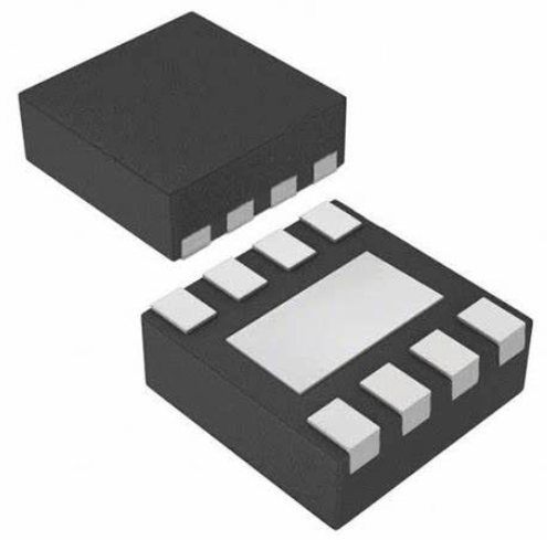
Package: 3-mm × 3-mm SON-8
The TPS7A8101 device is stable with a 4.7-μF
ceramic output capacitor, and uses a precision
voltage reference and feedback loop to achieve a
worst-case accuracy of 3% over all load, line,
process, and temperature variations.
This device is fully specified over the temperature
range of TJ = –40°C to 125°C and is offered in a 3mm × 3-mm, SON-8 package with a thermal pad.
Device Information(1)
PART NUMBER
2 Applications
•
•
•
PACKAGE
TPS7A8101
SON (8)
BODY SIZE (NOM)
3.00 mm × 3.00 mm
(1) For all available packages, see the orderable addendum at
the end of the data sheet.
Telecom Infrastructure
Audio
High-Speed I/F (PLL and VCO)
Typical Application Circuit
VIN
IN
CIN
VOUT
OUT
R1
TPS7A8101
EN
GND
FB
NR
CNR
R2
CBYPASS
COUT
VEN
1
An IMPORTANT NOTICE at the end of this data sheet addresses availability, warranty, changes, use in safety-critical applications,
intellectual property matters and other important disclaimers. PRODUCTION DATA.
�TPS7A8101
SBVS179B – DECEMBER 2011 – REVISED AUGUST 2015
www.ti.com
Table of Contents
1
2
3
4
5
6
7
1
1
1
2
3
4
9 Power Supply Recommendations...................... 15
10 Layout................................................................... 16
6.1
6.2
6.3
6.4
6.5
6.6
4
4
4
4
5
6
11 Device and Documentation Support ................. 19
Absolute Maximum Ratings ......................................
ESD Ratings..............................................................
Recommended Operating Conditions.......................
Thermal Information ..................................................
Electrical Characteristics...........................................
Typical Characteristics ..............................................
Detailed Description ............................................ 11
7.1
7.2
7.3
7.4
8
8.1 Application Information............................................ 13
8.2 Typical Application .................................................. 13
Features ..................................................................
Applications ...........................................................
Description .............................................................
Revision History.....................................................
Pin Configuration and Functions .........................
Specifications.........................................................
Overview .................................................................
Functional Block Diagram .......................................
Feature Description.................................................
Device Functional Modes........................................
11
11
11
12
Application and Implementation ........................ 13
10.1
10.2
10.3
10.4
10.5
11.1
11.2
11.3
11.4
11.5
11.6
Layout Guidelines .................................................
Layout Example ....................................................
Thermal Protection................................................
Power Dissipation .................................................
Estimating Junction Temperature ........................
Device Support......................................................
Documentation Support ........................................
Community Resources..........................................
Trademarks ...........................................................
Electrostatic Discharge Caution ............................
Glossary ................................................................
16
16
16
17
17
19
19
19
19
19
19
12 Mechanical, Packaging, and Orderable
Information ........................................................... 19
4 Revision History
NOTE: Page numbers for previous revisions may differ from page numbers in the current version.
Changes from Revision A (April 2012) to Revision B
•
Added ESD Ratings table, Feature Description section, Device Functional Modes, Application and Implementation
section, Power Supply Recommendations section, Layout section, Device and Documentation Support section, and
Mechanical, Packaging, and Orderable Information section ................................................................................................. 1
Changes from Original (December 2011) to Revision A
•
2
Page
Page
Added new footnote 2 to Thermal Information table, changed footnote 3 ............................................................................. 4
Submit Documentation Feedback
Copyright © 2011–2015, Texas Instruments Incorporated
Product Folder Links: TPS7A8101
�TPS7A8101
www.ti.com
SBVS179B – DECEMBER 2011 – REVISED AUGUST 2015
5 Pin Configuration and Functions
DRB PACKAGE
8-Pin SON With Exposed Thermal Pad
Top View
OUT
1
8
IN
OUT
2
7
IN
FB/SNS
3
6
NR
GND
4
5
EN
Pin Functions
PIN
NAME
EN
FB
GND
IN
NR
OUT
I/O
DESCRIPTION
I
Driving this pin high turns on the regulator. Driving this pin low puts the regulator into shutdown mode.
Refer to the Shutdown section for more details. EN must not be left floating and can be connected to IN
if not used.
3
I
This pin is the input to the control-loop error amplifier and is used to set the output voltage of the device.
4, pad
—
NO.
5
7
8
6
1
2
I
Ground
Unregulated input supply
—
Connect an external capacitor between this pin and ground to reduce output noise to very low levels.
The capacitor also slows down the VOUT ramp (RC softstart).
O
Regulator output. A 4.7-μF or larger capacitor of any type is required for stability.
Submit Documentation Feedback
Copyright © 2011–2015, Texas Instruments Incorporated
Product Folder Links: TPS7A8101
3
�TPS7A8101
SBVS179B – DECEMBER 2011 – REVISED AUGUST 2015
www.ti.com
6 Specifications
6.1 Absolute Maximum Ratings
Over operating free-air temperature range (unless otherwise noted). (1)
Voltage
Current
(2)
MAX
–0.3
7
FB, NR
–0.3
3.6
EN
–0.3
VIN + 0.3 (2)
OUT
–0.3
7
OUT
Temperature
(1)
MIN
IN
UNIT
V
Internally Limited
A
Operating virtual junction, TJ
–55
150
°C
Storage, Tstg
–55
150
°C
Stresses beyond those listed under Absolute Maximum Ratings may cause permanent damage to the device. These are stress ratings
only, and functional operation of the device at these or any other conditions beyond those indicated is not implied. Exposure to absolutemaximum-rated conditions for extended periods my affect device reliability.
VEN absolute maximum rating is VIN + 0.3 V or +7 V, whichever is smaller.
6.2 ESD Ratings
VALUE
Human body model (HBM), per ANSI/ESDA/JEDEC JS-001, all pins
V(ESD)
(1)
(2)
Electrostatic discharge
(1)
UNIT
±2000
Charged device model (CDM), per JEDEC specification JESD22-C101, all
pins (2)
V
±500
JEDEC document JEP155 states that 500-V HBM allows safe manufacturing with a standard ESD control process.
JEDEC document JEP157 states that 250-V CDM allows safe manufacturing with a standard ESD control process.
6.3 Recommended Operating Conditions
Over operating free-air temperature range (unless otherwise noted)
VI
Input voltage
IO
Output current
TA
Operating free air temperature
MIN
MAX
2.2
6.5
UNIT
V
0
1
A
–40
125
°C
6.4 Thermal Information
TPS7A8101
THERMAL METRIC (1)
DRV (SON)
UNIT
8 PINS
RθJA
Junction-to-ambient thermal resistance
47.8
°C/W
RθJC(top)
Junction-to-case (top) thermal resistance
53.9
°C/W
RθJB
Junction-to-board thermal resistance
23.4
°C/W
ψJT
Junction-to-top characterization parameter
1
°C/W
ψJB
Junction-to-board characterization parameter
23.5
°C/W
RθJC(bot)
Junction-to-case (bottom) thermal resistance
7.4
°C/W
(1)
4
For more information about traditional and new thermal metrics, see the Semiconductor and IC Package Thermal Metrics application
report, SPRA953.
Submit Documentation Feedback
Copyright © 2011–2015, Texas Instruments Incorporated
Product Folder Links: TPS7A8101
�TPS7A8101
www.ti.com
SBVS179B – DECEMBER 2011 – REVISED AUGUST 2015
6.5 Electrical Characteristics
Over the operating temperature range of TJ = –40°C to +125°C, VIN = VOUT(TYP) + 0.5 V or 2.2 V (whichever is greater), IOUT =
1 mA, VEN = 2.2 V, COUT = 4.7 μF, CNR = 0.01 μF, and CBYPASS = 0 μF, unless otherwise noted. TPS7A8101 is tested at VOUT
= 0.8 V and VOUT = 6 V. Typical values are at TJ = 25°C.
PARAMETER
VIN
Input voltage range
VNR
Internal reference
TEST CONDITIONS
TYP
MAX
6.5
V
0.8
0.81
V
0.8
6
V
VOUT + 0.5 V ≤ VIN ≤ 6 V, VIN ≥ 2.5 V,
100 mA ≤ IOUT ≤ 500 mA, 0°C ≤ TJ ≤ 85°C
-2%
2%
VOUT + 0.5 V ≤ VIN ≤ 6.5 V, VIN ≥ 2.2 V,
100 mA ≤ IOUT ≤ 1 A
–3%
(1)
2.2
0.79
Output voltage range
VOUT
Output accuracy (2)
ΔVO(ΔVI)
Line regulation
VOUT(NOM) + 0.5 V ≤ VIN ≤ 6.5 V, VIN ≥ 2.2 V,
IOUT = 100 mA
ΔVO(ΔIL)
Load regulation
100 mA ≤ IOUT ≤ 1 A
Dropout voltage (3)
VDO
ILIM
Output current limit
350
VOUT + 0.5 V ≤ VIN ≤ 6.5 V, VIN ≥ 2.5 V,
IOUT = 1 A, VFB = GND or VSNS = GND
500
VEN ≤ 0.4 V, VIN ≥ 2.2 V, RL = 1 kΩ,
0°C ≤ TJ ≤ 85°C
IFB
Feedback pin current
VIN = 6.5 V, VFB = 0.8 V
VIN = 4.3 V, VOUT = 3.3 V,
IOUT = 750 mA
μA
2
μA
0.02
1
μA
f = 1 kHz
82
f = 10 kHz
78
f = 100 kHz
60
f = 1 MHz
54
BW = 100 Hz to 100 kHz,
VIN = 3.8 V, VOUT = 3.3 V,
IOUT = 100 mA, CNR = CBYPASS = 470 nF
VEN(LO)
Enable low (shutdown)
RL = 1 kΩ
IEN(HI)
Enable pin current, enabled
VIN = VEN = 6.5 V
tSTR
Start-up time
VOUT(NOM) = 3.3 V, VOUT = 0% to 90% VOUT(NOM),
RL = 3.3 kΩ, COUT = 10 μF, CNR = 470 nF
Undervoltage lockout
VIN rising, RL = 1 kΩ
Hysteresis
VIN falling, RL = 1 kΩ
(3)
mA
0.2
80
Enable high (enabled)
(1)
(2)
100
f = 100 Hz
VEN(HI)
Operating junction temperature
2000
60
mV
350
Output noise voltage
TJ
1400
IOUT = 1 A
Vn
Thermal shutdown temperature
1100
IOUT = 1 mA
Shutdown current (IGND)
TSD
μV/mA
VOUT + 0.5 V ≤ VIN ≤ 6.5 V, VIN ≥ 2.5 V,
IOUT = 750 mA, VFB = GND or VSNS = GND
ISHDN
UVLO
μV/V
150
250
VOUT = 0.85 × VOUT(NOM), VIN ≥ 3.3 V
UNIT
3%
2
Ground pin current
Power-supply rejection ratio
±0.3%
VOUT + 0.5 V ≤ VIN ≤ 6.5 V, VIN ≥ 2.2 V,
IOUT = 500 mA, VFB = GND or VSNS = GND
IGND
PSRR
MIN
dB
μVRMS
23.5
2.2 V ≤ VIN ≤ 3.6 V, RL = 1 kΩ
1.2
3.6 V < VIN ≤ 6.5 V, RL = 1 kΩ
1.35
V
0
0.02
0.4
V
1
μA
80
1.86
2
ms
2.10
V
75
mV
Shutdown, temperature increasing
160
°C
Reset, temperature decreasing
140
–40
°C
125
°C
Minimum VIN = VOUT + VDO or 2.2 V, whichever is greater.
The TPS7A8101 does not include external resistor tolerances and it is not tested at this condition: VOUT = 0.8 V, 4.5V ≤ VIN ≤ 6.5 V, and
750 mA ≤ IOUT ≤ 1 A because the power dissipation is greater than the maximum rating of the package.
VDO is not measured for fixed output voltage devices with VOUT < 1.7 V because minimum VIN = 2.2 V.
Submit Documentation Feedback
Copyright © 2011–2015, Texas Instruments Incorporated
Product Folder Links: TPS7A8101
5
�TPS7A8101
SBVS179B – DECEMBER 2011 – REVISED AUGUST 2015
www.ti.com
6.6 Typical Characteristics
At VOnom = 3.3 V, VI = VOnom + 0.5 V or 2.2 V (whichever is greater), IO = 100 mA, V(EN) = VI, C(IN) = 1 μF, C(OUT) = 4.7 μF, and C(NR) = 0.01
μF; all temperature values refer to TJ, unless otherwise noted.
3.399
3.399
125°C
85°C
25°C
0°C
–40°C
3.333
3.3
3.267
3.234
3.333
3.3
3.267
3.234
3.201
3.201
0
100 200 300 400 500 600 700 800 900 1000
Output Current (mA)
0
NOTE: The Y-axis shows 1% VO per division
Figure 1. Load Regulation
20
25
Figure 2. Load Regulation Under Light Loads
125°C
85°C
25°C
0°C
–40°C
Output Voltage (V)
0.818
125°C
85°C
25°C
0°C
–40°C
0.816
0.8
0.792
0.784
0.808
0.8
0.792
0.784
0.776
0.776
2.2
2.6
3
3.4
3.8 4.2 4.6 5
Input Voltage (V)
5.4
5.8
6.2
6.6
2.2
VO = 0.8 V
IO = 750 mA
NOTE: The Y-axis shows 1% VO per division
2.6
3
3.4
3.8 4.2 4.6 5
Input Voltage (V)
5.4
5.8
6.2
6.6
VO = 0.8 V
IO = 5 mA
NOTE: The Y-axis shows 1% VO per division
Figure 3. Line Regulation
Figure 4. Line Regulation Under Light Loads
500
500
125°C
85°C
25°C
0°C
–40°C
400
350
125°C
85°C
25°C
0°C
–40°C
450
400
Dropout Voltage (V)
450
Dropout Voltage (V)
10
15
Output Current (mA)
0.824
0.816
300
250
200
150
350
300
250
200
150
100
100
50
50
0
0
2
2.5
3
3.5
4
4.5
5
Input Voltage (V)
5.5
6
IO = 1 A
6.5
2
2.5
3
3.5
4
4.5
5
Input Voltage (V)
5.5
6
6.5
IO = 750 mA
Figure 5. Dropout Voltage vs Input Voltage
6
5
NOTE: The Y-axis shows 1% VO per division
0.824
Output Voltage (V)
125°C
85°C
25°C
0°C
–40°C
3.366
Output Voltage (V)
Output Voltage (V)
3.366
Figure 6. Dropout Voltage vs Input Voltage
Submit Documentation Feedback
Copyright © 2011–2015, Texas Instruments Incorporated
Product Folder Links: TPS7A8101
�TPS7A8101
www.ti.com
SBVS179B – DECEMBER 2011 – REVISED AUGUST 2015
Typical Characteristics (continued)
At VOnom = 3.3 V, VI = VOnom + 0.5 V or 2.2 V (whichever is greater), IO = 100 mA, V(EN) = VI, C(IN) = 1 μF, C(OUT) = 4.7 μF, and
C(NR) = 0.01 μF; all temperature values refer to TJ, unless otherwise noted.
500
500
125°C
85°C
25°C
0°C
–40°C
Dropout Voltage (V)
400
350
125°C
85°C
25°C
0°C
–40°C
450
400
Droptout Voltage (V)
450
300
250
200
150
350
300
250
200
150
100
100
50
50
0
0
2
2.5
3
3.5
4
4.5
5
Input Voltage (V)
5.5
6
0
6.5
IO = 500 mA
100 200 300 400 500 600 700 800 900 1000
Output Current (mA)
VI = 3.6 V
Figure 7. Dropout Voltage vs Input Voltage
Figure 8. Dropout Voltage vs Load Current
500
300
Dropout Voltage (V)
400
350
300
250
200
150
250
Ground Current (mA)
IO = 1000 mA
IO = 750 mA
IO = 5 mA
450
100
200
150
125°C
85°C
25°C
0°C
–40°C
100
50
50
0
0
-40 -25 -10
5
20 35 50 65
Temperature (°C)
80
95
110 125
2.2
VI = 3.6 V
2.6
3.4
VO = 0.8 V
Figure 9. Dropout Voltage vs Temperature
3.8 4.2 4.6 5
Input Voltage (V)
5.4
5.8
6.2
6.6
IO = 750 mA
Figure 10. Ground Pin Current vs Input Voltage
2
300
VI = 2.2 V
VI = 2.5 V
VI = 3 V
VI = 3.3 V
1.8
200
150
125°C
85°C
25°C
0°C
–40°C
100
50
Shutdown Current (mA)
250
Ground Current (mA)
3
1.6
1.4
VI = 5 V
VI = 5.5 V
VI = 6 V
VI = 6.6 V
1.2
1
0.8
0.6
0.4
0.2
0
0
0
100 200 300 400 500 600 700 800 900 1000
Output Current (mA)
-40 -25 -10
5
20 35 50 65
Temperature (°C)
80
95
110 125
V(EN) = 0.4 V
Figure 11. Ground Pin Current vs Load Current
Figure 12. Shutdown Current vs Temperature
Submit Documentation Feedback
Copyright © 2011–2015, Texas Instruments Incorporated
Product Folder Links: TPS7A8101
7
�TPS7A8101
SBVS179B – DECEMBER 2011 – REVISED AUGUST 2015
www.ti.com
Typical Characteristics (continued)
1800
100
1600
90
Power-Supply Rejection Ratio (dB)
Output Current Limit (mA)
At VOnom = 3.3 V, VI = VOnom + 0.5 V or 2.2 V (whichever is greater), IO = 100 mA, V(EN) = VI, C(IN) = 1 μF, C(OUT) = 4.7 μF, and
C(NR) = 0.01 μF; all temperature values refer to TJ, unless otherwise noted.
1400
1200
1000
800
600
VI = 2.2 V
VI = 3.8 V
VI = 5.5 V
VI = 6.5 V
400
200
0
-40 -25 -10
5
20 35 50 65
Temperature (°C)
80
95
70
60
50
40
30
20
VI � VO = 1 V
VI � VO = 0.5 V
VI � VO = 0.3 V
10
10
110 125
VO = VI – 0.5 V
80
100
C(NR) = C(BYPASS) = 470 nF
100
100
90
90
80
70
60
50
40
20
10
10
IO = 10 mA
IO = 100 mA
IO = 750 mA
IO = 1 A
100
1000
10000 100000 1000000
Frequency (Hz)
VI – VO = 1 V
70
60
50
40
30
20
IO = 10 mA
IO = 100 mA
IO = 750 mA
IO = 1 A
10
10
1E+7
100
C(IN) = 0 F
C(OUT) = 10 µF
C(NR) = C(BYPASS) = 470 nF
VI – VO = 0.5 V
90
Power-Supply Rejection Ratio (dB)
Power-Supply Rejection Ratio (dB)
90
80
70
60
50
40
IO = 10 mA
IO = 100 mA
IO = 750 mA
IO = 1 A
100
1000
10000 100000 1000000
Frequency (Hz)
VI – VO = 1 V
D003
C(IN) = 0 F
C(OUT) = 10 µF
C(NR) = C(BYPASS) = 470 nF
1E+7
80
70
60
50
40
30
20
IO = 10 mA
IO = 100 mA
IO = 750 mA
IO = 1 A
10
10
100
1000
10000 100000 1000000
Frequency (Hz)
D004
C(IN) = 0 F
C(OUT) = 10 µF
C(NR) = C(BYPASS) = 470 nF
VI – VO = 0.5 V
Figure 17. PSRR vs Frequency
8
1E+7
Figure 16. PSRR vs Frequency
100
10
10
1000
10000 100000 1000000
Frequency (Hz)
D002
Figure 15. PSRR vs Frequency
20
D001
C(IN) = 0 F
80
100
30
C(OUT) = 10 µF
1E+7
Figure 14. PSRR vs Frequency
Power-Supply Rejection Ratio (dB)
Power-Supply Rejection Ratio (dB)
Figure 13. Current Limit vs Temperature
30
1000
10000 100000 1000000
Frequency (Hz)
Submit Documentation Feedback
1E+7
D005
C(IN) = 0 F
C(OUT) = 10 µF
C(NR) = C(BYPASS) = 470 nF
Figure 18. PSRR vs Frequency
Copyright © 2011–2015, Texas Instruments Incorporated
Product Folder Links: TPS7A8101
�TPS7A8101
www.ti.com
SBVS179B – DECEMBER 2011 – REVISED AUGUST 2015
Typical Characteristics (continued)
At VOnom = 3.3 V, VI = VOnom + 0.5 V or 2.2 V (whichever is greater), IO = 100 mA, V(EN) = VI, C(IN) = 1 μF, C(OUT) = 4.7 μF, and
C(NR) = 0.01 μF; all temperature values refer to TJ, unless otherwise noted.
90
80
70
60
50
40
ƒ = 1 kHz
ƒ = 10 kHz
ƒ = 100 kHz
ƒ = 1 MHz
30
20
Power-Supply Rejection Ratio (dB)
Power-Supply Rejection Ratio (dB)
90
10
80
70
60
50
40
ƒ = 1 kHz
ƒ = 10 kHz
ƒ = 100 kHz
ƒ = 1 MHz
30
20
10
0
0.5
1
1.5
2
2.5
Dropout Voltage (V)
IO = 100 mA
3
3.5
0
C(IN) = 0 F
Figure 19. PSRR vs Dropout Voltage
1.5
2
2.5
Dropout Voltage (V)
3
3.5
C(IN) = 0 F
Figure 20. PSRR vs Dropout Voltage
Output Spectral Noise Density (µV/ÖHz)
100
10
1
0.1
C(NR) = C(BYPASS) = 100 nF
C(NR) = C(BYPASS) = 470 nF
0.01
10
100
VI – VO = 0.5 V
1000
Frequency (Hz)
10000
10
1
0.1
VO = 1.8 V
VO = 2.5 V
VO = 3.3 V
0.01
10
100000
100
D006
C(OUT) = 10 µF
C(IN) = 10 µF
24.09 µVRMS (C(NR) = C(BYPASS) = 100 nF)
23.54 µVRMS (C(NR) = C(BYPASS) = 470 nF)
1000
Frequency (Hz)
25.89 µVRMS (VO = 1.8 V)
23.54 µVRMS (VO = 2.5 V)
23.54 µVRMS (VO = 3.3 V)
10000
100000
D007
C(IN) = 10 µF
VI – VO = 0.5 V
C(NR) = 470 nF
C(OUT) = 10 µF
C(BYPASS) = 470 nF
Figure 21. Output Spectral Noise Density vs Frequency
(RMS noise (100 Hz to 100 kHz))
Figure 22. Output Spectral Noise Density vs Frequency
(RMS noise (100 Hz to 100 kHz))
100
100
Output Spectral Noise Density (µV/ÖHz)
Output Spectral Noise Density (µV/√Hz)
1
IO = 750 mA
100
Output Spectral Noise Density (µV/ÖHz)
0.5
10
1
0.1
IO = 100 mA
IO = 750 mA
IO = 1 A
0.01
10
100
23.54 µVRMS (IO = 100 mA)
23.71 µVRMS (IO = 750 mA)
22.78 µVRMS (IO = 1 A)
1000
Frequency (Hz)
10000
100000
10
1
0.1
CO = 10 µF
CO = 22 µF
CO = 100 µF
0.01
10
D008
C(IN) = 10 µF
VI – VO = 0.5 V
C(NR) = 470 nF
C(OUT) = 10 µF
C(BYPASS) = 470 nF
Figure 23. Output Spectral Noise Density vs Frequency
(RMS noise (100 Hz to 100 kHz))
100
1000
Frequency (Hz)
23.54 µVRMS (CO = 10 µF)
23.91 µVRMS (CO = 22 µF)
22.78 µVRMS (CO = 100 µF)
10000
100000
D009
C(IN) = 10 µF
VI – VO = 0.5 V
C(NR) = 470 nF
C(OUT) = 10 µF
C(BYPASS) = 470 nF
Figure 24. Output Spectral Noise Density vs Frequency
(RMS noise (100 Hz to 100 kHz))
Submit Documentation Feedback
Copyright © 2011–2015, Texas Instruments Incorporated
Product Folder Links: TPS7A8101
9
�TPS7A8101
SBVS179B – DECEMBER 2011 – REVISED AUGUST 2015
www.ti.com
Typical Characteristics (continued)
At VOnom = 3.3 V, VI = VOnom + 0.5 V or 2.2 V (whichever is greater), IO = 100 mA, V(EN) = VI, C(IN) = 1 μF, C(OUT) = 4.7 μF, and
C(NR) = 0.01 μF; all temperature values refer to TJ, unless otherwise noted.
1000
7
3.333
Input Voltage (V), 0.5 V/div
ENn to 90% of VO (ms)
6.5
100
10
3.32475
VO
3.3165
6
3.30825
5.5
VI (1V/div)
5
3.3
3.29175
4.5
3.2835
4
3.27525
3.5
1
10
3.267
3
100
C(NR) = C(BYPASS) (nF)
50 ms/div
1000
VI = 3.8 V → 4.8 V → 3.8 V
IO = 500 mA
D010
Using the same value of C(NR) and C(BYPASS) in the X-Axis
Figure 25. Start-up Time vs Noise Reduction Capacitance
Figure 26. Line Transient Response
VI (for reference)
3.7
3.35
VO
2.5
2
3.3
3.25
IO
1.5
1
3.2
0.5
3.15
3.15
0
4
Enable Voltage, Output Voltage (V)
3.8
4.5
Output Current (A)
Input Voltage, Output Voltage (V)
3.85
3.75
Output Voltage (V), 0.25% of 3.3 V/div
VI � VO = 1 V
3.5
EN
3
OUT
2.5
2
1.5
1
0.5
0
-0.5
-0.002
0
0.002
0.004
Time (50 ms/div)
50 µs/div
RL = 33 Ω
C(OUT) = 10 µF
IO = 100 mA → 1 A → 100 mA
Input Voltage, Output Voltage (V)
0.008
D011
C(BYPASS) = 470 nF
Figure 28. Enable Pulse Response, see (1) in Figure 29
Figure 27. Load Transient Response
6.5
6
5.5
5
4.5
4
3.5
3
2.5
2
1.5
1
0.5
0
-0.5
-0.05
C(NR) = 470 nF
C(IN) = 10 µF
0.006
VI = VEN
VO
0
0.05
0.1
0.15 0.2 0.25
Time (50 ms/div)
0.3
0.35
0.4
0.45
D012
RL = 33 Ω
C(NR) = 470 nF
C(BYPASS) = 470 nF
C(OUT) = 10 µF
C(IN) = 10 µF
(1) The internal reference requires approximately 80 ms of rampup
time (see Start-Up) from the enable event; therefore, VO fully
reaches the target output voltage of 3.3 V in 80 ms from start-up.
Figure 29. Power-Up and Power-Down Response
10
Submit Documentation Feedback
Copyright © 2011–2015, Texas Instruments Incorporated
Product Folder Links: TPS7A8101
�TPS7A8101
www.ti.com
SBVS179B – DECEMBER 2011 – REVISED AUGUST 2015
7 Detailed Description
7.1 Overview
The TPS7A8101 device belongs to a family of new-generation LDO regulators that use innovative circuitry to
achieve wide bandwidth and high loop gain, resulting in extremely high PSRR (over a 1-MHz range) even with
very low headroom (VI – VO). A noise-reduction capacitor (C(NR)) at the NR pin and a bypass capacitor (C(BYPASS))
decrease noise generated by the bandgap reference to improve PSRR, while a quick-start circuit fast-charges
the noise-reduction capacitor. This family of regulators offers sub-bandgap output voltages, current limit, and
thermal protection, and is fully specified from –40°C to 125°C.
7.2 Functional Block Diagram
OUT
IN
Current
Limit
EN
Thermal
Shutdown
UVLO
1.20 V
Bandgap
33 kW
FB
Quick-Start
NR
33 kW
225 kW
0.8 V
15 pF
Adjustable
58.7 kW
TPS7A8101
GND
Figure 30. Functional Block Diagram
7.3 Feature Description
7.3.1 Internal Current Limit
The TPS7A8101 internal current limit helps protect the regulator during fault conditions. During current limit, the
output sources a fixed amount of current that is largely independent of output voltage. For reliable operation, the
device should not be operated in a current limit state for extended periods of time.
The PMOS pass element in the TPS7A8101 has a built-in body diode that conducts current when the voltage at
OUT exceeds the voltage at IN. This current is not limited, so if extended reverse voltage operation is
anticipated, external limiting may be appropriate.
7.3.2 Shutdown
The enable pin (EN) is active high and is compatible with standard and low voltage, TTL-CMOS levels. When
shutdown capability is not required, EN can be connected to IN.
Submit Documentation Feedback
Copyright © 2011–2015, Texas Instruments Incorporated
Product Folder Links: TPS7A8101
11
�TPS7A8101
SBVS179B – DECEMBER 2011 – REVISED AUGUST 2015
www.ti.com
Feature Description (continued)
7.3.3 Start-Up
Through a lower resistance, the bandgap reference can quickly charge the noise reduction capacitor (CNR). The
TPS7A8101 has a quick-start circuit to quickly charge CNR, if present; see the . At start-up, this quick-start switch
is closed, with only 33 kΩ of resistance between the bandgap reference and the NR pin. The quick-start switch
opens approximately 100 ms after any device enabling event, and the resistance between the bandgap reference
and the NR pin becomes higher in value (approximately 250 kΩ) to form a very good low-pass (RC) filter. This
low-pass filter achieves very good noise reduction for the reference voltage.
Inrush current can be a problem in many applications. The 33-kΩ resistance during the start-up period is
intentionally put there to slow down the reference voltage ramp up, thus reducing the inrush current. For
example, the capacitance of connecting the recommended CNR value of 0.47 μF along with the 33-kΩ resistance
causes approximately 80-ms RC delay. Start-up time with the other CNR values can be calculated as:
tSTR (s) = 170,000 x CNR (F)
(1)
Although the noise reduction effect is nearly saturated at 0.47 μF, connecting a CNR value greater than 0.47 μF
can help reduce noise slightly more; however, start-up time will be extremely long because the quick-start switch
opens after approximately 100 ms. That is, if CNR is not fully charged during this 100-ms period, CNR finishes
charging through a higher resistance of 250 kΩ, and takes much longer to fully charge.
A low leakage CNR should be used; most ceramic capacitors are suitable.
7.3.4 Undervoltage Lock-Out (UVLO)
The TPS7A8101 uses an undervoltage lock-out circuit to keep the output shut off until the internal circuitry is
operating properly. The UVLO circuit has a de-glitch feature so that it typically ignores undershoot transients on
the input if they are less than 50-μs duration.
7.4 Device Functional Modes
Driving the EN pin over 1.2 V for VI from 2.2 V to 3.6 V or 1.35 V for VI from 3.6 V to 6.5 V turns on the regulator.
Driving the EN pin below 0.4 V causes the regulator to enter shutdown mode.
In shutdown, the current consumption of the device is reduced to 0.02 µA typically.
12
Submit Documentation Feedback
Copyright © 2011–2015, Texas Instruments Incorporated
Product Folder Links: TPS7A8101
�TPS7A8101
www.ti.com
SBVS179B – DECEMBER 2011 – REVISED AUGUST 2015
8 Application and Implementation
NOTE
Information in the following applications sections is not part of the TI component
specification, and TI does not warrant its accuracy or completeness. TI’s customers are
responsible for determining suitability of components for their purposes. Customers should
validate and test their design implementation to confirm system functionality.
8.1 Application Information
The TPS7A8101 belongs to a family of new generation LDO regulators that use innovative circuitry to achieve
wide bandwidth and high loop gain, resulting in extremely high PSRR (over a 1-MHz range) at very low
headroom (VIN – VOUT). A noise reduction capacitor (CNR) at the NR pin and a bypass capacitor (CBYPASS) bypass
noise generated by the bandgap reference to improve PSRR, while a quick-start circuit fast-charges the noise
reduction capacitor. This family of regulators offers sub-bandgap output voltages, current limit, and thermal
protection, and is fully specified from –40°C to 125°C.
8.1.1 Recommended Component Values
Table 1. Recommended Capacitor Values
SYMBOL
NAME
VALUE
CIN
Input capacitor
10 µF
COUT
Output capacitor
10 µF
CNR
Noise reduction capacitor between NR and GND
470 nF
CBYPASS
Noise reduction capacitor across R1
470 nF
Table 2. Recommended Feedback Resistor Values for Common Output Voltages
VOUT
R1
R2
0.8 V
0 Ω (Short)
10 kΩ
1V
2.49 kΩ
10 kΩ
1.2 V
4.99 kΩ
10 kΩ
1.5 V
8.87 kΩ
10 kΩ
1.8 V
12.5 kΩ
10 kΩ
2.5 V
21 kΩ
10 kΩ
3.3 V
30.9 kΩ
10 kΩ
5V
52.3 kΩ
10 kΩ
8.2 Typical Application
Figure 31 illustrates the connections for the device.
VIN
IN
CIN
VOUT
OUT
R1
TPS7A8101
EN
GND
FB
NR
CNR
CBYPASS
R2
COUT
VEN
Figure 31. Typical Application Circuit
Submit Documentation Feedback
Copyright © 2011–2015, Texas Instruments Incorporated
Product Folder Links: TPS7A8101
13
�TPS7A8101
SBVS179B – DECEMBER 2011 – REVISED AUGUST 2015
www.ti.com
Typical Application (continued)
8.2.1 Design Requirements
8.2.1.1 Dropout Voltage
The TPS7A8101 uses a PMOS pass transistor to achieve low dropout. When (VIN – VOUT) is less than the
dropout voltage (VDO), the PMOS pass device is in its linear region of operation and the input-to-output
resistance is the RDS(ON) of the PMOS pass element. VDO scales approximately with output current because the
PMOS device in dropout behaves the same way as a resistor.
As with any linear regulator, PSRR and transient response are degraded as (VIN – VOUT) approaches dropout.
This effect is shown in Figure 19 and Figure 20 in the Typical Characteristics section.
8.2.1.2 Minimum Load
The TPS7A8101 is stable and well-behaved with no output load. Traditional PMOS LDO regulators suffer from
lower loop gain at very light output loads. The TPS7A8101 employs an innovative low-current mode circuit to
increase loop gain under very light or no-load conditions, resulting in improved output voltage regulation
performance down to zero output current.
8.2.1.3 Input and Output Capacitor Requirements
Although an input capacitor is not required for stability, it is good analog design practice to connect a 0.1-μF to 1μF low equivalent series resistance (ESR) capacitor across the input supply near the regulator. This capacitor
counteracts reactive input sources and improves transient response, noise rejection, and ripple rejection. A
higher-value capacitor may be necessary if large, fast rise-time load transients are anticipated or if the device is
located several inches from the power source. If source impedance is not sufficiently low, a 0.1-μF input
capacitor may be necessary to ensure stability.
The TPS7A8101 is designed to be stable with standard ceramic capacitors of capacitance values 4.7 μF or
larger. This device is evaluated using a 10-μF ceramic capacitor of 10-V rating, 10% tolerance, X5R type, and
0805 size (2 mm × 1.25 mm).
X5R- and X7R-type capacitors are highly recommended because they have minimal variation in value and ESR
over temperature. Maximum ESR should be less than 1 Ω.
8.2.2 Detailed Design Procedure
The voltage on the FB pin sets the output voltage and is determined by the values of R1 and R2. The values of
R1 and R2 can be calculated for any voltage using the formula given in Equation 2:
(R + R2 )
VOUT = 1
x 0.800
R2
(2)
Table 2 shows sample resistor values for common output voltages. In Table 2, E96 series resistors are used,
and all values meet 1% of the target VOUT, assuming resistors with zero error. For the actual design, pay
attention to any resistor error factors. Using lower values for R1 and R2 reduces the noise injected from the FB
pin.
8.2.2.1 Output Noise
In most LDOs, the bandgap is the dominant noise source. If a noise reduction capacitor (CNR) is used with the
TPS7A8101, the bandgap does not contribute significantly to noise. Instead, noise is dominated by the output
resistor divider and the error amplifier input. If a bypass capacitor (CBYPASS) across the high-side feedback
resistor (R1) is used with the TPS7A8101 in addition to CNR, noise from these other sources can also be
significantly reduced.
To maximize noise performance in a given application, use a 0.47-μF noise-reduction capacitor plus a 0.47-μF
bypass capacitor.
14
Submit Documentation Feedback
Copyright © 2011–2015, Texas Instruments Incorporated
Product Folder Links: TPS7A8101
�TPS7A8101
www.ti.com
SBVS179B – DECEMBER 2011 – REVISED AUGUST 2015
Typical Application (continued)
8.2.2.2 Transient Response
As with any regulator, increasing the size of the output capacitor reduces overshoot and undershoot magnitude
but increases duration of the transient response. Line transient performance can be improved by using a larger
noise reduction capacitor (CNR) and/or bypass capacitor (CBYPASS).
8.2.3 Application Curve
Enable Voltage, Output Voltage (V)
4.5
4
3.5
EN
3
OUT
2.5
2
1.5
1
0.5
0
-0.5
-0.002
0
0.002
0.004
Time (50 ms/div)
0.006
0.008
D011
Figure 32. Enable Pulse Response
9 Power Supply Recommendations
The device is designed to operate from an input voltage supply range from 2.2 V to 6.5 V. The input voltage
range should provide adequate headroom for the device to have a regulated output. This input supply should be
well regulated. If the input supply is noisy, additional input capacitors with low ESR can help improve the output
noise performance.
Submit Documentation Feedback
Copyright © 2011–2015, Texas Instruments Incorporated
Product Folder Links: TPS7A8101
15
�TPS7A8101
SBVS179B – DECEMBER 2011 – REVISED AUGUST 2015
www.ti.com
10 Layout
10.1 Layout Guidelines
10.1.1 Board Layout Recommendations to Improve PSRR and Noise Performance
To improve AC performance such as PSRR, output noise, and transient response, TI recommends designing the
board with separate ground planes for VIN and VOUT, with each ground plane connected only at the GND pin of
the device. In addition, the ground connection for the bypass capacitor should connect directly to the GND pin of
the device.
10.2 Layout Example
GND
R2
C(NR)
R1
C(IN)
VI
C(OUT)
GND
C(BYPASS)
VO
Figure 33. TPS7A8101 Layout Example
10.3 Thermal Protection
Thermal protection disables the output when the junction temperature rises to approximately 160°C, allowing the
device to cool. When the junction temperature cools to approximately 140°C the output circuitry is again enabled.
Depending on power dissipation, thermal resistance, and ambient temperature, the thermal protection circuit may
cycle on and off. This cycling limits the dissipation of the regulator, protecting it from damage because of
overheating.
Any tendency to activate the thermal protection circuit indicates excessive power dissipation or an inadequate
heatsink. For reliable operation, junction temperature should be limited to 125°C maximum. To estimate the
margin of safety in a complete design (including heatsink), increase the ambient temperature until the thermal
protection is triggered; use worst-case loads and signal conditions. For good reliability, thermal protection should
trigger at least 35°C above the maximum expected ambient condition of your particular application. This
configuration produces a worst-case junction temperature of 125°C at the highest expected ambient temperature
and worst-case load.
The internal protection circuitry of the TPS7A8101 has been designed to protect against overload conditions. It
was not intended to replace proper heatsinking. Continuously running the TPS7A8101 into thermal shutdown
degrades device reliability.
16
Submit Documentation Feedback
Copyright © 2011–2015, Texas Instruments Incorporated
Product Folder Links: TPS7A8101
�TPS7A8101
www.ti.com
SBVS179B – DECEMBER 2011 – REVISED AUGUST 2015
10.4 Power Dissipation
Knowing the device power dissipation and proper sizing of the thermal plane that is connected to the tab or pad
is critical to avoiding thermal shutdown and ensuring reliable operation.
Power dissipation of the device depends on input voltage and load conditions and can be calculated using
Equation 3:
PD � VIN � VOUT � u IOUT
(3)
Power dissipation can be minimized and greater efficiency can be achieved by using the lowest possible input
voltage necessary to achieve the required output voltage regulation.
On the SON (DRB) package, the primary conduction path for heat is through the exposed pad to the printedcircuit-board (PCB). The pad can be connected to ground or be left floating; however, it should be attached to an
appropriate amount of copper PCB area to ensure the device does not overheat. The maximum junction-toambient thermal resistance depends on the maximum ambient temperature, maximum device junction
temperature, and power dissipation of the device and can be calculated using Equation 4:
(+125°C - TA)
RqJA =
PD
(4)
Knowing the maximum RθJA, the minimum amount of PCB copper area needed for appropriate heatsinking can
be estimated using Figure 34.
160
140
qJA (°C/W)
120
100
80
60
40
20
0
0
Note:
1
2
4
5
7
3
6
Board Copper Area (in2)
8
9
10
θJA value at board size of 9 in2 (that is, 3 in × 3 in) is a JEDEC standard.
Figure 34. θJA vs Board Size
Figure 34 shows the variation of θJA as a function of ground plane copper area in the board. It is intended only as
a guideline to demonstrate the effects of heat spreading in the ground plane and should not be used to estimate
actual thermal performance in real application environments.
NOTE
When the device is mounted on an application PCB, it is strongly recommended to use
ΨJT and ΨJB, as explained in the Estimating Junction Temperature section.
10.5 Estimating Junction Temperature
Using the thermal metrics ΨJT and ΨJB, as shown in the Thermal Information table, the junction temperature can
be estimated with corresponding formulas (given in Equation 5). For backwards compatibility, an older θJC,Top
parameter is listed as well.
YJT: TJ = TT + YJT · PD
YJB: TJ = TB + YJB · PD
(5)
Submit Documentation Feedback
Copyright © 2011–2015, Texas Instruments Incorporated
Product Folder Links: TPS7A8101
17
�TPS7A8101
SBVS179B – DECEMBER 2011 – REVISED AUGUST 2015
www.ti.com
Estimating Junction Temperature (continued)
Where PD is the power dissipation shown by Equation 4, TT is the temperature at the center-top of the IC
package, and TB is the PCB temperature measured 1 mm away from the IC package on the PCB surface (as
Figure 35 shows).
TT on top
of IC surface
TB
TB on PCB
TT
1mm
1mm
Figure 35. Measuring Points for TT and TB
NOTE
Both TT and TB can be measured on actual application boards using an infrared
thermometer.
For more information about measuring TT and TB, see the application note SBVA025, Using New Thermal
Metrics, available for download at www.ti.com.
By looking at Figure 36, the new thermal metrics (ΨJT and ΨJB) have very little dependency on board size. That
is, using ΨJT or ΨJB with Equation 5 is a good way to estimate TJ by simply measuring TT or TB, regardless of the
application board size.
20
18
YJB
YJT and YJB (°C/W)
16
14
12
10
8
6
YJT
4
2
0
0
1
2
3
4
5
6
7
8
9
10
Board Copper Area (in2)
Figure 36. ΨJT and ΨJB vs Board Size
For a more detailed discussion of why TI does not recommend using θJC(top) to determine thermal characteristics,
refer to application report SBVA025, Using New Thermal Metrics, available for download at www.ti.com. For
further information, refer to application report SPRA953, IC Package Thermal Metrics, also available on the TI
website.
18
Submit Documentation Feedback
Copyright © 2011–2015, Texas Instruments Incorporated
Product Folder Links: TPS7A8101
�TPS7A8101
www.ti.com
SBVS179B – DECEMBER 2011 – REVISED AUGUST 2015
11 Device and Documentation Support
11.1 Device Support
11.1.1 Device Nomenclature
PRODUCT
TPS7A8101yyyz
VOUT
YYY is package designator.
Z is package quantity.
11.2 Documentation Support
11.2.1 Related Documentation
For related documentation see the following:
• LDO noise examined in detail, SLYT489
• LDO Performance Near Dropout, SBVA029
• TPS7A8101EVM Evaluation Module, SLVU600
• Wide Bandwidth PSRR of LDOs by Nogawa and Van Renterghem in Bodo's Power Systems®: Electronics in
Motion and Conversion, March 2011
11.3 Community Resources
The following links connect to TI community resources. Linked contents are provided "AS IS" by the respective
contributors. They do not constitute TI specifications and do not necessarily reflect TI's views; see TI's Terms of
Use.
TI E2E™ Online Community TI's Engineer-to-Engineer (E2E) Community. Created to foster collaboration
among engineers. At e2e.ti.com, you can ask questions, share knowledge, explore ideas and help
solve problems with fellow engineers.
Design Support TI's Design Support Quickly find helpful E2E forums along with design support tools and
contact information for technical support.
11.4 Trademarks
E2E is a trademark of Texas Instruments.
Bodo's Power Systems is a registered trademark of Arlt Bodo.
All other trademarks are the property of their respective owners.
11.5 Electrostatic Discharge Caution
These devices have limited built-in ESD protection. The leads should be shorted together or the device placed in conductive foam
during storage or handling to prevent electrostatic damage to the MOS gates.
11.6 Glossary
SLYZ022 — TI Glossary.
This glossary lists and explains terms, acronyms, and definitions.
12 Mechanical, Packaging, and Orderable Information
The following pages include mechanical, packaging, and orderable information. This information is the most
current data available for the designated devices. This data is subject to change without notice and revision of
this document. For browser-based versions of this data sheet, refer to the left-hand navigation.
Submit Documentation Feedback
Copyright © 2011–2015, Texas Instruments Incorporated
Product Folder Links: TPS7A8101
19
�PACKAGE OPTION ADDENDUM
www.ti.com
10-Dec-2020
PACKAGING INFORMATION
Orderable Device
Status
(1)
Package Type Package Pins Package
Drawing
Qty
Eco Plan
(2)
Lead finish/
Ball material
MSL Peak Temp
Op Temp (°C)
Device Marking
(3)
(4/5)
(6)
TPS7A8101DRBR
ACTIVE
SON
DRB
8
3000
RoHS & Green
NIPDAU
Level-2-260C-1 YEAR
-40 to 125
SAU
TPS7A8101DRBT
ACTIVE
SON
DRB
8
250
RoHS & Green
NIPDAU
Level-2-260C-1 YEAR
-40 to 125
SAU
(1)
The marketing status values are defined as follows:
ACTIVE: Product device recommended for new designs.
LIFEBUY: TI has announced that the device will be discontinued, and a lifetime-buy period is in effect.
NRND: Not recommended for new designs. Device is in production to support existing customers, but TI does not recommend using this part in a new design.
PREVIEW: Device has been announced but is not in production. Samples may or may not be available.
OBSOLETE: TI has discontinued the production of the device.
(2)
RoHS: TI defines "RoHS" to mean semiconductor products that are compliant with the current EU RoHS requirements for all 10 RoHS substances, including the requirement that RoHS substance
do not exceed 0.1% by weight in homogeneous materials. Where designed to be soldered at high temperatures, "RoHS" products are suitable for use in specified lead-free processes. TI may
reference these types of products as "Pb-Free".
RoHS Exempt: TI defines "RoHS Exempt" to mean products that contain lead but are compliant with EU RoHS pursuant to a specific EU RoHS exemption.
Green: TI defines "Green" to mean the content of Chlorine (Cl) and Bromine (Br) based flame retardants meet JS709B low halogen requirements of


 工商网监
湘ICP备2023018690号
工商网监
湘ICP备2023018690号
