Product
Folder
Order
Now
Support &
Community
Tools &
Software
Technical
Documents
TPS7A90
SBVS324A – JUNE 2017 – REVISED JUNE 2020
TPS7A90
500-mA, High-Accuracy, Low-Noise LDO Voltage Regulator
1 Features
3 Description
•
•
•
•
•
•
The TPS7A90 is a low-noise (4.7 µVRMS), low-dropout
(LDO) voltage regulator capable of sourcing 500 mA
with only 100 mV of maximum dropout to 5 V and
200 mV to 5.7 V.
1
•
•
•
•
•
1.0% accuracy over line, load, and temperature
Low output noise: 4.7 µVRMS (10 Hz–100 kHz)
Low dropout: 100 mV (max) at 0.5 A
Wide input voltage range: 1.4 V to 6.5 V
Wide output voltage range: 0.8 V to 5.7 V
High power-supply rejection ratio (PSRR):
– 60 dB at DC
– 50 dB at 100 kHz
– 30 dB at 1 MHz
Fast transient response
Adjustable start-up in-rush control with selectable
soft-start charging current
Open-drain power-good (PG) output
RθJC = 3.2ºC/W
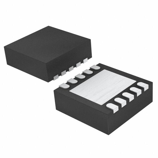
2.5-mm × 2.5-mm, 10-pin WSON package
2 Applications
•
•
•
•
•
•
Macro remote radio units (RRU)
Outdoor backhaul units
Active antenna system mMIMO (AAS)
Ultrasound scanners
Lab and field instrumentation
Sensor, imaging, and radar
The TPS7A90 output is adjustable with external
resistors from 0.8 V to 5.7 V. The TPS7A90 wide
input voltage range supports operation as low as
1.4 V and up to 6.5 V.
With 1% output voltage accuracy (over line, load, and
temperature) and soft-start capabilities to reduce inrush current, the TPS7A90 is ideal for powering
sensitive analog low-voltage devices [such as
voltage-controlled oscillators (VCOs), analog-to-digital
converters (ADCs), and digital-to-analog converters
(DACs)].
The TPS7A90 is designed to power noise-sensitive
components such as those found in high-speed
communication, video, medical, or test and
measurement applications. The very low 4.7-µVRMS
output noise and wideband PSRR (30 dB at 1 MHz)
minimizes phase noise and clock jitter. These
features maximize performance of clocking devices,
ADCs, and DACs.
Device Information(1)
PART NUMBER
TPS7A90
PACKAGE
BODY SIZE (NOM)
WSON (10)
2.50 mm × 2.50 mm
(1) For all available packages, see the orderable addendum at
the end of the datasheet.
Typical Application Circuit
2.0 V
IN
CIN
10 PF
Typical Application Diagram
TPS7A90
OUT
R1 5.9 k:
EN
FB
1.2 V
COUT
10 F
ENABLE
VIN
SS_CTRL
CNR/SS
0.1 PF
NR/SS
PG
GND
IN
CIN
CFF 10 nF
R2
VOUT
11.8 k:
RPG
20 k:
PG
Clock
PG
OUT
LMK03328
LMX2581
VDD_VCO
COUT
TPS7A90
EN
EN
GND
VDD
ADC
SCLK
ADC3xxx
ADC3xJxx
ADC3xJBxx
ADS4xxBxx
ADS5xJxx
ADS12Jxxxx
1
An IMPORTANT NOTICE at the end of this data sheet addresses availability, warranty, changes, use in safety-critical applications,
intellectual property matters and other important disclaimers. PRODUCTION DATA.
�TPS7A90
SBVS324A – JUNE 2017 – REVISED JUNE 2020
www.ti.com
Table of Contents
1
2
3
4
5
6
7
Features ..................................................................
Applications ...........................................................
Description .............................................................
Revision History.....................................................
Pin Configuration and Functions .........................
Specifications.........................................................
1
1
1
2
3
3
6.1
6.2
6.3
6.4
6.5
6.6
3
4
4
4
5
6
Absolute Maximum Ratings ......................................
ESD Ratings..............................................................
Recommended Operating Conditions.......................
Thermal Information ..................................................
Electrical Characteristics...........................................
Typical Characteristics ..............................................
Detailed Description ............................................ 12
7.1
7.2
7.3
7.4
Overview .................................................................
Functional Block Diagram .......................................
Feature Description.................................................
Device Functional Modes........................................
12
12
12
16
8
Application and Implementation ........................ 17
8.1 Application Information............................................ 17
8.2 Typical Application .................................................. 21
9 Power Supply Recommendations...................... 22
10 Layout................................................................... 22
10.1 Layout Guidelines ................................................. 22
10.2 Layout Example .................................................... 23
11 Device and Documentation Support ................. 24
11.1
11.2
11.3
11.4
11.5
11.6
11.7
Device Support ....................................................
Documentation Support ........................................
Receiving Notification of Documentation Updates
Support Resources ...............................................
Trademarks ...........................................................
Electrostatic Discharge Caution ............................
Glossary ................................................................
24
24
24
25
25
25
25
12 Mechanical, Packaging, and Orderable
Information ........................................................... 25
4 Revision History
NOTE: Page numbers for previous revisions may differ from page numbers in the current version.
Changes from Original (June 2017) to Revision A
Page
•
Changed Applications section ............................................................................................................................................... 1
•
Changed VIT(PG) parameter to VIT(PG–), added VIT(PG+) parameter row to Electrical Characteristics table ............................... 5
2
Submit Documentation Feedback
Copyright © 2017–2020, Texas Instruments Incorporated
Product Folder Links: TPS7A90
�TPS7A90
www.ti.com
SBVS324A – JUNE 2017 – REVISED JUNE 2020
5 Pin Configuration and Functions
DSK Package
2.5-mm × 2.5-mm, 10-Pin WSON
Top View
OUT
1
10
IN
OUT
2
9
IN
FB
3
8
NR/SS
GND
4
7
EN
PG
5
6
SS_CTRL
Thermal
Pad
Not to scale
Pin Functions
PIN
NAME
NO.
I/O
DESCRIPTION
EN
7
I
Enable pin. This pin turns the LDO on and off. If VEN ≥ VIH(EN), the regulator is enabled. If VEN ≤ VIL(EN),
the regulator is disabled. The EN pin must be connected to IN if the enable function is not used.
FB
3
I
Feedback pin.
This pin is the input to the control loop error amplifier and is used to set the output voltage of the device.
GND
4
—
9, 10
I
8
—
Noise reduction pin.
Connect this pin to an external capacitor to bypass the noise generated by the internal band-gap reference. The
capacitor reduces the output noise to very low levels and sets the output ramp rate to limit in-rush current.
1, 2
O
Regulated output. A 10-µF or greater capacitor must be connected from this pin to GND for stability.
PG
5
O
Open-drain, power-good indicator pin for the LDO output voltage. A 10-kΩ to 100-kΩ external pullup resistor is
required. This pin can be left floating or connected to GND if not used.
SS_CTRL
6
I
Soft-start control pin. Connect this pin either to GND or IN to change the NR/SS capacitor charging current.
If a CNR/SS capacitor is not used, SS_CTRL must be connected to GND to avoid output overshoot.
Pad
—
IN
NR/SS
OUT
Thermal pad
Device GND. Connect to the device thermal pad.
Input pin. A 10-µF or greater input capacitor is required.
Connect the thermal pad to the printed circuit board (PCB) ground plane. For an example layout, see Figure 42.
6 Specifications
6.1 Absolute Maximum Ratings
over operating junction temperature range and all voltages with respect to GND (unless otherwise noted) (1)
Voltage
Current
Temperature
(1)
MIN
MAX
IN, PG, EN
–0.3
7.0
IN, PG, EN (5% duty cycle, pulse duration ≤ 200 µs)
–0.3
7.5
OUT
–0.3
VIN + 0.3
SS_CTRL
–0.3
VIN + 0.3
NR/SS, FB
–0.3
3.6
OUT
UNIT
Internally limited
PG (sink current into the device)
V
A
5
mA
Operating junction, TJ
–55
150
°C
Storage, Tstg
–55
150
°C
Stresses beyond those listed under Absolute Maximum Ratings may cause permanent damage to the device. These are stress ratings
only, which do not imply functional operation of the device at these or any other conditions beyond those indicated under Recommended
Operating Conditions. Exposure to absolute-maximum-rated conditions for extended periods may affect device reliability.
Submit Documentation Feedback
Copyright © 2017–2020, Texas Instruments Incorporated
Product Folder Links: TPS7A90
3
�TPS7A90
SBVS324A – JUNE 2017 – REVISED JUNE 2020
www.ti.com
6.2 ESD Ratings
VALUE
V(ESD)
(1)
(2)
Electrostatic discharge
Human body model (HBM), per ANSI/ESDA/JEDEC JS-001 (1)
±2000
Charged device model (CDM), per JEDEC specification JESD22-C101 (2)
±500
UNIT
V
JEDEC document JEP155 states that 500-V HBM allows safe manufacturing with a standard ESD control process.
JEDEC document JEP157 states that 250-V CDM allows safe manufacturing with a standard ESD control process.
6.3 Recommended Operating Conditions
over operating junction temperature range (unless otherwise noted)
MIN
MAX
UNIT
VIN
Input supply voltage range
1.4
6.5
V
VOUT
Output voltage range
0.8
5.7
V
IOUT
Output current
0
0.5
CIN
Input capacitor
10
COUT
Output capacitor
10
CNR/SS
Noise-reduction capacitor
0
10
µF
CFF
Feedforward capacitor
0
100
nF
RPG
Power-good pullup resistance
10
100
kΩ
TJ
Junction temperature
–40
125
°C
A
µF
µF
6.4 Thermal Information
TPS7A90
THERMAL METRIC (1)
DSK (SON)
UNIT
10 PINS
RθJA
Junction-to-ambient thermal resistance
56.9
°C/W
RθJC(top)
Junction-to-case (top) thermal resistance
46.3
°C/W
RθJB
Junction-to-board thermal resistance
29.1
°C/W
ψJT
Junction-to-top characterization parameter
0.8
°C/W
ψJB
Junction-to-board characterization parameter
29.4
°C/W
RθJC(bot)
Junction-to-case (bottom) thermal resistance
3.2
°C/W
(1)
4
For more information about traditional and new thermal metrics, see the Semiconductor and IC Package Thermal Metrics application
report.
Submit Documentation Feedback
Copyright © 2017–2020, Texas Instruments Incorporated
Product Folder Links: TPS7A90
�TPS7A90
www.ti.com
SBVS324A – JUNE 2017 – REVISED JUNE 2020
6.5 Electrical Characteristics
over operating temperature range (TJ = –40°C to +125°C), 1.4 V ≤ VIN ≤ 6.5 V, VOUT(NOM) = 0.8 V, IOUT = 5 mA, VEN = 1.4 V,
CIN = COUT = 10 μF, CNR/SS = CFF = 0 nF, SS_CTRL = GND, and PG pin pulled up to VIN with 100 kΩ (unless otherwise
noted); typical values are at TJ = 25°C
PARAMETER
VIN
Input supply voltage range
VREF
Reference voltage
VUVLO
Input supply UVLO
VHYS(UVLO)
Input supply UVLO hysteresis
VOUT
TEST CONDITIONS
ΔVOUT(ΔVIN)
Line regulation
ΔVOUT(ΔIOUT)
Load regulation (2)
TYP
1.4
MAX
UNIT
6.5
V
0.8
VIN rising
1.31
V
1.39
V
290
Output voltage range
Output voltage accuracy (1)
MIN
1.4 V ≤ VIN ≤ 6.5 V, 5 mA ≤ IOUT ≤ 0.5 A
mV
0.8
5.7
–1.0%
1.0%
V
0.005
5 mA ≤ IOUT ≤ 0.5 A
%/V
0.02
%/A
1.4 V ≤ VIN ≤ 5.0 V, IOUT = 0.5 A, VFB = 0.8 V – 3%
100
5.0 V < VIN ≤ 5.7 V, IOUT = 0.5 A, VFB = 0.8 V – 3%
200
VDO
Dropout voltage
ILIM
Output current limit
IGND
GND pin current
ISDN
Shutdown GND pin current
PG = (open), VIN = 6.5 V, VEN = 0.4 V
IEN
EN pin current
VIN = 6.5 V, 0 V ≤ VEN ≤ 6.5 V
VIL(EN)
EN pin low-level input voltage
(device disabled)
VIH(EN)
EN pin high-level input voltage
(device enabled)
ISS_CTRL
SS_CTRL pin current
VIT(PG+)
VOUT forced at 0.9 × VOUT(NOM),
VIN = VOUT(NOM) + 300 mV
0.8
VIN = 6.5 V, IOUT = 5 mA
1.1
1.5
2.1
3.5
VIN = 1.4 V, IOUT = 0.5 A
mV
A
mA
4
15
µA
–0.2
0.2
µA
0
0.4
V
1.1
6.5
V
VIN = 6.5 V, 0 V ≤ VSS_CTRL ≤ 6.5 V
–0.2
0.2
µA
PG pin threshold rising
For PG transitioning low with rising VOUT, expressed as
a percentage of VOUT(NOM)
84%
90.9%
95%
VIT(PG–)
PG pin threshold falling
For PG transitioning low with falling VOUT, expressed as
a percentage of VOUT(NOM)
82%
88.9%
93%
VHYS(PG)
PG pin hysteresis
For PG transitioning high with rising VOUT, expressed as
a percentage of VOUT(NOM)
VOL(PG)
PG pin low-level output voltage VOUT < VIT(PG), IPG = –1 mA (current into device)
ILKG(PG)
PG pin leakage current
INR/SS
NR/SS pin charging current
IFB
FB pin leakage current
VIN = 6.5 V, VFB = 0.8 V
PSRR
Power-supply ripple rejection
f = 500 kHz, VIN = 3.8 V, VOUT(NOM) = 3.3 V,
IOUT = 250mA, CNR/SS = 10 nF, CFF = 10 nF
39
dB
Vn
Output noise voltage
BW = 10 Hz to 100 kHz, VIN = 1.8 V, VOUT(NOM) = 0.8 V,
IOUT = 0.5 A, CNR/SS = 10 nF, CFF = 10 nF
4.7
µVRMS
Noise spectral density
f = 10 kHz, VIN = 1.8 V, VOUT(NOM) = 0.8 V,
IOUT = 0.5 A, CNR/SS = 10 nF, CFF = 10 nF
13
nV/√Hz
Rdiss
Output active discharge
resistance
VEN = GND
250
Ω
Tsd
Thermal shutdown temperature
Shutdown, temperature increasing
160
Reset, temperature decreasing
140
(1)
(2)
0.1
1%
VOUT > VIT(PG), VPG = 6.5 V
0.4
V
1
µA
VNR/SS = GND, VSS_CTRL = GND
4.0
6.2
9.0
VNR/SS = GND, VSS_CTRL = VIN
65
100
150
–100
µA
100
nA
°C
When the device is connected to external feedback resistors at the FB pin, external resistor tolerances are not included.
The device is not tested under conditions where VIN > VOUT + 2.5 V and IOUT = 0.5 A because the power dissipation is higher than the
maximum rating of the package. Also, this accuracy specification does not apply on any application condition that exceeds the power
dissipation limit of the package under test.
Submit Documentation Feedback
Copyright © 2017–2020, Texas Instruments Incorporated
Product Folder Links: TPS7A90
5
�TPS7A90
SBVS324A – JUNE 2017 – REVISED JUNE 2020
www.ti.com
6.6 Typical Characteristics
at TJ = 25°C, 1.4 V ≤ VIN ≤ 6.5 V, VIN ≥ VOUT(NOM) + 0.3 V, VOUT = 0.8 V, SS_CTRL = GND, IOUT = 5 mA, VEN = 1.1 V, COUT =
10 μF, CNR/SS = CFF = 0 nF, PG pin pulled up to VOUT with 100 kΩ, and SS_CTRL = GND (unless otherwise noted)
70
Power-Supply Rejection Ratio (dB)
Power-Supply Rejection Ratio (dB)
70
60
50
40
30
20
10
0
10
VIN
1.4 V
1.5 V
1.8 V
100
2.0 V
2.5 V
3.0 V
1k
10k
100k
Frequency (Hz)
1M
60
50
40
30
10
0
10
10M
VOUT = 0.8 V, IOUT = 500 mA, COUT = 10 µF,
CNR/SS = CFF = 10 nF
Figure 1. PSRR vs Frequency and Input Voltage
40
30
VIN
3.5 V
3.6 V
3.7 V
100
3.8 V
4.0 V
4.3 V
1k
10k
100k
Frequency (Hz)
1M
40
30
20
100
5.5 V
6V
6.5 V
1k
10k
100k
Frequency (Hz)
1M
10M
VOUT = 5 V, IOUT = 500 mA, COUT = 10 µF,
CNR/SS = CFF = 10 nF
Figure 4. PSRR vs Frequency and Input Voltage
70
Power-Supply Rejection Ratio (dB)
Power-Supply Rejection Ratio (dB)
VIN
5.2 V
5.3 V
5.4 V
10
Figure 3. PSRR vs Frequency and Input Voltage
6
10M
50
0
10
10M
70
60
50
40
30
20
0
10
1M
60
VOUT = 3.3 V, IOUT = 500 mA, COUT = 10 µF,
CNR/SS = CFF = 10 nF
10
10k
100k
Frequency (Hz)
Figure 2. PSRR vs Frequency and Input Voltage
Power-Supply Rejection Ratio (dB)
Power-Supply Rejection Ratio (dB)
50
0
10
1k
70
60
10
100
2.2 V
2.5 V
3.0 V
VOUT = 1.2 V, IOUT = 500 mA, COUT = 10 µF,
CNR/SS = CFF = 10 nF
70
20
VIN
1.4 V
1.5 V
1.7 V
2.0 V
20
IOUT = 10 mA
IOUT = 50 mA
IOUT = 100 mA
100
1k
IOUT = 250 mA
IOUT = 500 mA
10k
100k
Frequency (Hz)
1M
10M
60
50
40
30
20
IOUT = 10 mA
IOUT = 50 mA
IOUT = 100 mA
10
0
10
100
1k
IOUT = 250 mA
IOUT = 500 mA
10k
100k
Frequency (Hz)
1M
10M
VOUT = 1.2 V, VIN = VEN = 1.5 V, COUT = 10 µF,
CNR/SS = CFF = 10 nF
VOUT = 3.3 V, VIN = VEN = 3.6 V, COUT = 10 µF,
CNR/SS = CFF = 10 nF
Figure 5. PSRR vs Frequency and Output Current
Figure 6. PSRR vs Frequency and Output Current
Submit Documentation Feedback
Copyright © 2017–2020, Texas Instruments Incorporated
Product Folder Links: TPS7A90
�TPS7A90
www.ti.com
SBVS324A – JUNE 2017 – REVISED JUNE 2020
Typical Characteristics (continued)
at TJ = 25°C, 1.4 V ≤ VIN ≤ 6.5 V, VIN ≥ VOUT(NOM) + 0.3 V, VOUT = 0.8 V, SS_CTRL = GND, IOUT = 5 mA, VEN = 1.1 V, COUT =
10 μF, CNR/SS = CFF = 0 nF, PG pin pulled up to VOUT with 100 kΩ, and SS_CTRL = GND (unless otherwise noted)
10
1
50
40
30
20
0.1
100
CNR = 1 uF
CNR = 10 uF
1k
10k
100k
Frequency (Hz)
1M
0.001
10
10M
VOUT = 1.2 V, VIN = VEN = 1.7 V, IOUT = 500 mA, COUT = 10 µF,
CFF = 10 nF
1k
10k
100k
Frequency (Hz)
1M
10M
Figure 8. Spectral Noise Density vs Frequency and
Output Voltage
10
10
CNR
None, 10.5 PVRMS
10 nF, 5.2 PVRMS
100 nF, 4.8 PVRMS
CFF
None, 7.7 PVRMS
10 nF, 5.0 PVRMS
100 nF, 5.2 PVRMS
1 PF, 4.7 PVRMS
10µF, 4.7 PVRMS
1
Noise (PV—Hz)
1
0.1
0.01
0.001
10
100
VIN = VOUT + 1.0 V, IOUT = 500 mA, CIN = COUT = 10 µF,
CNR/SS = CFF = 10 nF, VRMS BW = 10 Hz to 100 kHz
Figure 7. PSRR vs Frequency and CNR/SS
Noise (PV—Hz)
3.3 V, 9.2 PVRMS
5 V, 12.2 PVRMS
0.01
CNR = Open
CNR = 10 nF
CNR = 100 nF
10
0
10
0.1
0.01
100
1k
10k
100k
Frequency (Hz)
1M
0.001
10
10M
VIN = 2.2 V, VOUT = 1.2 V, IOUT = 500 mA, CIN = COUT = 10 µF,
CFF = 10 nF, VRMS BW = 10 Hz to 100 kHz
100
1k
10k
100k
Frequency (Hz)
1M
10M
VIN = 2.2 V, VOUT = 1.2 V, IOUT = 500 mA, CIN = COUT = 10 µF,
CNR/SS = 10 nF, VRMS BW = 10 Hz to 100 kHz
Figure 10. Spectral Noise Density vs Frequency and CFF
Figure 9. Spectral Noise Density vs Frequency and CNR/SS
10
1.6
COUT
10 PF, 5.2 PVRMS
22 PF, 5.2 PVRMS
100 PF, 6 PVRMS
0.1
0.01
-40qC
0qC
1.5
Temperature
25qC
85qC
125qC
1.4
Current Limit (A)
1
Noise (PV—Hz)
VOUT
0.8 V, 4.7 PVRMS
1.2 V, 5.3 PVRMS
1.8 V, 6.5 PVRMS
60
Noise (PV—Hz)
Power-Supply Rejection Ratio (dB)
70
1.3
1.2
1.1
1
0.9
0.001
10
0.8
100
1k
10k
100k
Frequency (Hz)
1M
10M
0
VIN = 2.2 V, VOUT = 1.2 V, IOUT = 500 mA, CIN = 10 µF,
CNR/SS = CFF = 10 nF, VRMS BW = 10 Hz to 100 kHz
Figure 11. Spectral Noise Density vs Frequency and COUT
100
200
300
400
500
Output Voltage (mV)
600
700
VIN = 1.4 V, VOUT = 0.8 V
Figure 12. Current Limit Foldback
Submit Documentation Feedback
Copyright © 2017–2020, Texas Instruments Incorporated
Product Folder Links: TPS7A90
800
7
�TPS7A90
SBVS324A – JUNE 2017 – REVISED JUNE 2020
www.ti.com
Typical Characteristics (continued)
at TJ = 25°C, 1.4 V ≤ VIN ≤ 6.5 V, VIN ≥ VOUT(NOM) + 0.3 V, VOUT = 0.8 V, SS_CTRL = GND, IOUT = 5 mA, VEN = 1.1 V, COUT =
10 μF, CNR/SS = CFF = 0 nF, PG pin pulled up to VOUT with 100 kΩ, and SS_CTRL = GND (unless otherwise noted)
1.4
100
80
Dropout Voltage (mV)
1.35
Current Limit (A)
-40qC
0qC
1.3
1.25
Temperature
25qC
85qC
125qC
60
40
20
1.2
-50
0
-25
0
25
50
75
Temperature (qC)
100
125
150
0
100
200
300
Output Current (mA)
VIN = 1.4 V, VOUT = 0.8 V
500
VIN = 5.5 V
Figure 13. Current Limit vs Temperature
Figure 14. Dropout Voltage vs Output Current
0.5
250
-40qC
0qC
200
Temperature
25qC
85qC
0.4
125qC
-40qC
0qC
0.3
Temperature
25qC
85qC
125qC
0.2
Accuracy (%)
Dropout Voltage (mV)
400
150
100
0.1
0
-0.1
-0.2
-0.3
50
-0.4
-0.5
0
1
1.5
2
2.5
3
3.5
4
Input Voltage (V)
4.5
5
5.5
0
6
100
200
300
Output Current (mA)
IOUT = 500 mA
500
VIN = 1.4 V
Figure 15. Dropout Voltage vs Input Voltage
Figure 16. Load Regulation
0.5
3
0.4
-40qC
0qC
Temperature
25qC
85qC
125qC
2.5
Shutdown Current (PA)
0.3
0.2
Accuracy (%)
400
0.1
0
-0.1
-0.2
-0.3
-40qC
0qC
Temperature
25qC
85qC
1
2
125qC
2
1.5
1
0.5
-0.4
-0.5
0
1
1.5
2
2.5
3
3.5
4
4.5
Input Voltage (V)
5
5.5
6
6.5
0
0.5
IOUT = 50 mA
Figure 17. Line Regulation
8
1.5
2.5 3 3.5 4 4.5
Input Voltage (V)
5
5.5
6
6.5
VEN = 0.4 V
Figure 18. Shutdown Current vs Input Voltage
Submit Documentation Feedback
Copyright © 2017–2020, Texas Instruments Incorporated
Product Folder Links: TPS7A90
�TPS7A90
www.ti.com
SBVS324A – JUNE 2017 – REVISED JUNE 2020
Typical Characteristics (continued)
at TJ = 25°C, 1.4 V ≤ VIN ≤ 6.5 V, VIN ≥ VOUT(NOM) + 0.3 V, VOUT = 0.8 V, SS_CTRL = GND, IOUT = 5 mA, VEN = 1.1 V, COUT =
10 μF, CNR/SS = CFF = 0 nF, PG pin pulled up to VOUT with 100 kΩ, and SS_CTRL = GND (unless otherwise noted)
4
3
-40qC
0qC
125qC
2.5
3
Ground Current (mA)
Ground Current (mA)
3.5
Temperature
25qC
85qC
2.5
2
1.5
1
-40qC
0qC
Temperature
25qC
85qC
1
2
125qC
2
1.5
1
0.5
0.5
0
0
0
100
200
300
Output Current (mA)
400
0
500
0.5
1.5
2.5 3 3.5 4 4.5
Input Voltage (V)
5
5.5
6
6.5
VIN = 1.4 V
Figure 20. Ground Current vs Input Voltage
Figure 19. Ground Current vs Output Current
600
-40qC
0qC
500
Temperature
25qC
85qC
PG Low Level Output Voltage (mV)
PG Low Level Output Voltage (mV)
600
125qC
400
300
200
100
0
500
Temperature
25qC
85qC
125qC
400
300
200
100
0
0
0.5
1
1.5
2
PG Current (mA)
2.5
3
0
Figure 21. PG Low Level Voltage vs PG Current
(VIN = 1.4 V)
1
1.5
2
PG Current (mA)
2.5
3
100
PG Falling
PG Rising
90
PG Pin Leakage Current (nA)
92
91
90
89
88
87
86
-50
0.5
Figure 22. PG Low Level Voltage vs PG Current
(VIN = 6.5 V)
93
Power Good Threshold (%)
-40qC
0qC
80
70
60
50
40
30
20
10
-25
0
25
50
75
Temperature (qC)
100
125
150
0
-50
-25
0
25
50
75
Temperature (qC)
100
125
150
VIN = VPG = 6.5 V
Figure 23. PG Threshold vs Temperature
Figure 24. PG Leakage Current vs Temperature
Submit Documentation Feedback
Copyright © 2017–2020, Texas Instruments Incorporated
Product Folder Links: TPS7A90
9
�TPS7A90
SBVS324A – JUNE 2017 – REVISED JUNE 2020
www.ti.com
Typical Characteristics (continued)
at TJ = 25°C, 1.4 V ≤ VIN ≤ 6.5 V, VIN ≥ VOUT(NOM) + 0.3 V, VOUT = 0.8 V, SS_CTRL = GND, IOUT = 5 mA, VEN = 1.1 V, COUT =
10 μF, CNR/SS = CFF = 0 nF, PG pin pulled up to VOUT with 100 kΩ, and SS_CTRL = GND (unless otherwise noted)
150
9
VIN
1.4 V
VIN
1.4 V
140
6.5 V
NR/SS Charging Current (PA)
NR/SS Charging Current (PA)
8.5
8
7.5
7
6.5
6
5.5
5
130
120
110
100
90
80
70
4.5
4
-50
-25
0
25
50
75
Temperature (qC)
100
125
60
-50
150
Figure 25. Soft-Start Current vs Temperature
(SS_CTRL = GND)
UVLO Falling
VIH(EN)
25
50
75
Temperature (qC)
100
125
150
UVLO Rising
1.35
Undervoltage Lockout (V)
1
Enable Threshold (V)
0
1.4
VIL(EN)
0.9
0.8
0.7
0.6
0.5
1.3
1.25
1.2
1.15
1.1
1.05
0.4
-50
-25
0
25
50
75
Temperature (qC)
100
125
1
-50
150
Figure 27. Enable Threshold vs Temperature
-25
0
25
50
75
Temperature (qC)
100
125
150
Figure 28. Input UVLO Threshold vs Temperature
50
4
4.5
Output Current
Load Transient 40
3.5
60
Output Current
Load transient 45
4
30
3.5
20
3
30
3
10
2.5
15
2.5
0
2
-10
1.5
-20
1
-30
0.5
-40
0
0
-50
50 100 150 200 250 300 350 400 450 500 550 600
Time (Ps)
Figu
VIN = 1.4 V, IOUT = 50 mA to 500 mA to 50 mA at 1 A/µs,
COUT = 10 µF, VPG = VOUT
Figure 29. Load Transient Response (VOUT = 0.8 V)
Output Current (A)
5
AC-Coupled Output Voltage (mV)
Output Current (A)
-25
Figure 26. Soft-Start Current vs Temperature
(SS_CTRL = VIN)
1.1
10
6.5 V
2
0
1.5
-15
1
-30
0.5
-45
0
0
60
120
180
240 300 360
Time (Ps)
420
480
540
-60
600
Figu
VIN = 5.5 V, IOUT = 50 mA to 500 mA to 50 mA at 1 A/µs,
COUT = 10 µF, VPG = VOUT
Figure 30. Load Transient Response (VOUT = 5.0 V)
Submit Documentation Feedback
Copyright © 2017–2020, Texas Instruments Incorporated
Product Folder Links: TPS7A90
�TPS7A90
www.ti.com
SBVS324A – JUNE 2017 – REVISED JUNE 2020
Typical Characteristics (continued)
at TJ = 25°C, 1.4 V ≤ VIN ≤ 6.5 V, VIN ≥ VOUT(NOM) + 0.3 V, VOUT = 0.8 V, SS_CTRL = GND, IOUT = 5 mA, VEN = 1.1 V, COUT =
10 μF, CNR/SS = CFF = 0 nF, PG pin pulled up to VOUT with 100 kΩ, and SS_CTRL = GND (unless otherwise noted)
VEN
1 V/div
VIN
2 V/div
VOUT
200 mV/div
VOUT
20 mV/div
VPG
200mV/div
VPG
1 V/div
Time (200 Ps/div)
Time (50 Ps/div)
VIN = 1.4 V to 6.5 V to 1.4 V at 2 V/µs, VOUT = 0.8 V,
IOUT = 500 mA, CNR/SS = CFF = 10 nF, VPG = VOUT
VIN = 1.4 V, VPG = VOUT
Figure 31. Line Transient
Figure 32. Start-Up (SS_CTRL = GND, CNR/SS = 0 nF)
VEN
1 V/div
VEN
1 V/div
VOUT
200 mV/div
VOUT
200 mV/div
VPG
200 mV/div
VPG
200 mV/div
Time (50 Ps/div)
Time (500 Ps/div)
VIN = 1.4 V, VPG = VOUT
VIN = 1.4 V, VPG = VOUT
Figure 33. Start-Up (SS_CTRL = GND, CNR/SS = 10 nF)
VEN
1 V/div
Figure 34. Start-Up (SS_CTRL = VIN, CNR/SS = 10 nF)
VOUT
200 mV/div
VPG
200 mV/div
Time (2 ms/div)
VIN = 1.4 V, VPG = VOUT
Figure 35. Start-Up (SS_CTRL = VIN, CNR/SS = 1 µF)
Submit Documentation Feedback
Copyright © 2017–2020, Texas Instruments Incorporated
Product Folder Links: TPS7A90
11
�TPS7A90
SBVS324A – JUNE 2017 – REVISED JUNE 2020
www.ti.com
7 Detailed Description
7.1 Overview
The TPS7A90 is a low-noise, high PSRR, low dropout (LDO) regulator capable of sourcing a 500-mA load with
only 200 mV of maximum dropout. The TPS7A90 can operate down to a 1.4-V input voltage and a 0.8-V output
voltage. This combination of low-noise, high PSRR, and low dropout voltage makes the device an ideal LDO to
power a multitude of loads from noise-sensitive communication components in high-speed communications
applications to high-end microprocessors or field-programmable gate arrays (FPGAs).
As shown in the Functional Block Diagram section, the TPS7A90 linear regulator features a low-noise, 0.8-V
internal reference that can be filtered externally to obtain even lower output noise. The internal protection circuitry
(such as the undervoltage lockout) prevents the device from turning on before the input is high enough to ensure
accurate regulation. Foldback current limiting is also included, allowing the output to source the rated output
current when the output voltage is in regulation but reduces the allowable output current during short-circuit
conditions. The internal power-good detection circuit allows down-stream supplies to be sequenced and alerts if
the output voltage is below a regulation threshold.
7.2 Functional Block Diagram
PSRR
Boost
IN
Current
Limit
OUT
Charge
Pump
0.8-V
VREF
SS_CTRL
Soft-Start
Control
Active
Discharge
RNR/SS = 280 k:
+
Error
Amp
±
INR/SS
NR/SS
200 pF
FB
UVLO
Circuits
Internal
Controller
±
0.889 x VREF
PG
+
Thermal
Shutdown
EN
GND
7.3 Feature Description
7.3.1 Output Enable
The enable pin (EN) for the TPS7A90 is active high. The output voltage is enabled when the enable pin voltage
is greater than VIH(EN) and disabled with the enable pin voltage is less than VIL(EN). If independent control of the
output voltage is not needed, then connect the enable pin to the input.
The TPS7A90 has an internal pulldown MOSFET that connects a discharge resistor from VOUT to ground when
the device is disabled to actively discharge the output voltage.
7.3.2 Dropout Voltage (VDO)
Dropout voltage (VDO) is defined as the VIN – VOUT voltage at the rated current (IRATED) of 500 mA, where the
pass-FET is fully on and in the ohmic region of operation. VDO indirectly specifies a minimum input voltage above
the nominal programmed output voltage at which the output voltage is expected to remain in regulation. If the
input falls below the nominal output regulation, then the output follows the input.
12
Submit Documentation Feedback
Copyright © 2017–2020, Texas Instruments Incorporated
Product Folder Links: TPS7A90
�TPS7A90
www.ti.com
SBVS324A – JUNE 2017 – REVISED JUNE 2020
Feature Description (continued)
Dropout voltage is determined by the RDS(ON) of the pass-FET. Therefore, if the LDO operates below the rated
current, then the VDO for that current scales accordingly. Use Equation 1 to calculate the RDS(ON) for the
TPS7A90:
VDO
RDS(ON) =
IRATED
(1)
7.3.3 Output Voltage Accuracy
Output voltage accuracy specifies minimum and maximum output voltage error, relative to the expected nominal
output voltage stated as a percent. The TPS7A90 features an output voltage accuracy of 1% that includes the
errors introduced by the internal reference, load regulation, and line regulation variance across the full range of
rated load and line operating conditions over temperature, as specified by the Electrical Characteristics table.
Output voltage accuracy also accounts for all variations between manufacturing lots.
7.3.4 High Power-Supply Rejection Ratio (PSRR)
PSRR is a measure of how well the LDO control loop rejects noise from the input source to make the dc output
voltage as noise-free as possible across the frequency spectrum (usually measured from 10 Hz to 10 MHz).
Even though PSRR is a loss in noise signal amplitude, the PSRR curves in the Typical Characteristics section
are illustrated as positive values in decibels (dB) for convenience. Equation 2 gives the PSRR calculation as a
function of frequency where input noise voltage [VIN(f)] and output noise voltage [VOUT(f)] are the amplitudes of
the respective sinusoidal signals.
§ V (f ) ·
PSRR (dB) 20 Log10 ¨ IN
¸
© VOUT (f ) ¹
(2)
Noise that couples from the input to the internal reference voltage is a primary contributor to reduced PSRR
performance. Using a noise-reduction capacitor is recommended to filter unwanted noise from the input voltage,
which creates a low-pass filter with an internal resistor to improve PSRR performance at lower frequencies.
LDOs are often employed not only as a step-down regulators, but also to provide exceptionally clean power rails
for noise-sensitive components. This usage is especially true for the TPS7A90, which features an innovative
circuit to boost the PSRR between 200 kHz and 1 MHz. This boost circuit helps further filter switching noise from
switching-regulators that operate in this region; see Figure 1. To achieve the maximum benefit of this PSRR
boost circuit, using a capacitor with a minimum impedance in the 100-kHz to 1-MHz band is recommended.
7.3.5 Low Output Noise
LDO noise is defined as the internally-generated intrinsic noise created by the semiconductor circuits. The
TPS7A90 is designed for system applications where minimizing noise on the power-supply rail is critical to
system performance. This scenario is the case for phase-locked loop (PLL)-based clocking circuits where
minimum phase noise is all important, or in test and measurement systems where even small power-supply
noise fluctuations can distort instantaneous measurement accuracy.
The TPS7A90 includes a low-noise reference ensuring minimal output noise in normal operation. Further
improvements can be made by adding a noise-reduction capacitor (CNR/SS), a feedforward capacitor (CFF), or a
combination of the two. See the Noise-Reduction and Soft-Start Capacitor (CNR/SS) and Feed-Forward Capacitor
(CFF) sections for additional design information.
For more information on noise and noise measurement, see the How to Measure LDO Noise white paper.
7.3.6 Output Soft-Start Control
Soft-start refers to the ramp-up characteristic of the output voltage during LDO turn-on after the EN and UVLO
thresholds are exceeded. The noise-reduction capacitor (CNR/SS) serves a dual purpose of both governing output
noise reduction and programming the soft-start ramp during turn-on. Larger values for the noise-reduction
capacitors decrease the noise but also result in a slower output turn-on ramp rate.
Submit Documentation Feedback
Copyright © 2017–2020, Texas Instruments Incorporated
Product Folder Links: TPS7A90
13
�TPS7A90
SBVS324A – JUNE 2017 – REVISED JUNE 2020
www.ti.com
Feature Description (continued)
The TPS7A90 features an SS_CTRL pin. When the SS_CTRL pin is grounded, the charging current for the
NR/SS pin is 6.2 µA (typ); when this pin is connected to IN, the charging current for the NR/SS pin is increased
to 100 µA (typ). The higher current allows the use of a much larger noise-reduction capacitor and maintains a
reasonable startup time. Figure 36 shows a simplified block diagram of the soft-start circuit. The switch SW is
opened to turn off the INR/SS current source after VFB reaches approximately 97% of VREF. The final 3% of VNR/SS
is charged through the noise-reduction resistor (RNR), which creates an RC delay. RNR is approximately 280 kΩ
and applications that require the highest accuracy when using a large value CNR/SS must take this RC delay into
account.
If a noise-reduction capacitor is not used on the NR/SS pin, tying the SS_CTRL pin to the IN pin can result in
output voltage overshoot of approximately 10%. This overshoot is minimized by either connecting the SS_CTRL
pin to GND or using a capacitor on the NR/SS pin.
SW
INR/SS
RNR
NR/SS Control
VREF
+
CNR/SS
VFB
±
GND
Figure 36. Simplified Soft-Start Circuit
7.3.7 Power-Good Function
The power-good circuit monitors the voltage at the feedback pin to indicate the status of the output voltage.
When the feedback pin voltage falls below the PG threshold voltage (VIT(PG)), the PG pin open-drain output
engages and pulls the PG pin close to GND. When the feedback voltage exceeds the VIT(PG) threshold by an
amount greater than VHYS(PG), the PG pin becomes high impedance. By connecting a pullup resistor to an
external supply, any downstream device can receive power-good as a logic signal that can be used for
sequencing. Make sure that the external pullup supply voltage results in a valid logic signal for the receiving
device or devices. Using a pullup resistor from 10 kΩ to 100 kΩ is recommended. Using an external reset device
such as the TPS3890 is also recommended in applications where high accuracy is needed or in applications
where microprocessor induced resets are needed.
When using a feed-forward capacitor (CFF), the time constant for the LDO startup is increased whereas the
power-good output time constant stays the same, possibly resulting in an invalid status of the power-good output.
To avoid this issue and to receive a valid PG output, make sure that the time constant of both the LDO startup
and the power-good output are matching, which can be done by adding a capacitor in parallel with the powergood pullup resistor. For more information, see the application report Pros and Cons of Using a Feedforward
Capacitor with a Low-Dropout Regulator.
The state of PG is only valid when the device is operating above the minimum input voltage of the device and
power-good is asserted regardless of the output voltage state when the input voltage falls below the UVLO
threshold minus the UVLO hysteresis. Figure 37 illustrates a simplified block diagram of the power-good circuit.
When the input voltage falls below approximately 0.8 V, there is not enough gate drive voltage to keep the opendrain, power-good device turned on and the power-good output is pulled high. Connecting the power-good pullup
resistor to the output voltage can help minimize this effect.
14
Submit Documentation Feedback
Copyright © 2017–2020, Texas Instruments Incorporated
Product Folder Links: TPS7A90
�TPS7A90
www.ti.com
SBVS324A – JUNE 2017 – REVISED JUNE 2020
Feature Description (continued)
VPG
VREF
VIN
VFB
±
+
GND
EN UVLO
GND
GND
Figure 37. Simplified PG Circuit
7.3.8 Internal Protection Circuitry
7.3.8.1 Undervoltage Lockout (UVLO)
The TPS7A90 has an independent undervoltage lockout (UVLO) circuit that monitors the input voltage, allowing
a controlled and consistent turn on and off of the output voltage. To prevent the device from turning off if the
input drops during turn on, the UVLO has approximately 290 mV of hysteresis.
The UVLO circuit responds quickly to glitches on VIN and disables the output of the device if this rail starts to
collapse too quickly. Use an input capacitor that is large enough to slow input transients to less then two volts
per microsecond.
7.3.8.2 Internal Current Limit (ICL)
The internal current-limit circuit is used to protect the LDO against transient high-load current faults or shorting
events. The LDO is not designed to operate in current limit under steady-state conditions. During an overcurrent
event where the output voltage is pulled 10% below the regulated output voltage, the LDO sources a constant
current as specified in the Electrical Characteristics table. When the output voltage falls, the amount of output
current is reduced to better protect the device. During a hard short-circuit event, the current is reduced to
approximately 1.45 A. See Figure 12 in the Typical Characteristics section for more information about the
current-limit foldback behavior. However, when a current-limit event occurs, the LDO begins to heat up because
of the increase in power dissipation. The increase in heat can trigger the integrated thermal shutdown protection
circuit.
7.3.8.3 Thermal Protection
The TPS7A90 contains a thermal shutdown protection circuit to turn off the output current when excessive heat is
dissipated in the LDO. Thermal shutdown occurs when the thermal junction temperature (TJ) of the pass-FET
exceeds 160°C (typical). Thermal shutdown hysteresis assures that the LDO again resets (turns on) when the
temperature falls to 140°C (typical). The thermal time-constant of the semiconductor die is fairly short, and thus
the output turns on and off at a high rate when thermal shutdown is reached until power dissipation is reduced.
The internal protection circuitry of the TPS7A90 is designed to protect against thermal overload conditions. The
circuitry is not intended to replace proper heat sinking. Continuously running the TPS7A90 into thermal shutdown
degrades device reliability.
For reliable operation, limit junction temperature to a maximum of 125°C. To estimate the thermal margin in a
given layout, increase the ambient temperature until the thermal protection shutdown is triggered using worstcase load and highest input voltage conditions. For good reliability, thermal shutdown must occur at least 35°C
above the maximum expected ambient temperature condition for the application. This configuration produces a
worst-case junction temperature of 125°C at the highest expected ambient temperature and worst-case load.
Submit Documentation Feedback
Copyright © 2017–2020, Texas Instruments Incorporated
Product Folder Links: TPS7A90
15
�TPS7A90
SBVS324A – JUNE 2017 – REVISED JUNE 2020
www.ti.com
7.4 Device Functional Modes
Table 1 provides a quick comparison between the normal, dropout, and disabled modes of operation.
Table 1. Device Functional Modes Comparison
PARAMETER
OPERATING MODE
(1)
(2)
VIN
EN
IOUT
TJ
Normal (1)
VIN > VOUT(nom) + VDO
VEN > VIH(EN)
IOUT < ICL
TJ < Tsd
Dropout (1)
VIN < VOUT(nom) + VDO
VEN > VIH(EN)
IOUT < ICL
TJ < Tsd
Disabled (2)
VIN < VUVLO
VEN < VIL(EN)
—
TJ > Tsd
All table conditions must be met.
The device is disabled when any condition is met.
7.4.1 Normal Operation
The device regulates to the nominal output voltage when all of the following conditions are met:
• The input voltage is greater than the nominal output voltage plus the dropout voltage (VOUT(nom) + VDO)
• The enable voltage has previously exceeded the enable rising threshold voltage and has not yet decreased
below the enable falling threshold
• The output current is less than the current limit (IOUT < ICL)
• The device junction temperature is less than the thermal shutdown temperature (TJ < Tsd)
7.4.2 Dropout Operation
If the input voltage is lower than the nominal output voltage plus the specified dropout voltage, but all other
conditions are met for normal operation, the device operates in dropout. In this mode, the output voltage tracks
the input voltage. During this mode, the transient performance of the device becomes significantly degraded
because the pass device is in a triode state and no longer controls the current through the LDO. Line or load
transients in dropout can result in large output-voltage deviations.
When the device is in a steady dropout state (defined as when the device is in dropout, VIN < VOUT(NOM) + VDO,
right after being in a normal regulation state, but not during startup), the pass-FET is driven as hard as possible.
When the input voltage returns to VIN ≥ VOUT(NOM) + VDO, VOUT can overshoot for a short period of time if the input
voltage slew rate is greater than 0.1 V/µs.
7.4.3 Disabled
The output of the TPS7A90 can be shutdown by forcing the enable pin below 0.4 V. When disabled, the pass
device is turned off, internal circuits are shutdown, and the output voltage is actively discharged to ground by an
internal resistor from the output to ground.
16
Submit Documentation Feedback
Copyright © 2017–2020, Texas Instruments Incorporated
Product Folder Links: TPS7A90
�TPS7A90
www.ti.com
SBVS324A – JUNE 2017 – REVISED JUNE 2020
8 Application and Implementation
NOTE
Information in the following applications sections is not part of the TI component
specification, and TI does not warrant its accuracy or completeness. TI’s customers are
responsible for determining suitability of components for their purposes. Customers should
validate and test their design implementation to confirm system functionality.
8.1 Application Information
The TPS7A90 is a linear voltage regulator operating from 1.4 V to 6.5 V on the input, and regulates voltages
between 0.8 V to 5.0 V within 1% accuracy and a 500-mA maximum output current. Efficiency is defined by the
ratio of output voltage to input voltage because the TPS7A90 is a linear voltage regulator. To achieve high
efficiency, the dropout voltage (VIN – VOUT) must be as small as possible, thus requiring a very low dropout LDO.
Successfully implementing an LDO in an application depends on the application requirements. This section
discusses key device features and how to best implement them to achieve a reliable design.
8.1.1 Adjustable Output
As Figure 38 shows, the output voltage of the TPS7A9001 can be adjusted from 0.8 V to 5.2 V by using a
resistor divider network.
VIN
IN
CIN
VOUT
OUT
R1
EN
FB
COUT
SS_CTRL
NR/SS
CNR/SS
PG
R2
GND
Figure 38. Adjustable Operation
Use Equation 3 to calculate R1 and R2 for any output voltage range. This resistive network must provide a
current greater than or equal to 5 µA for optimum noise performance.
§V
R 1 = R 2 ¨ OUT
© VREF
·
1¸ ,
¹
where
VREF(max)
R2
! 5 PA
(3)
If greater voltage accuracy is required, take into account the output voltage offset contribution resulting from the
feedback pin current (IFB) and use 0.1%-tolerance resistors.
Submit Documentation Feedback
Copyright © 2017–2020, Texas Instruments Incorporated
Product Folder Links: TPS7A90
17
�TPS7A90
SBVS324A – JUNE 2017 – REVISED JUNE 2020
www.ti.com
Application Information (continued)
Table 2 lists the resistor combination required to achieve a few of the most common rails using commerciallyavailable, 0.1%-tolerance resistors to maximize nominal voltage accuracy and also abiding to the formula given
in Equation 3.
Table 2. Recommended Feedback-Resistor Values
(1)
FEEDBACK RESISTOR VALUES
(1)
VOUT(TARGET)
(V)
R1 (kΩ)
R2 (kΩ)
CALCULATED OUTPUT
VOLTAGE (V)
0.8
Short
Open
0.800
1.00
2.55
10.2
1.000
1.20
5.9
11.8
1.200
1.50
9.31
10.7
1.496
1.80
1.87
1.5
1.797
1.90
15.8
11.5
1.899
2.50
2.43
1.15
2.490
3.00
3.16
1.15
2.998
3.30
3.57
1.15
3.283
5.00
10.5
2
5.00
R1 is connected from OUT to FB; R2 is connected from FB to GND; see Figure 38.
8.1.2 Start-Up
8.1.2.1 Enable (EN) and Undervoltage Lockout (UVLO)
The TPS7A90 only turns on when EN and UVLO are above the respective voltage thresholds. The TPS7A90 has
an independent UVLO circuit that monitors the input voltage to allow a controlled and consistent turn on and off.
The UVLO has approximately 290 mV of hysteresis to prevent the device from turning off if the input drops
during turn on. The EN signal allows independent logic-level turn-on and shutdown of the LDO when the input
voltage is present. Connecting EN directly to IN is recommended if independent turn-on is not needed.
The TPS7A90 has an internal pulldown MOSFET that connects a discharge resistor from VOUT to ground when
the device is disabled to actively discharge the output voltage.
8.1.2.2 Noise-Reduction and Soft-Start Capacitor (CNR/SS)
The CNR/SS capacitor serves a dual purpose of both reducing output noise and setting the soft-start ramp during
turn-on.
8.1.2.2.1 Noise Reduction
For low-noise applications, the CNR/SS capacitor forms an RC filter for filtering output noise that is otherwise
amplified by the control loop. For low-noise applications, a CNR/SS of between 10 nF to 10 µF is recommended.
Larger values for CNR/SS can be used; however, above 1 µF there is little benefit in lowering the output voltage
noise for frequencies above 10 Hz.
18
Submit Documentation Feedback
Copyright © 2017–2020, Texas Instruments Incorporated
Product Folder Links: TPS7A90
�TPS7A90
www.ti.com
SBVS324A – JUNE 2017 – REVISED JUNE 2020
8.1.2.2.2 Soft-Start and In-Rush Current
Soft-start refers to the gradual ramp-up characteristic of the output voltage after the EN and UVLO thresholds are
exceeded. Reducing how quickly the output voltage increases during startup also reduces the amount of current
needed to charge the output capacitor, referred to as in-rush current. In-rush current is defined as the current
going into the LDO during start-up. In-rush current consists of the load current, the current used to charge the
output capacitor, and the ground pin current (that contributes very little to in-rush current). This current is difficult
to measure because the input capacitor must be removed, which is not recommended. However, Equation 4 can
be used to estimate in-rush current:
u dVOUT (t) · § VOUT (t) ·
§C
IOUT (t) ¨ OUT
¸
¸ ¨
dt
©
¹ © RLOAD ¹
where:
•
•
•
VOUT(t) is the instantaneous output voltage of the turn-on ramp
dVOUT(t) / dt is the slope of the VOUT ramp
RLOAD is the resistive load impedance
(4)
The TPS7A90 features a monotonic, voltage-controlled soft-start that is set with an external capacitor (CNR/SS).
This soft-start helps reduce in-rush current, minimizing load transients to the input power bus that can cause
potential start-up initialization problems when powering FPGAs, digital signal processors (DSPs), or other high
current loads.
To achieve a monotonic start-up, the TPS7A90 error amplifier tracks the voltage ramp of the external soft-start
capacitor until the voltage exceeds approximately 97% of the internal reference. The final 3% of VNR/SS is
charged through the noise-reduction resistor (RNR), creating an RC delay. RNR is approximately 280 kΩ and
applications that require the highest accuracy when using a large value CNR/SS must take this RC delay into
account.
The soft-start ramp time depends on the soft-start charging current (INR/SS), the soft-start capacitance (CNR/SS),
and the internal reference (VREF). Use Equation 5 to calculate the approximate soft-start ramp time (tSS):
tSS = (VREF × CNR/SS) / INR/SS
(5)
The value for INR/SS is determined by the state of the SS_CTRL pin. When the SS_CTRL pin is connected to
GND, the typical value for the INR/SS current is 6.2 µA. Connecting the SS_CTRL pin to IN increases the typical
soft-start charging current to 100 µA. The larger charging current for INR/SS is useful if shorter start-up times are
needed (such as when using a large noise-reduction capacitor).
8.1.3 Capacitor Recommendation
The TPS7A90 is designed to be stable using low equivalent series resistance (ESR) ceramic capacitors at the
input, output, and noise-reduction pin. Multilayer ceramic capacitors are the industry standard for these types of
applications and are recommended, but must be used with good understanding of their limitations. Ceramic
capacitors that employ X7R-, X5R-, and COG-rated dielectric materials provide relatively good capacitive stability
across temperature, whereas the use of Y5V-rated capacitors is discouraged precisely because the capacitance
varies so widely. In all cases, ceramic capacitors vary a great deal with operating voltage and temperature and
the design engineer must be aware of these characteristics. As a rule of thumb, ceramic capacitors are
recommended to be derated by 50%. The input and output capacitors recommended herein account for a
capacitance derating of 50%.
Submit Documentation Feedback
Copyright © 2017–2020, Texas Instruments Incorporated
Product Folder Links: TPS7A90
19
�TPS7A90
SBVS324A – JUNE 2017 – REVISED JUNE 2020
www.ti.com
8.1.3.1 Input and Output Capacitor Requirements (CIN and COUT)
The TPS7A90 is designed and characterized for operation with ceramic capacitors of 10 µF or greater at the
input and output. Locate the input and output capacitors as near as practical to the input and output pins to
minimize the trace inductance from the capacitor to the device.
Attention must be given to the input capacitance to minimize transient input droop during startup and load current
steps. Simply using very large ceramic input capacitances can cause unwanted ringing at the output if the input
capacitor (in combination with the wire-lead inductance) creates a high-Q peaking effect during transients, which
is why short, well-designed interconnect traces to the upstream supply are needed to minimize ringing. Damping
of unwanted ringing can be accomplished by using a tantalum capacitor, with a few hundred milliohms of ESR, in
parallel with the ceramic input capacitor. The UVLO circuit responds quickly to glitches on VIN and disables the
output of the device if this rail starts to collapse too quickly. Use an input capacitor that is large enough to slow
input transients to less then two volts per microsecond.
8.1.3.1.1 Load-Step Transient Response
The load-step transient response is the output voltage response by the LDO to a step change in load current.
The depth of charge depletion immediately after the load step is directly proportional to the amount of output
capacitance. However, although larger output capacitances decrease any voltage dip or peak occurring during a
load step, the control-loop bandwidth is also decreased, thereby slowing the response time.
The LDO cannot sink charge, therefore when the output load is removed or greatly reduced, the control loop
must turn off the pass-FET and wait for any excess charge to deplete.
8.1.3.2 Feed-Forward Capacitor (CFF)
Although a feed-forward capacitor (CFF), from the FB pin to the OUT pin is not required to achieve stability, a
10-nF, feed-forward capacitor improves the noise and PSRR performance. A higher capacitance CFF can be
used; however, the startup time is longer and the power-good signal can incorrectly indicate that the output
voltage has settled. For a detailed description, see the application report Pros and Cons of Using a Feedforward
Capacitor with a Low-Dropout Regulator.
8.1.4 Power Dissipation (PD)
Circuit reliability demands that proper consideration be given to device power dissipation, location of the circuit
on the printed circuit board (PCB), and correct sizing of the thermal plane. The PCB area around the regulator
must be as free as possible of other heat-generating devices that cause added thermal stresses.
To a first-order approximation, power dissipation in the regulator depends on the input-to-output voltage
difference and load conditions. Equation 6 calculates PD:
PD = (VIN – VOUT) × IOUT
(6)
Power dissipation can be minimized, and thus greater efficiency achieved, by proper selection of the system
voltage rails. For the lowest power dissipation use the minimum input voltage necessary for proper output
regulation.
The primary heat conduction path for the DSK package is through the thermal pad to the PCB. Solder the
thermal pad to a copper pad area under the device. This pad area should contain an array of plated vias that
conduct heat to additional copper planes for increased heat dissipation.
The maximum power dissipation determines the maximum allowable ambient temperature (TA) for the device.
According to Equation 7, power dissipation and junction temperature are most often related by the junction-toambient thermal resistance (θJA) of the combined PCB and device package and the temperature of the ambient
air (TA).
TJ = TA + (qJA ´ PD)
(7)
Unfortunately, the thermal resistance (θJA) is highly dependent on the heat-spreading capability built into the
particular PCB design, and therefore varies according to the total copper area, copper weight, and location of the
planes. The θJA recorded in the Thermal Information table is determined by the JEDEC standard, PCB, and
copper-spreading area and is only used as a relative measure of package thermal performance.
20
Submit Documentation Feedback
Copyright © 2017–2020, Texas Instruments Incorporated
Product Folder Links: TPS7A90
�TPS7A90
www.ti.com
SBVS324A – JUNE 2017 – REVISED JUNE 2020
8.1.5 Estimating Junction Temperature
The JEDEC standard recommends the use of psi (Ψ) thermal metrics to estimate the junction temperatures of
the LDO when in-circuit on a typical PCB board application. These metrics are not strictly speaking thermal
resistances, but rather offer practical and relative means of estimating junction temperatures. These psi metrics
are determined to be significantly independent of the copper-spreading area. The key thermal metrics (ΨJT and
ΨJB) are used in accordance with Equation 8 and are given in the Thermal Information table.
YJT: TJ = TT + YJT ´ PD
YJB: TJ = TB + YJB ´ PD
where:
•
•
•
PD is the power dissipated as explained in Equation 6
TT is the temperature at the center-top of the device package
TB is the PCB surface temperature measured 1 mm from the device package and centered on the package
edge
(8)
For a more detailed discussion on thermal metrics and how to use them, see the application report
Semiconductor and IC Package Thermal Metrics.
8.2 Typical Application
This section discusses the implementation of the TPS7A90 to regulate from a 2-V input voltage to a 1.2-V output
voltage for noise-sensitive loads. Figure 39 shows the schematic for this application circuit.
2.0 V
IN
CIN
10 PF
TPS7A90
OUT
EN
FB
SS_CTRL
CNR/SS
0.1 PF
1.2 V
COUT
10 F
R1 5.9 k:
NR/SS
PG
CFF 10 nF
R2
VOUT
11.8 k:
RPG
20 k:
PG
GND
Figure 39. Application Example
8.2.1 Design Requirements
For the design example shown in Figure 39, use the parameters listed in Table 3 as the input parameters.
Table 3. Design Parameters
PARAMETER
APPLICATION REQUIREMENTS
DESIGN RESULTS
2 V, ±3%, provided by the dc-dc converter
switching at 750 kHz
1.4 V to 6.5 V
85°C
108°C junction temperature
Output voltages (VOUT)
1.2 V, ±1%
1.2 V, ±1%
Output currents (IOUT)
500 mA (max), 10 mA (min)
500 mA (max), 5 mA (min)
< 6 µVRMS, bandwidth = 10 Hz to 100 kHz
5.2 µVRMS, bandwidth = 10 Hz to 100 kHz
PSRR at 500 kHz
> 40 dB
47 dB
Startup time
< 2 ms
80 µs (typ) 148 µs (max)
Input voltages (VIN)
Maximum ambient operating
temperature
RMS noise
8.2.2 Detailed Design Procedure
The output voltage can be set to 1.2 V by selecting the correct values for R1 and R2; see Equation 3.
Input and output capacitors are selected in accordance with the Capacitor Recommendation section. Ceramic
capacitances of 10 µF for both input and output are selected to help balance the charge needed during startup
when charging the output capacitor, thus reducing the input voltage drop.
Submit Documentation Feedback
Copyright © 2017–2020, Texas Instruments Incorporated
Product Folder Links: TPS7A90
21
�TPS7A90
SBVS324A – JUNE 2017 – REVISED JUNE 2020
www.ti.com
To satisfy the required startup time (tSS) and still maintain low-noise performance, a 0.01-µF CNR/SS is selected
for with SS_CTRL connected to VIN. Equation 9 calculates this value. Using INR/SS(MAX) and the smallest CNR/SS
capacitance resulting from manufacturing variance (often ±20%) provides the fastest startup time, whereas using
INR/SS(MIN) and the largest CNR/SS capacitance resulting from manufacturing variance provides the slowest startup
time.
tSS = (VREF × CNR/SS) / INR/SS
(9)
With a 500-mA maximum load, the internal power dissipation is 800 mW, corresponding to a 23°C junction
temperature rise. With an 85°C maximum ambient temperature, the junction temperature is at 108°C. To
minimize noise, a feed-forward capacitance (CFF) of 10 nF is selected.
See the Layout section for an example of how to layout the TPS7A90 to achieve best PSRR and noise.
8.2.3 Application Curves
10
5.2 PVRMS
CNR = 10 nF, CFF = 10 nF
60
1
50
Noise (PV—Hz)
Power-Supply Rejection Ratio (dB)
70
40
30
20
10
0.1
0.01
VIN
2.0 V
0
10
100
1k
10k
100k
Frequency (Hz)
1M
10M
0.001
10
Figure 40. PSRR vs Frequency
100
1k
10k
100k
Frequency (Hz)
1M
10M
Figure 41. Output Noise vs Frequency
9 Power Supply Recommendations
The input of the TPS7A90 is designed to operate from an input voltage range between 1.4 V and 6.5 V and with
an input capacitor of 10 µF. The input voltage range must provide adequate headroom in order for the device to
have a regulated output. This input supply must be well regulated. If the input supply is noisy, additional input
capacitors can be used to improve the output noise performance.
10 Layout
10.1 Layout Guidelines
General guidelines for linear regulator designs are to place all circuit components on the same side of the circuit
board and as near as practical to the respective LDO pin connections. Place ground return connections to the
input and output capacitors, and to the LDO ground pin as close to each other as possible, connected by a wide,
component-side, copper surface. The use of vias and long traces to create LDO circuit connections is strongly
discouraged and negatively affects system performance.
10.1.1 Board Layout
To maximize the ac performance of the TPS7A90, following the layout example shown in Figure 42 is
recommended. This layout isolates the analog ground (AGND) from the noisy power ground. Components that
must be connected to the quiet analog ground are the noise-reduction capacitor (CNR/SS) and the lower feedback
resistor (R2). These components must have a separate connection back to the thermal pad of the device for
optimal output noise performance. Connect the GND pin directly to the thermal pad and not to any external
plane.
22
Submit Documentation Feedback
Copyright © 2017–2020, Texas Instruments Incorporated
Product Folder Links: TPS7A90
�TPS7A90
www.ti.com
SBVS324A – JUNE 2017 – REVISED JUNE 2020
Layout Guidelines (continued)
To maximize the output voltage accuracy, the connection from the output voltage back to top output divider
resistors (R1) must be made as close as possible to the load. This method of connecting the feedback trace
eliminates the voltage drop from the device output to the load.
To improve thermal performance, use an array of thermal vias to connect the thermal pad to the ground planes.
Larger ground planes improve the thermal performance of the device and lowering the operating temperature of
the device.
10.2 Layout Example
Power Ground
Plane
COUT
CIN
OUT
1
10
IN
VOUT
VIN
OUT
2
9
IN
FB
3
8
NR/SS
GND
4
7
EN
PG
5
6
SS_CTRL
CFF
R1
CNR/SS
R2
To VIN
To PG
Pullup Supply
Ground Plane for
Thermal Relief and
Signal Ground
PG Output
Denotes vias used for application purposes
Figure 42. TPS7A90 Example Layout
Submit Documentation Feedback
Copyright © 2017–2020, Texas Instruments Incorporated
Product Folder Links: TPS7A90
23
�TPS7A90
SBVS324A – JUNE 2017 – REVISED JUNE 2020
www.ti.com
11 Device and Documentation Support
11.1 Device Support
11.1.1 Development Support
11.1.1.1 Evaluation Modules
An evaluation module (EVM) is available to assist in the initial circuit performance evaluation using the TPS7A90.
Table 4 shows the summary information for this fixture.
Table 4. Design Kits and Evaluation Modules (1)
(1)
NAME
PART NUMBER
TPS7A90EVM-831 Evaluation Module User's Guide
TPS7A90EVM-831
For the most current package and ordering information see the Package Option Addendum at the end of this document, or see the
device product folder at www.ti.com.
The EVM can be requested at the Texas Instruments web site through the TPS7A90 product folder.
11.1.1.2 SPICE Models
Computer simulation of circuit performance using SPICE is often useful when analyzing the performance of
analog circuits and systems. A SPICE model for the TPS7A90 is available through the TPS7A90 product folder
under simulation models.
11.1.2 Device Nomenclature
Table 5. Ordering Information (1)
PRODUCT
TPS7A90XXYYYZ
(1)
DESCRIPTION
XX represents the output voltage. 01 is the adjustable output version.
YYY is the package designator.
Z is the package quantity.
For the most current package and ordering information see the Package Option Addendum at the end of this document, or see the
device product folder at www.ti.com.
11.2 Documentation Support
11.2.1 Related Documentation
For related documentation see the following:
• Texas Instruments, TPS3890 Low Quiescent Current, 1% Accurate Supervisor with Programmable Delay
data sheet
• Texas Instruments, TPS7A91EVM-831 Evaluation Module user's guide
• Texas Instruments, How to Measure LDO Noise white paper
• Texas Instruments, Pros and Cons of Using a Feedforward Capacitor with a Low-Dropout Regulator
application report
• Texas Instruments, Semiconductor and IC Package Thermal Metrics application report
11.3 Receiving Notification of Documentation Updates
To receive notification of documentation updates, navigate to the device product folder on ti.com. In the upper
right corner, click on Alert me to register and receive a weekly digest of any product information that has
changed. For change details, review the revision history included in any revised document.
24
Submit Documentation Feedback
Copyright © 2017–2020, Texas Instruments Incorporated
Product Folder Links: TPS7A90
�TPS7A90
www.ti.com
SBVS324A – JUNE 2017 – REVISED JUNE 2020
11.4 Support Resources
TI E2E™ support forums are an engineer's go-to source for fast, verified answers and design help — straight
from the experts. Search existing answers or ask your own question to get the quick design help you need.
Linked content is provided "AS IS" by the respective contributors. They do not constitute TI specifications and do
not necessarily reflect TI's views; see TI's Terms of Use.
11.5 Trademarks
E2E is a trademark of Texas Instruments.
All other trademarks are the property of their respective owners.
11.6 Electrostatic Discharge Caution
This integrated circuit can be damaged by ESD. Texas Instruments recommends that all integrated circuits be handled with
appropriate precautions. Failure to observe proper handling and installation procedures can cause damage.
ESD damage can range from subtle performance degradation to complete device failure. Precision integrated circuits may be more
susceptible to damage because very small parametric changes could cause the device not to meet its published specifications.
11.7 Glossary
SLYZ022 — TI Glossary.
This glossary lists and explains terms, acronyms, and definitions.
12 Mechanical, Packaging, and Orderable Information
The following pages include mechanical, packaging, and orderable information. This information is the most
current data available for the designated devices. This data is subject to change without notice and revision of
this document. For browser-based versions of this data sheet, refer to the left-hand navigation.
Submit Documentation Feedback
Copyright © 2017–2020, Texas Instruments Incorporated
Product Folder Links: TPS7A90
25
�PACKAGE OPTION ADDENDUM
www.ti.com
10-Dec-2020
PACKAGING INFORMATION
Orderable Device
Status
(1)
Package Type Package Pins Package
Drawing
Qty
Eco Plan
(2)
Lead finish/
Ball material
MSL Peak Temp
Op Temp (°C)
Device Marking
(3)
(4/5)
(6)
TPS7A9001DSKR
ACTIVE
SON
DSK
10
3000
RoHS & Green
NIPDAU
Level-2-260C-1 YEAR
-40 to 125
1CEP
TPS7A9001DSKT
ACTIVE
SON
DSK
10
250
RoHS & Green
NIPDAU
Level-2-260C-1 YEAR
-40 to 125
1CEP
(1)
The marketing status values are defined as follows:
ACTIVE: Product device recommended for new designs.
LIFEBUY: TI has announced that the device will be discontinued, and a lifetime-buy period is in effect.
NRND: Not recommended for new designs. Device is in production to support existing customers, but TI does not recommend using this part in a new design.
PREVIEW: Device has been announced but is not in production. Samples may or may not be available.
OBSOLETE: TI has discontinued the production of the device.
(2)
RoHS: TI defines "RoHS" to mean semiconductor products that are compliant with the current EU RoHS requirements for all 10 RoHS substances, including the requirement that RoHS substance
do not exceed 0.1% by weight in homogeneous materials. Where designed to be soldered at high temperatures, "RoHS" products are suitable for use in specified lead-free processes. TI may
reference these types of products as "Pb-Free".
RoHS Exempt: TI defines "RoHS Exempt" to mean products that contain lead but are compliant with EU RoHS pursuant to a specific EU RoHS exemption.
Green: TI defines "Green" to mean the content of Chlorine (Cl) and Bromine (Br) based flame retardants meet JS709B low halogen requirements of