Product
Folder
Sample &
Buy
Support &
Community
Tools &
Software
Technical
Documents
TPS7B4250-Q1
SLVSCA0C – OCTOBER 2013 – REVISED SEPTEMBER 2016
TPS7B4250-Q1 50-mA 40-V Voltage-Tracking LDO With 5-mV Tracking Tolerance
1 Features
2 Applications
•
•
•
•
1
•
•
•
•
•
•
•
•
•
•
•
Qualified for Automotive Applications
AEC-Q100 Qualified With the Following Results
– Device Temperature Grade 1: –40°C to 125°C
Ambient Operating Temperature Range
– Device HBM ESD Classification Level 3A
– Device CDM ESD Classification Level C6
–20-V to 45-V Wide, Maximum Input Voltage
Range
Output Current, 50 mA
Very-Low Output-Tracking Tolerance,
5 mV (max)
150-mV Low Dropout Voltage When
IOUT = 10 mA
Combined Reference and Enable Input
40-µA Low Quiescent Current at Light Load
Extreme, Wide ESR Range.
– Stable with 1-µF to 50-µF Ceramic Output
Capacitor, ESR 1 mΩ to 20 Ω
Reverse Polarity Protection
Overtemperature Protection
Output Short-Circuit Proof to Ground and Supply
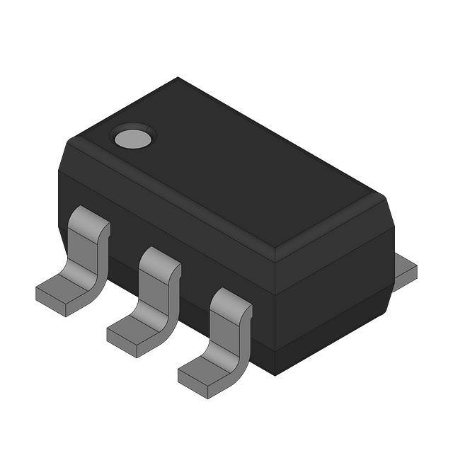
SOT-23 Package
VIN
1 µF
TPS7B4250-Q1
VOUT
3 Description
The TPS7B4250-Q1 device is a monolithic, integrated
low-dropout voltage tracker. The device is available in
a SOT-23 package. The TPS7B4250-Q1 device is
designed to supply off-board sensors in an
automotive environment. The IC has integrated
protection for overload, over temperature, reverse
polarity, and output short-circuit to the battery and
ground.
A reference voltage applied at the adjust-input pin,
ADJ, regulates supply voltages up to VIN = 45 V with
high accuracy and loads up to 50 mA.
By setting the adjust/enable input pin, ADJ/EN, to
low, the TPS7B4250-Q1 device switches to standby
mode which reduces the quiescent current to the
minimum value.
Device Information(1)
PART NUMBER
PACKAGE
TPS7B4250-Q1
SOT-23 (5)
BODY SIZE (NOM)
2.90 mm × 1.60 mm
(1) For all available packages, see the orderable addendum at
the end of the data sheet.
Output Lower than Reference Voltage
Output Equal to Reference Voltage
Vbat
Off-board Sensor Supply
High-Precision Voltage Tracking
Vreg
Vbat
VIN
1 µF
2.2 µF
TPS7B4250-Q1
VOUT
Vreg
2.2 µF
Vref
Vref
ADJ/EN
GND
ADJ/EN
GND
1
An IMPORTANT NOTICE at the end of this data sheet addresses availability, warranty, changes, use in safety-critical applications,
intellectual property matters and other important disclaimers. PRODUCTION DATA.
�TPS7B4250-Q1
SLVSCA0C – OCTOBER 2013 – REVISED SEPTEMBER 2016
www.ti.com
Table of Contents
1
2
3
4
5
6
7
Features ..................................................................
Applications ...........................................................
Description .............................................................
Revision History.....................................................
Pin Configuration and Functions .........................
Specifications.........................................................
1
1
1
2
4
5
6.1
6.2
6.3
6.4
6.5
6.6
5
5
5
5
6
7
Absolute Maximum Ratings ......................................
ESD Ratings..............................................................
Recommended Operating Conditions.......................
Thermal Information ..................................................
Electrical Characteristics...........................................
Typical Characteristics ..............................................
Detailed Description .............................................. 9
7.1
7.2
7.3
7.4
Overview ................................................................... 9
Functional Block Diagram ......................................... 9
Feature Description................................................... 9
Device Functional Modes........................................ 11
8
Application and Implementation ........................ 12
8.1 Application Information............................................ 12
8.2 Typical Application ................................................. 12
9 Power Supply Recommendations...................... 13
10 Layout................................................................... 14
10.1 Layout Guidelines ................................................. 14
10.2 Layout Example .................................................... 14
10.3 Power Dissipation and Thermal Considerations ... 15
11 Device and Documentation Support ................. 16
11.1
11.2
11.3
11.4
11.5
11.6
11.7
Device Support......................................................
Documentation Support ........................................
Receiving Notification of Documentation Updates
Community Resource............................................
Trademarks ...........................................................
Electrostatic Discharge Caution ............................
Glossary ................................................................
16
16
16
16
16
16
16
12 Mechanical, Packaging, and Orderable
Information ........................................................... 16
4 Revision History
NOTE: Page numbers for previous revisions may differ from page numbers in the current version.
Changes from Revision B (July 2015) to Revision C
Page
•
Changed the title of the data sheet ....................................................................................................................................... 1
•
Added the Device Support and Receiving Notification of Documentation Updates sections............................................... 16
Changes from Revision A (November 2013) to Revision B
Page
•
Changed HBM ESD Classification level from 2 to 3A ........................................................................................................... 1
•
Changed CDM ESD Classification level from C4 to C6 ......................................................................................................... 1
•
Added Pin Configuration and Functions section, ESD Ratings table, Feature Description section, Device Functional
Modes, Application and Implementation section, Power Supply Recommendations section, Layout section, Device
and Documentation Support section, and Mechanical, Packaging, and Orderable Information section ............................... 1
•
Deleted the transient current and 107-pF capacitor for HBM table notes from the ESD Ratings table ................................ 5
•
Changed input voltage symbol from VIN to VI for the ΔVO(ΔVI) and Vdropout parameters and the output voltage symbol
from VOUT to VO for the IL parameter in the Electrical Characteristics table ........................................................................... 6
•
Added IO and CO to the PSRR test condition in the Electrical Characteristics table ............................................................. 6
•
Changed the max value for Vdropout where IO = 10 mA from 250 to 265 in the Electrical Characteristics table ..................... 6
•
Deleted the VADJ = 5 V condition for the Ground current vs Temperature graph and changed the legend ........................... 7
•
Changed the y axis units from mV to mA in the Current-limit vs Temperature graph .......................................................... 7
•
Added the VADJ condition statement to the Input Voltage vs Output Voltage graph and changed the y-axis from IO to VO .. 7
•
Changed the title of Figure 8 from Input Voltage vs Output Voltage to Reference Voltage vs Output Voltage, and
changed the y-axis from IO to VO. Also added the VI condition statement to the graph......................................................... 7
•
Changed the second y axis from IO to VI and removed the units in the Line Transient......................................................... 7
•
Deleted the units from the second y axis in the Load Transient ............................................................................................ 7
•
Added the VADJ condition statement to the Power-supply Rejection Ratio vs Frequency graph ........................................... 8
•
Added resistor-divider values to the Tracking LDO With Enable Circuit figure.................................................................... 11
2
Submit Documentation Feedback
Copyright © 2013–2016, Texas Instruments Incorporated
Product Folder Links: TPS7B4250-Q1
�TPS7B4250-Q1
www.ti.com
SLVSCA0C – OCTOBER 2013 – REVISED SEPTEMBER 2016
Changes from Original (October 2013) to Revision A
Page
•
Changed CDM ESD Classification level from C3B to C4 throughout document ................................................................... 1
•
Changed VOUT min value from –0.3 to –1 in the Absolute Maximum Ratings table............................................................... 5
•
Added transient current flow to ESD rating in the Absolute Maximum Ratings table ............................................................ 5
•
Changed HBM absolute maximum rating from 2 kV to 4 kV.................................................................................................. 5
•
Deleted relevant ESR value from Recommended Operating Conditions table...................................................................... 5
•
Added grater-than-or-equal-to (≥) value to VADJ/EN in condition statement of the Electrical Characteristics table ................ 6
•
Added VADJ = 1.5 V to both test conditions for VUVLO parameter in the Electrical Characteristics table ................................ 6
•
Changed max value for load regulation parameter from 3 to 4 in the Electrical Characteristics table .................................. 6
•
Changed max value for the current consumption test condition where IO = 0.5 mA from 80 to 90 in the Electrical
Characteristics table ............................................................................................................................................................... 6
•
Added the Detailed Description section.................................................................................................................................. 9
•
Added the TPS7B4250 block diagram ................................................................................................................................... 9
Submit Documentation Feedback
Copyright © 2013–2016, Texas Instruments Incorporated
Product Folder Links: TPS7B4250-Q1
3
�TPS7B4250-Q1
SLVSCA0C – OCTOBER 2013 – REVISED SEPTEMBER 2016
www.ti.com
5 Pin Configuration and Functions
DBV Package
5-Pin SOT-23
Top View
ADJ/EN
1
GND
2
VIN
3
5
GND
4
VOUT
Not to scale
Pin Functions
PIN
NAME
NO.
TYPE
DESCRIPTION
ADJ/EN
1
I
This pin connects to the reference voltage. A low signal disables the IC and a high signal
enables the device. Connected the voltage reference directly or with a voltage divider for lower
output voltages. To compensate for line influences, TI recommends to place a capacitor close
to the IC pins.
GND
2
G
Internally connected to pin 5
GND
5
G
Internally connected to pin 2
VIN
3
I
This pin is the device supply. To compensate for line influences, TI recommends to place a
capacitor close to the IC pins.
VOUT
4
O
VOUT is an external capacitor that is required between VOUT and GND with respect to the
capacitance and ESR requirements given in the Recommended Operating Conditions.
4
Submit Documentation Feedback
Copyright © 2013–2016, Texas Instruments Incorporated
Product Folder Links: TPS7B4250-Q1
�TPS7B4250-Q1
www.ti.com
SLVSCA0C – OCTOBER 2013 – REVISED SEPTEMBER 2016
6 Specifications
6.1 Absolute Maximum Ratings
over operating free-air temperature range (unless otherwise noted) (1)
Input voltage, unregulated input, VIN (2) (3)
MIN
MAX
UNIT
–20
45
V
–1
22
V
–0.3
22
V
7
V
Output voltage, regulated output, VOUT
Adjust input and enable input voltage, ADJ/EN (2) (3)
ADJ Voltage minus input voltage (ADJ–VIN), VIN > 0 V
Operating junction temperature, TJ
–40
150
°C
Storage temperature, Tstg
–65
150
°C
(1)
(2)
(3)
Stresses beyond those listed under absolute maximum ratings may cause permanent damage to the device. These are stress ratings
only and functional operation of the device at these or any other conditions beyond those indicated under recommended operating
conditions is not implied. Exposure to absolute-maximum-rated conditions for extended periods may affect device reliability.
All voltage values are with respect to ground, GND.
Absolute maximum voltage.
6.2 ESD Ratings
VALUE
V(ESD)
(1)
Electrostatic discharge
Human-body model (HBM), per AEC Q100-002 (1)
±4000
Charged-device model (CDM), per AEC Q100-011
±1000
UNIT
V
AEC Q100-002 indicates that HBM stressing shall be in accordance with the ANSI/ESDA/JEDEC JS-001 specification.
6.3 Recommended Operating Conditions
over operating free-air temperature range (unless otherwise noted) (1)
MIN
MAX
4
40
V
regulated output
1.5
18
V
ADJ/EN
Adjust input and enable input voltage
1.5
18
V
ADJ–VIN
ADJ voltage minus input voltage
5
V
COUT
Output capacitor requirements (2)
1
50
µF
ESRCOUT
Output ESR requirements
0.001
20
Ω
TJ
Operating junction temperature
–40
150
°C
VIN
Unregulated input
VOUT
(1)
(2)
UNIT
Within the functional range, the IC operates as described in the circuit description. The electrical characteristics are specified within the
conditions given in the related electrical characteristics table.
The minimum output capacitance requirement is applicable for a worst-case capacitance tolerance of 30%.
6.4 Thermal Information
TPS7B4250-Q1
THERMAL METRIC
(1) (2)
DBV (SOT-23)
UNIT
5 PINS
RθJA
Junction-to-ambient thermal resistance
171.7
°C/W
RθJC(top)
Junction-to-case (top) thermal resistance
81.1
°C/W
RθJB
Junction-to-board thermal resistance
31.7
°C/W
ψJT
Junction-to-top characterization parameter
4.5
°C/W
ψJB
Junction-to-board characterization parameter
31.2
°C/W
RθJC(bot)
Junction-to-case (bottom) thermal resistance
N/A
°C/W
(1)
(2)
For more information about traditional and new thermal metrics, see the Semiconductor and IC Package Thermal Metrics application
report (SPRA953).
The thermal data is based on the JEDEC standard high K profile, JESD 51-7. Two-signal, two-plane, four-layer board with 2-oz. copper.
The copper pad is soldered to the thermal land pattern. Also, correct attachment procedure must be incorporated.
Submit Documentation Feedback
Copyright © 2013–2016, Texas Instruments Incorporated
Product Folder Links: TPS7B4250-Q1
5
�TPS7B4250-Q1
SLVSCA0C – OCTOBER 2013 – REVISED SEPTEMBER 2016
www.ti.com
6.5 Electrical Characteristics
VI = 13.5 V, 18 V ≥ VADJ/EN ≥ 1.5 V, TJ = –40ºC to 150ºC unless otherwise stated
PARAMETER
VUVLO
VIN undervoltage detection
TEST CONDITIONS
MIN
Ramp up VI until the output turns on, VADJ = 1.5 V
TYP
MAX
3.65
Ramp down VI until the output turns off, VADJ = 1.5 V
3
IO = 100 µA to 1 mA, VI = 4 V to 40 V, 1.5 V < VADJ <
VI – 0.3 V
–4
4
IO = 1 mA to 50 mA, VI = 4 V to 40 V, 1.5 V < VADJ <
VI – 1.5 V
–5
5
UNIT
V
ΔVO
Output-voltage tracking accuracy
ΔVO(ΔIL)
Load regulation steady-state
IO = 1 mA to 30 mA
ΔVO(ΔVI)
Line regulation steady-state
IO = 10 mA, VI = 6 V to 40 V
PSRR
Power-supply ripple rejection
Frequency = 100 Hz, Vrip = 0.5 VPP, IO = 5 mA, CO =
2.2 µF
Vdropout
Dropout voltage, Vdropout = VI – VQ
IL
Output-current limitation
VO short to GND
100
500
mA
IR
Reverse current at VIN
VI = 0 V, VO = 20 V, VADJ = 5 V
–5
0
µA
IRN1
Reverse current at negative input
voltage
VI = –20 V, VO = 0 V, VADJ = 5 V
–5
0
IRN2
VI = –20 V, VO = 20 V, VADJ = 5 V
–5
0
TSD
Thermal shutdown temperature
3
mV
60
dB
150
265
550
1000
TJ increasing because of power dissipation
generated by the IC
175
VADJ < 0.8 V, TA ≤ 85°C (2)
7.5
VADJ < 0.8 V, TA ≤ 125°C
Current consumption
IADJ
Adjust-input and enable-input
current
VADJ = 5 V
VADJ,low
Adjust and enable low signal valid
VO = 0 V
VADJ,high
Adjust and enable high signal valid
|VO – VADJ| < 5 mV
6
mV
(1)
IQ
(1)
(2)
4
IO = 10 mA, VI ≥ 4 V (1)
IO = 50 mA, VI ≥ 4 V
mV
µA
°C
15
20
IO = 0.5 mA, VADJ = 5 V
40
90
IO = 30 mA, VADJ = 5 V
150
350
1
1.5
mV
µA
µA
0.8
V
18
V
Measured when the output voltage VQ has dropped 10 mV from the typical value.
Ensured by design.
Submit Documentation Feedback
Copyright © 2013–2016, Texas Instruments Incorporated
Product Folder Links: TPS7B4250-Q1
�TPS7B4250-Q1
www.ti.com
SLVSCA0C – OCTOBER 2013 – REVISED SEPTEMBER 2016
6.6 Typical Characteristics
400
1000
350
900
800
300
700
250
Vdrop (mV)
Vdrop (mV)
±40ƒC
0ƒC
25ƒC
75ƒC
125ƒC
200
150
600
500
400
300
100
200
50
100
0
0
±40 ±25 ±10
5
20
35
50
65
80
95
Temperature (ƒC)
VI = VADJ = 4 V
0
110 125
5
20
25
30
35
40
45
IO (mA)
50
C002
VI = VADJ = 4 V
Figure 2. Dropout Voltage vs Output Current
250
200
VADJ