Order
Now
Product
Folder
Support &
Community
Tools &
Software
Technical
Documents
TPS80010
SLVSAD1B – JUNE 2010 – REVISED JANUARY 2016
TPS80010 PMU for Alkaline Battery-Powered Applications
1 Features
3 Description
•
•
The TPS80010 device provides an integrated powermanagement solution for 2-cell alkaline battery
applications such as wireless mice, keyboards, and
video game controllers. The VBUCK 1.8-V output is
powered by a buck converter with a load capacity of
100 mA. A Power Good (PG) signal is generated
when VBUCK is greater than 90% of its target output
voltage. Integrated in the TPS80010 is an 80-mΩ
load switch that can be connected to the VBUCK
output, allowing more system design flexibility when
connecting to multiple loads. The 3.1-V VBOOST
output is powered by a boost converter. The
VBOOST output voltage is post-regulated by the
integrated 3-V LDO. This post-regulation provides a
low-noise supply level through the specified battery
range.
1
•
•
•
•
•
•
1.8-V Buck DC-DC Converter
3.1-V Boost DC-DC Converter with 3-V PostRegulation LDO
Over 91% Conversion Efficiency
Current-Limited Start-Up for Both DC-DC
Converters
Load Switch With Current-Limited Turnon
Battery-Level Monitor Switch
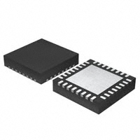
32-Pin, 4-mm × 4-mm × 1-mm VQFN Package
ESD Performance Tested per JESD 22
– 2000-V Human-Body Model
(A114-B, Class II)
– 500-V Charged-Device Model (C101)
Device Information(1)
2 Applications
•
•
•
PART NUMBER
Wireless Mice
Wireless Keyboards
Game Controllers
TPS80010
PACKAGE
VQFN (32)
BODY SIZE (NOM)
4.00 mm × 4.00 mm
(1) For all available packages, see the orderable addendum at
the end of the data sheet.
Typical Application
1.8 V–3.6 V
AA
AA
10 mF
10 mF
VIN_BOOST
BAT_FALSELOAD
VIN_BUCK
PP_BAT
10 W
10 mH
SW_BOOST
EN_BOOST
VO_BOOST
EN_LDO
FB_BOOST
3.1 V
22 mF
EN_BUCK
TPS80010
IN_VM
EN_SW1
EN_BAT_CHECK
3V
OUT_VM
4.7 mF
CONTROLLER
EN_BAT_FLASELOAD
2.2 mH
PG
SW_BUCK
OPTICAL
SENSOR
LED
1.8 V
10 mF
BAT_CHECK
MEMORY/
IO
FB_BUCK
1.8 kW
MODE_BUCK
IN_VIO
ADC
OUT_VIO
TEST1
NC
1.8 kW
1.8 V
1.8-V
PERIPHERALS
TEST2
GND
1
An IMPORTANT NOTICE at the end of this data sheet addresses availability, warranty, changes, use in safety-critical applications,
intellectual property matters and other important disclaimers. PRODUCTION DATA.
�TPS80010
SLVSAD1B – JUNE 2010 – REVISED JANUARY 2016
www.ti.com
Table of Contents
1
2
3
4
5
6
7
Features ..................................................................
Applications ...........................................................
Description .............................................................
Revision History.....................................................
Pin Configuration and Functions .........................
Specifications.........................................................
1
1
1
2
3
5
6.1
6.2
6.3
6.4
6.5
6.6
6.7
5
5
5
5
6
8
9
Absolute Maximum Ratings ......................................
ESD Ratings..............................................................
Recommended Operating Conditions.......................
Thermal Information ..................................................
Electrical Characteristics...........................................
Timing Requirements ................................................
Typical Characteristics ..............................................
Detailed Description ............................................ 11
7.1 Overview ................................................................. 11
7.2 Functional Block Diagram ....................................... 12
7.3 Feature Description................................................. 13
7.4 Device Functional Modes........................................ 14
8
Application and Implementation ........................ 15
8.1 Application Information............................................ 15
8.2 Typical Application ................................................. 15
9 Power Supply Recommendations...................... 19
10 Layout................................................................... 20
10.1 Layout Guidelines ................................................. 20
10.2 Layout Example .................................................... 20
11 Device and Documentation Support ................. 21
11.1
11.2
11.3
11.4
11.5
Device Support......................................................
Community Resources..........................................
Trademarks ...........................................................
Electrostatic Discharge Caution ............................
Glossary ................................................................
21
21
21
21
21
12 Mechanical, Packaging, and Orderable
Information ........................................................... 21
4 Revision History
NOTE: Page numbers for previous revisions may differ from page numbers in the current version.
Changes from Revision A (June 2010) to Revision B
Page
•
Added ESD Ratings table, Feature Description section, Device Functional Modes, Application and Implementation
section, Power Supply Recommendations section, Layout section, Device and Documentation Support section, and
Mechanical, Packaging, and Orderable Information section .................................................................................................. 1
•
Changed values in Thermal Information table........................................................................................................................ 5
2
Submit Documentation Feedback
Copyright © 2010–2016, Texas Instruments Incorporated
Product Folder Links: TPS80010
�TPS80010
www.ti.com
SLVSAD1B – JUNE 2010 – REVISED JANUARY 2016
5 Pin Configuration and Functions
SW_BOOST
VO_BOOST
MODE_BUCK
GND2
EN_BUCK
VIN_BUCK
SW_BUCK
GND_BUCK
RSM Package
32-Pin VQFN
Bottom View
1
32
EN_BOOST
GND_BOOST
EN_LDO
GND
VIN_BOOST
EN_BAT_CHECK
FB_BOOST
FB_BUCK
THERMAL PAD
IN_VM
BAT_FLASELOAD_EN
OUT_VM
EN_SW1
GND_FALSELOAD
BAT_FALSELOAD
PP_BAT
GND3
PG
TEST2
TEST1
IN_VIO
OUT_VIO
BAT_CHECK
OUT_VIO
IN_VIO
Pin Functions
PIN
NAME
NO.
I/O
DESCRIPTION
BAT_CHECK
15
O
Battery monitor switch output. Connect to ADC for battery-level check.
BAT_FALSELOAD
18
I
Battery monitor input for false-load check
BAT_FALSELOAD_EN
28
I
Battery false load switch enable
EN_BAT_CHECK
30
I
Battery-check path enable
EN_BOOST
32
I
Boost converter enable
EN_BUCK
4
I
Buck converter enable
EN_LDO
31
I
Boost post-regulation LDO enable
EN_SW1
27
I
Buck-load switch (SW1) enable
FB_BOOST
12
I
Boost-converter feedback input
FB_BUCK
29
I
Buck converter feedback input
GND
10
–
Ground
GND2
5
–
Device ground
GND3
20
–
Device ground
GND_BOOST
9
–
Boost converter ground
GND_BUCK
1
–
Buck converter ground
Submit Documentation Feedback
Copyright © 2010–2016, Texas Instruments Incorporated
Product Folder Links: TPS80010
3
�TPS80010
SLVSAD1B – JUNE 2010 – REVISED JANUARY 2016
www.ti.com
Pin Functions (continued)
PIN
NAME
GND_FALSELOAD
NO.
I/O
DESCRIPTION
17
O
False load ground
IN_VIO
25, 26
–
Internal I/O power supply. Load switch 1 input. Connect externally to buck output
IN_VM
13
I
Boost post-regulation LDO input. Connect externally to VO_BOOST.
MODE_BUCK
6
I
Buck converter mode control. High for PWM, low for PFM.
OUT_VIO
23, 24
O
Load switch 1 output
OUT_VM
14
O
Boost post-regulation LDO output
PG
21
O
Buck Power Good indication output. High when VBUCK > 1.7 V.
PP_BAT
19
I
Battery input for level check
SW_BOOST
8
I/O
Boost converter switching node. Inductor connection.
SW_BUCK
2
O
Buck converter switching output. Inductor connection.
TEST1
22
I/O
Test pin1 (tie to GND)
TEST2
16
O
Test pin 2 (do not connect)
VIN_BOOST
11
–
Boost-converter power supply
VIN_BUCK
3
–
Buck converter power supply
VO_BOOST
7
O
Boost converter regulated output
4
Submit Documentation Feedback
Copyright © 2010–2016, Texas Instruments Incorporated
Product Folder Links: TPS80010
�TPS80010
www.ti.com
SLVSAD1B – JUNE 2010 – REVISED JANUARY 2016
6 Specifications
6.1 Absolute Maximum Ratings
over operating free-air temperature range (unless otherwise noted) (1)
MIN
MAX
UNIT
VI
Input voltage (all pins)
–0.3
3.6
V
VO
Output voltage (all pins)
–0.3
3.6
V
TJ
Junction temperature
–40
125
°C
Tstg
Storage temperature
–65
150
°C
(1)
Stresses beyond those listed under Absolute Maximum Ratings may cause permanent damage to the device. These are stress ratings
only, and functional operation of the device at these or any other conditions beyond those indicated under Recommended Operating
Conditions is not implied. Exposure to absolute-maximum-rated conditions for extended periods may affect device reliability.
6.2 ESD Ratings
V(ESD)
(1)
(2)
Electrostatic discharge
Human body model (HBM), per ANSI/ESDA/JEDEC JS-001, all pins (1)
Charged device model (CDM), per JEDEC specification JESD22-C101, all pins
(2)
MAX
UNIT
±2000
V
±500
V
JEDEC document JEP155 states that 500-V HBM allows safe manufacturing with a standard ESD control process.
JEDEC document JEP157 states that 250-V CDM allows safe manufacturing with a standard ESD control process.
6.3 Recommended Operating Conditions
TA = 0°C to 85°C; typical values are at TA = 25°C
MIN
VBAT
Input voltage, VIN BOOST, VIN_BUCK, PP_BAT pins
VIO (IN_VIO)
Digital I/O operating voltage
TA
Ambient temperature
NOM
1.95
MAX
UNIT
3.6
V
1.8
VBAT
V
25
85
°C
0
6.4 Thermal Information
TPS80010
THERMAL METRIC (1)
RSM (VQFN)
UNIT
32 PINS
RθJA
Junction-to-ambient thermal resistance
37.4
°C/W
RθJC(top)
Junction-to-case (top) thermal resistance
31.8
°C/W
RθJB
Junction-to-board thermal resistance
8.2
°C/W
ψJT
Junction-to-top characterization parameter
0.4
°C/W
ψJB
Junction-to-board characterization parameter
8.2
°C/W
RθJC(bot)
Junction-to-case (bottom) thermal resistance
2.5
°C/W
(1)
For more information about traditional and new thermal metrics, see the Semiconductor and IC Package Thermal Metrics application
report, SPRA953.
Submit Documentation Feedback
Copyright © 2010–2016, Texas Instruments Incorporated
Product Folder Links: TPS80010
5
�TPS80010
SLVSAD1B – JUNE 2010 – REVISED JANUARY 2016
www.ti.com
6.5 Electrical Characteristics
TA = 0°C to 85°C; typical values are at TA = 25°C (unless otherwise noted)
PARAMETER
TEST CONDITIONS
MIN
TYP
MAX
UNIT
SUPPLY CURRENT
IQ
Quiescent current
VBAT = 3 V, all modules enabled
IOFF
Off current
VBAT = 3 V
RPULLDOWN
Internal pulldown resistor
EN_BOOST, EN_LDO, EN_SW1,
EN_BAT_CHECK, EN_BAT_FALSELOAD
157
VIH
Input logic-high voltage
EN_BOOST, EN_LDO, EN_SW1,
EN_BAT_CHECK, EN_BAT_FALSELOAD
0.7 × VIO
51
μA
1
μA
DIGITAL I/O
EN_BUCK, BUCK_MODE
VIL
Input logic-low voltage
275
V
0.3 × VIO
0.7 ×
VBAT
EN_BUCK, BUCK_MODE
Output logic-high voltage
PG
VOL
Output logic-low voltage
PG
IL_DIG
Logic-output load current
kΩ
0.7 × VBAT
EN_BOOST, EN_LDO, EN_SW1,
EN_BAT_CHECK, EN_BAT_FALSELOAD
VOH
383
VIO – 0.2
V
V
0.2
1
V
mA
BUCK CONVERTER
VIN
Input voltage at VIN_BUCK
IO
Output current
VFB
Feedback voltage (output
accuracy)
VBUCK
Buck output voltage
ISW
Switch current limit
IRUSH
Inrush current
Line regulation
Load regulation
Efficiency
Quiescent current
1.95
PWM, IO = 0 mA to 100 mA,
VIN ≥ 1.85 V to 3.6 V, VBUCK = 1.8 V
–1.5%
PFM
V
100
mA
1.5%
1
1.8
0.56
VIN = 2 V
0.7
V
0.84
150
PWM, IO = 100 mA
A
mA
0.9%
PFM, IO = 100 mA
0.9%
PWM, VIN = 2.4 V, IO = 0 mA to 100 mA
–0.5%
PFM, VIN = 2.4 V, IO = 0 mA to 100 mA
0.5%
PFM , IO = 100 mA, VIN = 2.4 V, VBUCK = 1.8 V
92%
PWM, IO = 100 mA, VIN = 2.4 V, VBUCK = 1.8 V
90%
PFM, IO = 0 mA, no switching
21
PFM, IO = 0 mA, switching
25
PWM, IO = 0 mA
IQ
3.6
μA
5
Shutdown current
Leakage current into
SW_BUCK
mA
0.005
0.15
μA
0.01
1
μA
RREC
Rectifier on-resistance
VGS = 3.6 V
185
380
mΩ
RMAIN
Main SW on-resistance
VGS = 3.6 V
240
480
mΩ
ΔVLN
Line transient output variation
PFM, IO = 50 mA, VIN = 2 V → 3.6 V, Δt = 25 µs
10
20
mV
ΔVLD
PFM, VIN = 2.4 V, VBUCK = 1.8 V,
Load transient output variation
IO = 1 mA → 100 mA, Δt = 1 µs
30
40
mV
VRIP
Output ripple
fSW
Switching frequency
UVLO
Undervoltage lockout
threshold
1.7
V
CL
Load capacitance
10
μF
L
Inductor
2.2
μH
6
PWM, IO = 100 mA, VIN = 2.4 V
PFM, IO = 10 mA, VIN = 3.6 V
2
Submit Documentation Feedback
1
10
10
20
2.25
2.5
mVpp
MHz
Copyright © 2010–2016, Texas Instruments Incorporated
Product Folder Links: TPS80010
�TPS80010
www.ti.com
SLVSAD1B – JUNE 2010 – REVISED JANUARY 2016
Electrical Characteristics (continued)
TA = 0°C to 85°C; typical values are at TA = 25°C (unless otherwise noted)
PARAMETER
TEST CONDITIONS
MIN
TYP
MAX
UNIT
80
120
mΩ
360
mA
100
mA
1
μA
1.7
1.72
V
10
15
LOAD SWITCH
RON
Switch on-resistance
VGS = 1.8 V
Maximum load current
Turnon inrush current
IOFF
Off-state current
Switch turned off, IO = 0 mA
POWER GOOD RESET
VTHRESH
Power good threshold voltage
VHYS
Power good hysteresis
1.68
mV
BOOST CONVERTER
Boost mode
1.8
3.1
VIN > VBOOST mode, VBOOST = VIN
3.1
3.6
VIN
Input voltage at VIN_BOOST
VBOOST
Output voltage
TA = 0°C–50°C, VIN = 1.8 V to 3.1 V,
IO = 0 mA to 50 mA
IO
Output current
VIN = 1.8 V to 3.6 V
ISW
Switch current limit
IRUSH
Inrush current
VIN = 2 V
RREC
Rectifier on-resistance
VBOOST = 3.1 V
RMAIN
Main SW on-resistance
fSW
3
200
3.1
350
V
50
mA
475
mA
mA
1
Ω
1
Ω
Line regulation
VIN = 2 V to 3 V, IO = 50 mA
0.5%
Load regulation
VIN = 2 V, IO = 0–50 mA
0.5%
Boost efficiency
VIN = 2.4 V, IO = 5 mA
91%
Oscillator frequency
3.2
150
VIN = 2.4 V, IO = 50 mA
91
kHz
625
From VIN supply, IO = 0 mA, VIN = 1.8 V,
VBOOST = 3.1 V
1
2.5
From VBOOST, IO = 0 mA, VIN = 1.8 V,
VBOOST = 3.1 V
4
6.5
Shutdown current
0.1
1
Leakage current into
SW_BOOST
0.1
1
VUVLO
VIN decreasing
0.5
0.7
ΔVLN
Line transient output variation
ΔVLD
V = 2.4 V, VBOOST = 3.1 V, IO = 1 mA → 50 mA,
Load transient output variation IN
Δt = 1 µs
VRIP
Output ripple
IOFF
Off-mode current
CL
Load capacitance
L
Inductance
Quiescent current
IQ
IO = 10 mA, VIN = 1.8 V → VBOOST, ΔT = 25 µs
10
VIN = 1.8 V, IO = 50 mA
6
V
μA
V
mV
5
10
4
10 mVpp
0.1
1
10
22
10
mV
μA
μF
μH
POST REGULATION LDO
VIN
Input voltage at IN_VM
VLDO
Output voltage
10 µA ≤ IO ≤ IOMAX
3.6
V
2.91
3.1
3
3.09
V
IO
Output current
Normal mode
ILIMIT
Current limit
VLDO > 1 V
50
mA
300
400
500
ISHORT
Short circuit current
Output shorted to ground
mA
30
60
150
mA
VREG
Line regulation
dVLDO/dVIN at IO = Max
LREG
Load regulation
VLDO (IOMIN) – VLDO(IOMAX)
40
mV
ΔVLN
Load transient response
IO = 20 mA/µs, VIN = 3.1 V
50
100
mV
IQ
Quiescent current
IO = 0 mA
16
17.6
µA
0.2%
Submit Documentation Feedback
Copyright © 2010–2016, Texas Instruments Incorporated
Product Folder Links: TPS80010
7
�TPS80010
SLVSAD1B – JUNE 2010 – REVISED JANUARY 2016
www.ti.com
Electrical Characteristics (continued)
TA = 0°C to 85°C; typical values are at TA = 25°C (unless otherwise noted)
PARAMETER
TEST CONDITIONS
MIN
TYP
MAX
UNIT
PSRR
Power-supply ripple rejection
f = 120 Hz to 1 kHz at IO = IOMAX/2, VIN = 3.1 V
VRIP_NORM
Output ripple
VBAT < 3.1 V, IO = 50 mA, VIN = VBOOST
0.1
1 mVpp
VRIP_HIBAT
Output ripple
VBAT > 3.1 V, IO = 50 mA, VIN = VBOOST
4
10 mVpp
Boost plus LDO efficiency
CL
Load capacitance
40
VBAT = 2.4 V, IO = 5 mA, VIN = VBOOST
dB
87%
VBAT = 2.4 V, IO = 50 mA, VIN = VBOOST
88%
Ceramic capacitor, ESR = 10 mΩ to 150 mΩ
4.7
10
22
µF
1.8
3.6
V
3.6
V
VIN
V
BATTERY LOAD MONITOR
VOP
Operating voltage
VIN
Input voltage at PP_BAT
VOUT
Output voltage at
BAT_CHECK
ILOAD
Load current
RON
Switch on-resistance
1.8
VIN = 1.8 V to 3.6 V
10
mA
12
15
Ω
1.8
3.6
V
3.6
V
BATTERY LOAD SWITCH
VOP
Operating voltage
VIN
Input voltage at
BAT_FALSELOAD
IIN
Input current
RON
Switch on-resistance
240
360
mA
500
mΩ
6.6 Timing Requirements
MIN
NOM
MAX
UNIT
BUCK CONVERTER
tSTART
Start-up time
10
ms
LOAD SWITCH
4
ms
tON
Output rise time; 10%–90% of final VO, CL = 100 µF
Turnon time; CL = 100 µF
2
6
ms
tOFF
Turnoff time; CL = 100 µF
10
ms
150
200
ms
0.25
10
ms
POWER GOOD RESET
ΔtPG
Power good time-out delay
100
BOOST CONVERTER
tSTART
Start-up time; from enable, VBOOST = 10% → 90%
POST REGULATION LDO
tON
Turn-on time; IO = 0 mA, VLDO = 90%, CL = 2.9 µF
130
500
µs
tOFF
Turn-off time; IO = 0 mA, VLDO < 0.5 V, CL = 2.9 µF
3.9
5
ms
8
Submit Documentation Feedback
Copyright © 2010–2016, Texas Instruments Incorporated
Product Folder Links: TPS80010
�TPS80010
www.ti.com
SLVSAD1B – JUNE 2010 – REVISED JANUARY 2016
6.7 Typical Characteristics
1.830
95
1.825
VBUCK - Buck Output Voltage - V
100
Efficiency - %
90
85
VIN = 2.1 V
VIN = 2.4 V
80
VIN = 2.8 V
75
VIN = 3.2 V
70
VIN = 3.2 V
1.820
1.815
VIN = 2.8 V
1.810
1.805
VIN = 2.4 V
1.800
VIN = 2.1 V
1.795
65
1.790
60
0.1
1
10
Load - mA
100
Figure 1. Buck Efficiency, MODE_BUCK = 0
0
10
20
30
40 50 60
Load - mA
70
80
90
100
Figure 2. Buck Output Voltage vs Load, MODE_BUCK = 0
1.805
VBUCK - Buck Output Voltage - V
VIN = 2.4 V
Iload = 100 mA
VIN = 3.2 V
1.803
VIN = 2.8 V
VIN = 2.4 V
1.801
1.799
VBUCK
VIN = 2.1 V
1.797
10 mV/div
1 ms/div
1.795
0
20
40
60
Load - mA
80
100
Figure 4. Buck Output-Voltage Ripple, PWM
Figure 3. Buck Output Voltage vs Load, MODE_BUCK = 1
100
VBUCK
VIN = 2.4 V
Iload = 20 mA
VIN = 3.2 V
95
VIN = 2.8 V
Efficiency - %
90
85
VIN = 2.4 V
80
75
VIN = 2.1 V
70
10 mV/div
10 ms/div
65
60
0.1
Figure 5. Buck Output-Voltage Ripple, PFM
1
Load - mA
10
100
Figure 6. Boost With LDO Efficiency
Submit Documentation Feedback
Copyright © 2010–2016, Texas Instruments Incorporated
Product Folder Links: TPS80010
9
�TPS80010
SLVSAD1B – JUNE 2010 – REVISED JANUARY 2016
www.ti.com
Typical Characteristics (continued)
VIN = 2.4 V
Iload = 50 mA
VIN = 2.4 V
Iload = 0 mA
VBOOST
VBOOST
VLDO
VLDO
10 mV/div
1 ms/div
10 mV/div
1 ms/div
Figure 7. Boost Output Voltage Ripple
Inductor
Voltage
Figure 8. Boost Output Voltage Ripple
VIN = 1.8 V to 3.1 V
Iload = 10 mA
1 V/div
10 mV/div
400 ns/div
VBOOST
Figure 9. Boost Switching Waveform,
Continuous-Current Mode
10
Submit Documentation Feedback
Figure 10. Boost Switching Waveform,
Discontinuous-Current Mode
Copyright © 2010–2016, Texas Instruments Incorporated
Product Folder Links: TPS80010
�TPS80010
www.ti.com
SLVSAD1B – JUNE 2010 – REVISED JANUARY 2016
7 Detailed Description
7.1 Overview
The TPS80010 provides a system level solution for 2-cell alkaline battery applications. Popular applications
include handheld devices including wireless mice, keyboards, and video game controllers. The TPS80010
provides two DC-DC converters, a load switch, post-regulation LDO, and battery monitoring switch—each with
their own enable pins to allow for maximum flexibility.
The buck converter operates at a fixed voltage, 1.8 V, and can provide up to 150 mA load. Automatic switching is
implemented to maximize power efficiency. In moderate to heavy loads the converter operates in PWM mode; as
load current decreases it switches to PFM mode. PWM can be forced regardless of load size by disabling this
power save mode (PFM mode). The buck allows for several loads to be connected to its output, due to the power
distributing load switch connected externally to the output of the buck.
The boost converter regulates at a fixed voltage of 3.1 V, and can provide up to 50 mA load current. It contains a
discontinuous current mode to maintain efficiency at low load currents. The boost provides a low noise supply at
low input voltages due to a post regulation LDO.
The battery monitoring switch is used to check battery lifetime. Using a false load implementation and the battery
voltage it can determine the battery impedance and therefore health.
Submit Documentation Feedback
Copyright © 2010–2016, Texas Instruments Incorporated
Product Folder Links: TPS80010
11
�TPS80010
SLVSAD1B – JUNE 2010 – REVISED JANUARY 2016
www.ti.com
7.2 Functional Block Diagram
BUCK
VIN_BUCK
EN_BUCK
MODE_BUCK
Switching
Control
SW_BUCK
GND_BUCK
+
PFM
Soft Start
-
GND
FB_BUCK
+
+
ErrAmp
-
PWM
-
VREF
PG
-
PG
Comp
1.7V
+
BUCK LOAD SW
EN_SW1
IN_VIO
Soft Turn ON
OUT_VIO
OUT_VM
ErrAmp
VREF
+
IN_VM
EN_LDO
BOOST REG. LDO
FB_BOOST
ErrAmp
+
VREF
VO_BOOST
EN_BOOST
TEST1
Regulation
&
Switching
Mode
Control
with
Soft Start
SW_BOOST
+
TEST2
I SENSE
-
GND_BOOST
VIN_BOOST
+
VIN
COMP
-
BOOST
VTH
PP_BAT
EN_BAT_CHECK
BATT
MONITOR
SWITCH
BAT_CHECK
VIO
L/S
BAT_FALSELOAD
VIO
EN_BAT_FALSELOAD
12
BATTERY
LOAD
SWITCH
Submit Documentation Feedback
GND_FALSELOAD
Copyright © 2010–2016, Texas Instruments Incorporated
Product Folder Links: TPS80010
�TPS80010
www.ti.com
SLVSAD1B – JUNE 2010 – REVISED JANUARY 2016
7.3 Feature Description
7.3.1 Enable
The TPS80010 includes two DC-DC converters, a load switch, post-regulation LDO, and battery monitoring
switch. Each of these circuits has a dedicated enable pin with an internal pulldown resistor, RPULLDOWN, that can
be driven by standard logic or by an open-drain driver. The EN_BUCK pin not only enables the buck converter,
but also serves as the master enable for the device. No other circuitry in the TPS80010 can operate without
EN_BUCK set high.
7.3.2 Buck DC-DC Converter and Load Switch
The synchronous step-down (buck) converter in the TPS80010 provides a fixed 1.8-V output with a load capacity
of 150 mA. This converter operates with a fixed switching frequency of 2.25 MHz during pulse-width-modulation
(PWM) operation at moderate to heavy loads. As the load current decreases, the converter automatically
switches to a power-save mode and operates in pulse-frequency-modulation (PFM) mode to maximize power
efficiency. During PFM operation, the converter positions the output at a voltage about 1% greater than the
nominal output voltage. This feature minimizes the output voltage drops during sudden load transients. The
power-save mode can be disabled by setting the MODE_BUCK pin high.
The buck converter has internal soft-start circuitry that limits the inrush current during startup to 150 mA, allowing
a slow and controlled output-voltage ramp. Once the output voltage reaches 1.7 V, the output monitoring circuitry
generates a Power Good (PG) output signal.
The TPS80010 also includes a load switch that is to be connected externally to the buck output voltage. This
switch provides flexibility in the design and power distribution of the end application by allowing several loads
(such as memory, I/O, Bluetooth, and so forth) to be connected to the same supply while being able to power
down or disconnect some of these loads selectively when the end application goes to a low-power mode of
operation. This switch has a controlled turnon to limit the inrush current caused by the load, and hence the load
transient to the buck converter.
7.3.3 Boost DC-DC Converter and Post-Regulation LDO
The TPS80010 includes a synchronous step-up (boost) converter that provides a 3.1-V fixed output at 50-mA
load current. The boost converter is controlled by a hysteretic current-mode controller. This controller regulates
the output voltage by keeping the inductor ripple current constant and adjusting the offset of this inductor current
depending on the output load. If the required average input current is lower than the average inductor current
defined by this constant ripple, the converter goes into discontinuous-current mode (DCM) to keep the efficiency
high at low-load conditions. The boost also has a soft-start circuit that limits the inrush current to 150 mA.
To provide a clean, low-noise supply when VBAT > 3.1 V, the output of the boost is post-regulated by a
3-V LDO. This post-regulation allows the TPS80010 to provide a solid 3-V supply rail to the end application
across the full input or battery-voltage range while minimizing the number of external components. To minimize
power loss through the power path, the LDO allows for 100-mV input-voltage headroom at 50-mA load.
7.3.4 Battery Monitoring Switch and False Load
The TPS80010 implements a battery-voltage monitor switch to briefly check battery lifetime. The integrated falseload switch connects a specified load to the battery. When this false load is applied, the battery monitor switch is
turned on, gating the sensed battery voltage to the ADC in the system. Based on this measurement, the system
can determine the battery impedance and, therefore, battery health.
Submit Documentation Feedback
Copyright © 2010–2016, Texas Instruments Incorporated
Product Folder Links: TPS80010
13
�TPS80010
SLVSAD1B – JUNE 2010 – REVISED JANUARY 2016
www.ti.com
7.4 Device Functional Modes
The step-down converter has two modes of operations to maximize efficiency: Pulse frequency modulation
(PFM) and pulse width modulation (PWM).
PFM mode is for:
• Light loads
• Automatic transition from this mode to PWM mode automatically when MODE_BUCK pin is pulled low
• Increasing output voltage setting by 1%
• Better accuracy
PWM mode is for:
• Moderate to heavy loads
• Small output ripple
• Pulling MODE_BUCK pin high to result in PWM mode over all load range
14
Submit Documentation Feedback
Copyright © 2010–2016, Texas Instruments Incorporated
Product Folder Links: TPS80010
�TPS80010
www.ti.com
SLVSAD1B – JUNE 2010 – REVISED JANUARY 2016
8 Application and Implementation
NOTE
Information in the following applications sections is not part of the TI component
specification, and TI does not warrant its accuracy or completeness. TI’s customers are
responsible for determining suitability of components for their purposes. Customers should
validate and test their design implementation to confirm system functionality.
8.1 Application Information
The TPS80010 is ideal for dual-cell alkaline battery-powered and noise-sensitive applications. The application
controller has the ability to enable resources on the power management IC to allow for maximum flexibility. The
device resources are often used to power memory, IO, and optical sensors. These devices are common in
wireless keyboards and video game controllers.
8.2 Typical Application
1.8 V–3.6 V
AA
AA
10 mF
10 mF
VIN_BOOST
BAT_FALSELOAD
VIN_BUCK
PP_BAT
10 W
10 mH
SW_BOOST
EN_BOOST
VO_BOOST
EN_LDO
FB_BOOST
3.1 V
22 mF
EN_BUCK
TPS80010
IN_VM
EN_SW1
EN_BAT_CHECK
3V
OUT_VM
4.7 mF
CONTROLLER
EN_BAT_FLASELOAD
2.2 mH
PG
SW_BUCK
OPTICAL
SENSOR
LED
1.8 V
10 mF
BAT_CHECK
MEMORY/
IO
FB_BUCK
1.8 kW
MODE_BUCK
IN_VIO
ADC
OUT_VIO
TEST1
NC
1.8 V
1.8-V
PERIPHERALS
TEST2
1.8 kW
GND
Figure 11. TPS80010 Typical Application Diagram
8.2.1 Design Requirements
The design requirements for TPS80010 are located in Table 1.
Table 1. TPS80010 Design Requirements
RESOURCE
VOLTAGE
Buck
1.8 V
Boost
3.1 V
Submit Documentation Feedback
Copyright © 2010–2016, Texas Instruments Incorporated
Product Folder Links: TPS80010
15
�TPS80010
SLVSAD1B – JUNE 2010 – REVISED JANUARY 2016
www.ti.com
8.2.2 Detailed Design Procedure
8.2.2.1 Buck Output Filter Design
The TPS80010 buck regulator is designed to operate with inductors in the range of 1.5 µH to 4.7 µH and with
output capacitors in the range of 4.7 µF to 22 µF. The part is optimized for operation with a 2.2-µH inductor and
10-µF output capacitor.
Larger or smaller inductor values can be used to optimize the performance of the device for specific operation
conditions. For stable operation, the L and C values of the output filter must not be less than 1-µH effective
inductance and 3.5-µF effective capacitance.
8.2.2.2 Buck Inductor Selection
The inductor value has a direct effect on the ripple current. The selected inductor must be rated for its DC
resistance and saturation current. The inductor ripple current (ΔIL) decreases with higher inductance and
increases with higher VIN or VBUCK.
The inductor selection also has an impact on the output-voltage ripple in PFM mode. Higher inductor values lead
to lower output-voltage ripple and higher PFM frequency; lower inductor values lead to a higher output-voltage
ripple but lower PFM frequency.
Equation 1 calculates the maximum inductor current in PWM mode under static load conditions. The saturation
current of the inductor must be rated higher than the maximum inductor current, as calculated with Equation 2.
This is recommended because during heavy load transients, the inductor current rises above the calculated
value.
V
1- BUCK
VIN
ΔIL = VBUCK ´
L ´ f
(1)
ΔIL
ILmax = IOmax +
2
where
•
•
•
•
f = Switching frequency (2.25 MHz typical)
L = Inductor value
ΔIL = Peak-to-peak inductor ripple current
ILmax = Maximum inductor current
(2)
A more conservative approach is to select the inductor current rating just for the switch current limit, ILIMF, of the
converter.
Accepting larger values of ripple current allows the use of lower inductance values, but results in higher output
voltage ripple, greater core losses, and lower output current capability.
The total losses of the coil have a strong impact on the efficiency of the DC-DC conversion and consist of both
the losses in the DC resistance (R(DC)) and the following frequency-dependent components:
• The losses in the core material (magnetic hysteresis loss, especially at high switching frequencies)
• Additional losses in the conductor from the skin effect (current displacement at high frequencies)
• Magnetic field losses of the neighboring windings (proximity effect)
• Radiation losses
8.2.2.3 Buck Output Capacitor Selection
The advanced fast-response voltage mode control scheme of the TPS80010 buck regulator allows the use of tiny
ceramic capacitors. Ceramic capacitors with low ESR values have the lowest output voltage ripple and are
recommended. The output capacitor requires either an X7R or X5R dielectric. Y5V- and Z5U-dielectric
capacitors, aside from their wide variation in capacitance over temperature, become resistive at high frequencies.
At nominal load current, the device operates in PWM mode and the RMS ripple current is calculated with
Equation 3.
16
Submit Documentation Feedback
Copyright © 2010–2016, Texas Instruments Incorporated
Product Folder Links: TPS80010
�TPS80010
www.ti.com
SLVSAD1B – JUNE 2010 – REVISED JANUARY 2016
VBUCK
VIN
1
´
L ´ f
2 ´ 3
1 IRMSCout = VBUCK ×
(3)
At nominal load current, the device operates in PWM mode and the overall output voltage ripple is the sum of the
voltage spike caused by the output capacitor ESR plus the voltage ripple caused by charging and discharging the
output capacitor in Equation 4.
V
1- BUCK
æ
ö
VIN
1
ΔVBUCK = VBUCK ×
+ ESR ÷
´ ç
L ´ f
è 8 × COUT ´ f
ø
(4)
At light-load currents, the converter operates in power-save mode, and the output-voltage ripple depends on the
output-capacitor and inductor values. Larger output-capacitor and inductor values minimize the voltage ripple in
PFM mode and tighten DC output accuracy in PFM mode.
8.2.2.4 Buck Input Capacitor Selection
An input capacitor is required for best input voltage filtering and for minimizing the interference with other circuits
caused by high input-voltage spikes. For most applications, a 4.7-µF to 10-µF ceramic capacitor is
recommended. Because a ceramic capacitor loses up to 80% of its initial capacitance at 5 V, TI recommends
that 10-µF input capacitors be used for input voltages > 4.5 V. The input capacitor can be increased without any
limit for better input-voltage filtering. Take care when using only small ceramic input capacitors. When a ceramic
capacitor is used at the input and the power is being supplied through long wires, such as from a wall adapter, a
load step at the output or VIN step on the input can induce ringing at the VIN_BUCK pin. This ringing can couple
to the output and be mistaken as loop instability or could even damage the part by exceeding the maximum
ratings.
Table 2. Recommended Component List for Buck Converter
COMPONENT
VALUE
PART
SUPPLIER
SIZE
LQM2HPN2R2MJ0L
Murata
2.5 mm × 2 mm × 1.2 mm
(1008)
Inductor
2.2 μH
LPS3015-222ML
Coilcraft
3 mm × 3 mm × 1.5 mm
Cacitor (IN)
10 μF
GRM188R60J106ME47D
Murata
0603
Capacitor (OUT)
10 μF
GRM188R60J106ME47D
Murata
0603
8.2.2.5 Boost Inductor Selection
To ensure proper operation of the TPS80010 boost DC-DC converter, a suitable inductor must be connected
between pins VIN_BOOST and SW_BOOST. Inductor values of 4.7 μH show good performance over the whole
input and output voltage range.
Choosing other inductance values affects the switching frequency f proportional to 1/L as shown in Equation 5.
V ´ (VBOOST - VIN )
1
L=
´ IN
f ´ 200 mA
VBOOST
(5)
Choosing inductor values higher than 4.7 μH can improve efficiency due to reduced switching frequency and
correspondingly reduced switching losses. Using inductor values less than 2.2 μH is not recommended.
Having selected an inductance value, the peak current for the inductor in steady-state operation can be
calculated. Equation 6 gives the peak current estimate.
ìV
ü
× IBOOST
IL,MAX = í BOOST
+ 100 mA ý
0.8 × VIN
î
þ
IL,MAX = 200 mA
continuous current operation
discontinuous current operation
(6)
IL,MAX is the required minimum inductor-current rating. The load-transient or overcurrent conditions may require
an even higher current rating.
Submit Documentation Feedback
Copyright © 2010–2016, Texas Instruments Incorporated
Product Folder Links: TPS80010
17
�TPS80010
SLVSAD1B – JUNE 2010 – REVISED JANUARY 2016
www.ti.com
The condition in Equation 7 provides an easy way to determine whether the device is in continuous or
discontinuous operation. As long as the condition is true, the device operates in continuous-current mode. If the
condition becomes false, discontinuous-current operation is established.
VBOOST × IO
> 0.8 ´ 100 mA
VIN
(7)
Due to the use of current hysteretic control in the TPS80010 boost, the series resistance of the inductor can
impact the operation of the main switch. There is a simple calculation that can ensure proper operation of the
TPS80010 boost converter. The relationship between the series resistance (RIN), the input voltage (VIN), and the
switch current limit (ISW) is shown in Equation 8.
V
RIN < IN
ISW
(8)
Examples include Equation 9 and Equation 10.
ISW = 400 mA, VIN = 2.5 V
(9)
In Equation 9, RIN < 2.5 V / 400 mA; therefore, RIN must be less than 6.25 Ω.
ISW = 400 mA, VIN = 1.8 V
(10)
In Equation 10, RIN < 1.8 V / 400 mA; therefore, RIN must be less than 4.5 Ω.
8.2.2.6 Boost Input Capacitor
The input capacitor must be at least 10 μF to improve transient behavior of the regulator and EMI behavior of the
total power-supply circuit. The input capacitor must be a ceramic capacitor and be placed as close as possible to
the VIN_BOOST and GND pins of the IC. These capacitors must be X7R or X5R ceramic capacitors.
8.2.2.7 Boost Output Capacitor
For the output capacitor COUT, TI recommends using small X7R or X5R ceramic capacitors placed as close as
possible to the VO_BOOST and GND pins of the IC. If, for any reason, the application requires the use of large
capacitors which cannot be placed close to the IC, the use of a small ceramic capacitor with a capacitance value
of around 4.7 μF in parallel with the larger one is recommended. This small capacitor must be placed as close as
possible to the VO_BOOST and GND pins of the IC.
A minimum effective capacitance value of 6 μF must be used; 10 μF is recommended. If the inductor value
exceeds 4.7 μH, the value of the effective output capacitance value must be half the inductance value or higher
for stability reasons; see Equation 11.
L
mF
COUT ³
´
2
mH
(11)
NOTE
When choosing the output capacitor, be aware of the effects of bias voltage, temperature,
and tolerance on the effective capacitance of the component. A capacitor in a 0603
package size suffers more capacitance degradation than a 0805 package at a similar bias
voltage. For example, either a 22-µF 0603-sized capacitor or a 10-µF 0805-sized
capacitor is required to work with a nominal 10-µH inductor.
The TPS80010 boost is not sensitive to ESR in terms of stability. Using low-ESR capacitors, such as ceramic
capacitors, is recommended to minimize output-voltage ripple. If heavy load changes are expected, the output
capacitor value must be increased to avoid output voltage drops during fast load transients.
Table 3. Recommended Component List for Boost Converter
COMPONENT
Inductor
18
VALUE
10 μH
PART
SUPPLIER
SIZE
CBC3225T100MR
Taiyo Yuden
3.2 mm × 2.5 mm × 2.5 mm
(1210)
DO3314-103ML
Coilcraft
3.3 mm × 3.3 mm × 1.4 mm
Submit Documentation Feedback
Copyright © 2010–2016, Texas Instruments Incorporated
Product Folder Links: TPS80010
�TPS80010
www.ti.com
SLVSAD1B – JUNE 2010 – REVISED JANUARY 2016
Table 3. Recommended Component List for Boost Converter (continued)
COMPONENT
VALUE
PART
SUPPLIER
SIZE
Capacitor (IN)
10 μF
GRM188R60J106ME47D
Murata
0603
Capacitor (OUT)
22 μF
AMK107BJ226MA-T
Taiyo Yuden
0603
8.2.3 Application Curves
VIN = 2 V to 3.6 V in 25 ms
Iload = 50 mA
VIN
1 V/div
VBUCK
20 mV/div
400 ms/div
Figure 12. Buck Output Load Transient Response
Figure 13. Buck Output Line Transient Response
VIN = 1.8 V to 3.1 V
Iload = 10 mA
VBOOST
VIN
10 mV/div
1 V/div
2 ms/div
Figure 14. Boost Line Transient Response
Figure 15. Boost Load Transient Response
9 Power Supply Recommendations
The TPS80010 was originally designed for dual-cell alkaline battery applications. Therefore, the device has
working input voltage ranges from 1.95 V to 3.6 V. As long as the input voltage range is followed, the input
supply can be from other regulated supplies.
Submit Documentation Feedback
Copyright © 2010–2016, Texas Instruments Incorporated
Product Folder Links: TPS80010
19
�TPS80010
SLVSAD1B – JUNE 2010 – REVISED JANUARY 2016
www.ti.com
10 Layout
10.1 Layout Guidelines
The VIN_BOOST and VIN_BUCK pins must be bypassed to ground with a low-ESR ceramic bypass capacitor.
Texas Instruments recommends the typical bypass capacitance is 10 μF.
• The optimum placement is closest to the VIN_BUCK and VIN_BOOST pins of the device. Minimize the loop
area formed by the bypass capacitor connection, the VINDCDC and VINLDO pins, and the thermal pad of the
device.
• The thermal pad must be tied to the PCB ground plane with multiple vias.
• The FB _BOOST, FB_BUCK, SW_BOOST, SW_BCUK, and OUT_VM pins (feedback and output pins) traces
must be routed away from any potential noise source to avoid coupling.
• Output capacitance must be placed immediately at the output pins. Excessive distance from the capacitance
to output pins may cause poor converter performance.
10.2 Layout Example
PowerPAD
vias to
GND plane
Figure 16. TPS80010 Layout
20
Submit Documentation Feedback
Copyright © 2010–2016, Texas Instruments Incorporated
Product Folder Links: TPS80010
�TPS80010
www.ti.com
SLVSAD1B – JUNE 2010 – REVISED JANUARY 2016
11 Device and Documentation Support
11.1 Device Support
11.1.1 Third-Party Products Disclaimer
TI'S PUBLICATION OF INFORMATION REGARDING THIRD-PARTY PRODUCTS OR SERVICES DOES NOT
CONSTITUTE AN ENDORSEMENT REGARDING THE SUITABILITY OF SUCH PRODUCTS OR SERVICES
OR A WARRANTY, REPRESENTATION OR ENDORSEMENT OF SUCH PRODUCTS OR SERVICES, EITHER
ALONE OR IN COMBINATION WITH ANY TI PRODUCT OR SERVICE.
11.2 Community Resources
The following links connect to TI community resources. Linked contents are provided "AS IS" by the respective
contributors. They do not constitute TI specifications and do not necessarily reflect TI's views; see TI's Terms of
Use.
TI E2E™ Online Community TI's Engineer-to-Engineer (E2E) Community. Created to foster collaboration
among engineers. At e2e.ti.com, you can ask questions, share knowledge, explore ideas and help
solve problems with fellow engineers.
Design Support TI's Design Support Quickly find helpful E2E forums along with design support tools and
contact information for technical support.
11.3 Trademarks
E2E is a trademark of Texas Instruments.
All other trademarks are the property of their respective owners.
11.4 Electrostatic Discharge Caution
These devices have limited built-in ESD protection. The leads should be shorted together or the device placed in conductive foam
during storage or handling to prevent electrostatic damage to the MOS gates.
11.5 Glossary
SLYZ022 — TI Glossary.
This glossary lists and explains terms, acronyms, and definitions.
12 Mechanical, Packaging, and Orderable Information
The following pages include mechanical, packaging, and orderable information. This information is the most
current data available for the designated devices. This data is subject to change without notice and revision of
this document. For browser-based versions of this data sheet, refer to the left-hand navigation.
Submit Documentation Feedback
Copyright © 2010–2016, Texas Instruments Incorporated
Product Folder Links: TPS80010
21
�PACKAGE OPTION ADDENDUM
www.ti.com
10-Dec-2020
PACKAGING INFORMATION
Orderable Device
Status
(1)
Package Type Package Pins Package
Drawing
Qty
Eco Plan
(2)
Lead finish/
Ball material
MSL Peak Temp
Op Temp (°C)
Device Marking
(3)
(4/5)
(6)
TPS80010ARSMR
ACTIVE
VQFN
RSM
32
3000
RoHS & Green
NIPDAU
Level-2-260C-1 YEAR
-40 to 85
TPS
80010A
(1)
The marketing status values are defined as follows:
ACTIVE: Product device recommended for new designs.
LIFEBUY: TI has announced that the device will be discontinued, and a lifetime-buy period is in effect.
NRND: Not recommended for new designs. Device is in production to support existing customers, but TI does not recommend using this part in a new design.
PREVIEW: Device has been announced but is not in production. Samples may or may not be available.
OBSOLETE: TI has discontinued the production of the device.
(2)
RoHS: TI defines "RoHS" to mean semiconductor products that are compliant with the current EU RoHS requirements for all 10 RoHS substances, including the requirement that RoHS substance
do not exceed 0.1% by weight in homogeneous materials. Where designed to be soldered at high temperatures, "RoHS" products are suitable for use in specified lead-free processes. TI may
reference these types of products as "Pb-Free".
RoHS Exempt: TI defines "RoHS Exempt" to mean products that contain lead but are compliant with EU RoHS pursuant to a specific EU RoHS exemption.
Green: TI defines "Green" to mean the content of Chlorine (Cl) and Bromine (Br) based flame retardants meet JS709B low halogen requirements of


 工商网监
湘ICP备2023018690号
工商网监
湘ICP备2023018690号

