Order
Now
Product
Folder
Support &
Community
Tools &
Software
Technical
Documents
TPS82085, TPS82084
SLVSCN4D – OCTOBER 2014 – REVISED JUNE 2019
TPS82084 (2-A) / TPS82085 (3-A) High Efficiency Step-Down Converter MicroSiP™
Modules with Integrated Inductor
1 Features
3 Description
•
•
•
•
•
•
•
•
•
•
•
•
•
The TPS82084/5 are 2-A/3-A step-down converter
MicroSiP™ modules optimized for small solution size
and high efficiency. The power module integrates a
synchronous step-down converter and an inductor to
simplify design, reduce external components and
save PCB area. The low profile and compact solution
is suitable for automated assembly by standard
surface mount equipment.
1
•
•
•
Low Profile MicroSiP™ Power Module
DCS-control topology
Up to 95% efficiency
17-µA operating quiescent current
-40°C to 125°C operating temperature range
Hiccup short circuit protection
2.5-V to 6-V input voltage range
0.8-V to VIN adjustable output voltage
Power save mode for light load efficiency
100% duty cycle for lowest dropout
Output discharge function
Power good output
Integrated soft startup, and support pre-biased
startup
Over temperature protection
CISPR11 class B compliant
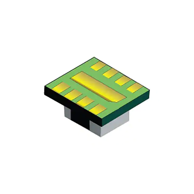
2.8-mm x 3.0-mm x 1.3-mm 8-Pin µSiL package
To maximize efficiency, the converter operates in
PWM mode with a nominal switching frequency of
2.4MHz and automatically enters Power Save Mode
operation at light load currents. In Power Save Mode,
the device operates with typically 17-µA quiescent
current. Using the DCS-Control topology, the device
achieves excellent load transient performance and
accurate output voltage regulation. The EN and PG
pins, which support sequencing configurations, bring
a flexible system design. An integrated soft startup
reduces the inrush current required from the input
supply. Over temperature protection and Hiccup short
circuit protection deliver a robust and reliable solution.
Device Information (1)
2 Applications
•
•
•
•
•
•
PART NUMBER
Optical module
Single board computer
Solid state drive
Metro data center
Audio/video control system
Radar
PACKAGE
BODY SIZE (NOM)
TPS82085
µSiL (8)
2.8 mm x 3.0 mm
TPS82084
µSiL (8)
2.8 mm x 3.0 mm
Device Comparison
(1)
PART NUMBER
OUTPUT CURRENT
TPS82084
2A
TPS82085
3A
For all available packages, see the orderable addendum at
the end of the datasheet.
space
1.8 V Output Application
1.8 V Output Efficiency
TPS82085
VIN
2.5V to 6V C1
10µF
VIN
VOUT
R1
200k
EN
R3
499k
C2
22µF
VOUT
1.8V/3A
100
FB
PG
90
R2
160k
POWER GOOD
Efficiency (%)
GND
80
70
60
1m
VIN = 3.0 V
VIN = 3.5 V
VIN = 4.0 V
VIN = 5.0 V
10m
100m
Load (A)
1
5
D002
1
An IMPORTANT NOTICE at the end of this data sheet addresses availability, warranty, changes, use in safety-critical applications,
intellectual property matters and other important disclaimers. PRODUCTION DATA.
�TPS82085, TPS82084
SLVSCN4D – OCTOBER 2014 – REVISED JUNE 2019
www.ti.com
Table of Contents
1
2
3
4
5
6
7
Features ..................................................................
Applications ...........................................................
Description .............................................................
Revision History.....................................................
Pin Configuration and Functions .........................
Specifications.........................................................
1
1
1
2
3
3
6.1
6.2
6.3
6.4
6.5
6.6
3
3
3
4
4
6
Absolute Maximum Ratings ......................................
ESD Ratings..............................................................
Recommend Operating Conditions...........................
Thermal Information ..................................................
Electrical Characteristics..........................................
Typical Characteristics ..............................................
Detailed Description .............................................. 7
7.1
7.2
7.3
7.4
Overview ...................................................................
Functional Block Diagram .........................................
Feature Description...................................................
Device Functional Modes..........................................
7
7
7
9
8
Application and Implementation ........................ 10
8.1 Application Information............................................ 10
8.2 Typical Applications ................................................ 10
9 Power Supply Recommendations...................... 16
10 Layout................................................................... 16
10.1 Layout Guidelines ................................................. 16
10.2 Layout Example .................................................... 16
10.3 Thermal Consideration.......................................... 16
11 Device and Documentation Support ................. 17
11.1
11.2
11.3
11.4
11.5
11.6
Device Support......................................................
Related Links ........................................................
Community Resources..........................................
Trademarks ...........................................................
Electrostatic Discharge Caution ............................
Glossary ................................................................
17
17
17
17
17
17
12 Mechanical, Packaging, and Orderable
Information ........................................................... 17
12.1 Tape and Reel Information ................................... 18
4 Revision History
Changes from Revision C (September 2018) to Revision D
Page
•
Correct the part number in the title ........................................................................................................................................ 1
•
Add the input voltage range for the output voltage discharge feature in Enable and Disable. ............................................. 9
Changes from Revision B (April 2015) to Revision C
Page
•
Added TPS82084 device into this data sheet ....................................................................................................................... 1
•
Changed from –40 ºC to –55 ºC for storage temperature range ........................................................................................... 3
•
Added thermal information for TPS82085EVM-672. Updated thermal metric value. ............................................................ 4
•
Added power save mode waveform diagram to Power Save Mode (PSM) .......................................................................... 8
•
Added typical value of the EN pin high/low level input voltage in Enable and Disable.......................................................... 9
•
Added pg pin logic table in Power Good Output ................................................................................................................... 9
•
Added integrated inductor information in Application Information ....................................................................................... 10
•
Added additional efficiency curves and a reference hyperlink to the BOM, Table 3 ........................................................... 12
•
Added radiated emission performance graph ..................................................................................................................... 14
Changes from Revision A (April 2015) to Revision B
•
Page
Changed the ESD Ratings Charged device model (CDM) From: ±500 V To: ±1000 V......................................................... 3
Changes from Original (October 2014) to Revision A
•
2
Page
Changed the data sheet From: 3-page Product Preview To: Production data ..................................................................... 1
Submit Documentation Feedback
Copyright © 2014–2019, Texas Instruments Incorporated
Product Folder Links: TPS82085 TPS82084
�TPS82085, TPS82084
www.ti.com
SLVSCN4D – OCTOBER 2014 – REVISED JUNE 2019
5 Pin Configuration and Functions
µSiL Package
(Top View)
1
PG
2
VIN
3
VIN
4
E
TH XPOS
ER
MA ED
LP
AD
EN
8
VOUT
7
FB
6
GND
5
GND
Pin Functions
PIN
NAME
I/O
NO.
DESCRIPTION
EN
1
I
Enable pin. Pull High to enable the device. Pull Low to disable the device. This pin has an
internal pull-down resistor of typically 400 kΩ when the device is disabled.
PG
2
O
Power good open drain output pin. A pull-up resistor can be connected to any voltage less
than 6V. Leave it open if it is not used.
VIN
3,4
PWR
GND
5,6
Input voltage pin.
Ground pin.
Feedback reference pin. An external resistor divider connected to this pin programs the
output voltage.
FB
7
I
VOUT
8
PWR
Exposed
Thermal Pad
Output voltage pin.
The exposed thermal pad must be connected to the GND pin. Must be soldered to achieve
appropriate power dissipation and mechanical reliability.
6 Specifications
6.1 Absolute Maximum Ratings (1)
MIN
Voltage at pins
(2)
Sink current
EN, PG, VIN, FB, VOUT
-0.3
PG
MAX
UNIT
7
V
1.0
mA
Module operating temperature range
-40
125
°C
Storage temperature range
–55
125
°C
(1)
(2)
Stresses beyond those listed under absolute maximum ratings may cause permanent damage to the device. These are stress ratings
only, and functional operation of the device at these or any other conditions beyond those indicated under recommended operating
conditions is not implied. Exposure to absolute-maximum-rated conditions for extended periods may affect device reliability.
All voltage values are with respect to network ground pin.
6.2 ESD Ratings
VALUE
Human body model (HBM), per ANSI/ESDA/JEDEC JS-001
V(ESD)
(1)
(2)
Electrostatic discharge
(1)
UNIT
±2000
Charged device model (CDM), per JEDEC specification JESD22C101 (2)
V
±1000
JEDEC document JEP155 states that 500-V HBM allows safe manufacturing with a standard ESD control process.
JEDEC document JEP157 states that 250-V CDM allows safe manufacturing with a standard ESD control process.
6.3 Recommend Operating Conditions
Over operating free-air temperature range, unless otherwise noted.
VIN
Input voltage range
VPG
Power good pull-up resistor voltage
Copyright © 2014–2019, Texas Instruments Incorporated
Product Folder Links: TPS82085 TPS82084
MIN
MAX
UNIT
2.5
6
V
6
V
Submit Documentation Feedback
3
�TPS82085, TPS82084
SLVSCN4D – OCTOBER 2014 – REVISED JUNE 2019
www.ti.com
Recommend Operating Conditions (continued)
Over operating free-air temperature range, unless otherwise noted.
VOUT
Output voltage range
IOUT
TJ
(1)
MIN
MAX
UNIT
0.8
VIN
V
Output current range, TPS82084 (1)
0
2
A
Output current range, TPS82085 (1)
0
3
A
-40
125
°C
Module operating temperature range
(1)
The module operating temperature range includes module self temperature rise and IC junction temperature rise. In applications where
high power dissipation is present, the maximum operating temperature or maximum output current must be derated.
6.4 Thermal Information
THERMAL METRIC (1)
TPS82084/5SIL
(JEDEC 51-5)
TPS82085EVM-672
RθJA
Junction-to-ambient thermal resistance
64.6
46.6
RθJC(top)
Junction-to-case (top) thermal resistance
30.1
n/a (2)
RθJB
Junction-to-board thermal resistance
23.5
n/a (2)
ψJT
Junction-to-top characterization parameter
0.1
0.1
ψJB
Junction-to-board characterization parameter
23.3
24.6
RθJC(bot)
Junction-to-case (bottom) thermal resistance
17.2
15.4
(1)
(2)
UNIT
°C/W
For more information about traditional and new thermal metrics, see the IC Package Thermal Metrics application report, SPRA953
Not applicable to an EVM
6.5
Electrical Characteristics
TJ = -40°C to 125°C and VIN = 2.5V to 6V. Typical values are at TJ = 25°C and VIN = 3.6V, unless otherwise noted.
PARAMETER
TEST CONDITIONS
MIN
TYP
MAX
UNIT
SUPPLY
VIN
Input voltage range
2.5
IQ
Quiescent current into VIN
No load, device not switching
TJ = -40°C to 85°C, VIN = 2.5 V to 5.5 V
ISD
Shutdown current into VIN
EN = Low,
TJ = -40°C to 85°C, VIN = 2.5 V to 5.5 V
VUVLO
Under voltage lock out threshold
TJSD
6
V
17
25
µA
0.7
5
µA
VIN falling
2.1
2.2
2.3
V
VIN rising
2.3
2.4
2.5
V
Thermal shutdown threshold
TJ rising
150
°C
Thermal shutdown hysteresis
TJ falling
20
°C
LOGIC INTERFACE EN
VIH
High-level input voltage
VIL
Low-level input voltage
1.0
V
Ilkg(EN)
Input leakage current into EN pin
EN = High
0.01
RPD
Pull-down resistance at EN pin
EN = Low
400
0.4
V
0.16
µA
kΩ
SOFT START, POWER GOOD
tSS
Soft start time
Time from EN high to 95% of VOUT nominal
95%
98%
VOUT falling, referenced to VOUT nominal
88%
90%
93%
0.4
V
0.01
0.16
µA
Power good threshold
VPG,OL
Low-level output voltage
Isink = 1mA
Ilkg(PG)
Input leakage current into PG pin
VPG = 5V
Submit Documentation Feedback
ms
93%
VPG
4
0.8
VOUT rising, referenced to VOUT nominal
Copyright © 2014–2019, Texas Instruments Incorporated
Product Folder Links: TPS82085 TPS82084
�TPS82085, TPS82084
www.ti.com
SLVSCN4D – OCTOBER 2014 – REVISED JUNE 2019
Electrical Characteristics (continued)
TJ = -40°C to 125°C and VIN = 2.5V to 6V. Typical values are at TJ = 25°C and VIN = 3.6V, unless otherwise noted.
PARAMETER
TEST CONDITIONS
MIN
TYP
MAX
UNIT
OUTPUT
VOUT
Output voltage range
0.8
VIN
PWM mode
792
800
808
PSM mode, COUT = 22 µF
792
800
817
0.1
V
VFB
Feedback regulation voltage
mV
Ilkg(FB)
Feedback input leakage current
VFB = 0.8 V
0.01
RDIS
Output discharge resistor
EN = Low, VOUT = 1.8 V
260
Ω
Line regulation
IOUT = 1 A, VIN = 2.5 V to 6 V
0.02
%/V
Load regulation
IOUT = 0.5 A to 3 A
0.16
%/A
µA
POWER SWITCH
RDS(on)
RDP
High-side FET on-resistance
ISW = 500 mA
31
56
mΩ
Low-side FET on-resistance
ISW = 500 mA
23
45
mΩ
Dropout resistance
100% mode
69
ILIMF
High-side FET switch current limit
fSW
PWM switching frequency
TPS82085
3.7
4.6
TPS82084
3.6
IOUT = 1 A
2.4
Copyright © 2014–2019, Texas Instruments Incorporated
Product Folder Links: TPS82085 TPS82084
mΩ
5.5
Submit Documentation Feedback
A
MHz
5
�TPS82085, TPS82084
SLVSCN4D – OCTOBER 2014 – REVISED JUNE 2019
www.ti.com
25
0.08
20
$
0.10
4XLHVFHQW &XUUHQW
Dropout Resistance (:)
6.6 Typical Characteristics
0.06
0.04
0.02
0.00
2.5
3.5
10
5
TJ = -40°C
TJ = 25°C
TJ = 85°C
3.0
15
4.0
4.5
Input Voltage (V)
5.0
5.5
6.0
TJ = -40°C
TJ = 25°C
TJ = 85°C
0
2.5
3.0
3.5
D017
Figure 1. Dropout Resistance
4.0
4.5
Input Voltage (V)
5.0
5.5
6.0
D020
Figure 2. Quiescent Current
2.5
6KXWGRZQ &XUUHQW
$
2.0
TJ = -40°C
TJ = 25°C
TJ = 85°C
1.5
1.0
0.5
0.0
2.5
3.0
3.5
4.0
4.5
Input Voltage (V)
5.0
5.5
6.0
D021
Figure 3. Shutdown Current
6
Submit Documentation Feedback
Copyright © 2014–2019, Texas Instruments Incorporated
Product Folder Links: TPS82085 TPS82084
�TPS82085, TPS82084
www.ti.com
SLVSCN4D – OCTOBER 2014 – REVISED JUNE 2019
7 Detailed Description
7.1 Overview
The TPS82084/5 synchronous step-down converter power modules are based on DCS-Control™ (Direct Control
with Seamless transition into Power Save Mode). This is an advanced regulation topology that combines the
advantages of hysteretic, voltage and current mode control.
The DCS-Control™ topology operates in PWM (Pulse Width Modulation) mode for medium to heavy load
conditions and in PSM (Power Save Mode) at light load currents. In PWM, the converter operates with its
nominal switching frequency of 2.4 MHz having a controlled frequency variation over the input voltage range. As
the load current decreases, the converter enters Power Save Mode, reducing the switching frequency and
minimizing the IC's quiescent current to achieve high efficiency over the entire load current range. DCS-Control™
supports both operation modes using a single building block and therefore has a seamless transition from PWM
to PSM without effects on the output voltage. The device offers excellent DC voltage regulation and load
transient regulation, combined with low output voltage ripple, minimizing interference with RF circuits.
7.2 Functional Block Diagram
PG
Hiccup
Counter
VFB
VREF
EN
400kΩ
(1)
VIN
High Side
Current Sense
Bandgap
Undervoltage Lockout
Thermal Shutdown
L
(2)
MOSFET Driver
Control Logic
Ramp
Direct Control
and
Compensation
Comparator
Timer
ton
VOUT
FB
Error Amplifier
DCS - Control
TM
EN
VREF
Output Discharge
Logic
260Ω
GND
Note:
(1) When the device is enabled, the 400 kΩ resistor is disconnected.
(2) The integrated inductor in the module, L = 0.47µH.
7.3 Feature Description
7.3.1 Power Save Mode (PSM)
The device includes a fixed on-time (tON) circuitry. This tON, in steady-state operation in PWM and PSM modes, is
estimated as:
t ON = 420 ns ´
V OUT
V IN
2 ´ I OUT
f PSM =
t ON2 ´
V IN
V OUT
´
V IN - V OUT
L
(1)
To maintain high efficiency at light loads, the device enters Power Save Mode seamlessly when the load current
decreases. This happens when the load current becomes smaller than half the inductor's ripple current. In PSM,
the converter operates with a reduced switching frequency and with a minimum quiescent current to maintain
high efficiency. The on time in PSM is also based on the same tON circuitry. The switching frequency in PSM is
shown in Equation 1.
Copyright © 2014–2019, Texas Instruments Incorporated
Product Folder Links: TPS82085 TPS82084
Submit Documentation Feedback
7
�TPS82085, TPS82084
SLVSCN4D – OCTOBER 2014 – REVISED JUNE 2019
www.ti.com
Feature Description (continued)
In PSM, the output voltage rises slightly above the nominal output voltage in PWM mode. This effect is reduced
by increasing the output capacitance. The output voltage accuracy in PSM operation is reflected in the electrical
specification table and given for a 22-µF output capacitor.
During PAUSE period in PSM (shown in Figure 4), the device does not change the PG pin state nor does it
detect an UVLO event, in order to achieve a minimum quiescent current and maintain high efficiency at light
loads.
VOUT
tPAUSE
IINDUCTOR
tON
Figure 4. Power Save Mode Waveform Diagram
7.3.2 Low Dropout Operation (100% Duty Cycle)
The device offers a low input to output voltage differential by entering 100% duty cycle mode. In this mode, the
high-side MOSFET switch is constantly turned on. This is particularly useful in battery powered applications to
achieve longest operation time by taking full advantage of the whole battery voltage range. The minimum input
voltage to maintain a minimum output voltage is given by:
VIN(min) = VOUT(min) + IOUT x RDP
(2)
Where
RDP = Resistance from VIN to VOUT, including high-side FET on-resistance and DC resistance of the inductor.
VOUT(min) = Minimum output voltage the load can accept.
7.3.3 Soft Startup
The device has an internal soft start circuit which ramps up the output voltage to the nominal voltage during a
soft start time of typically 0.8ms. This avoids excessive inrush current and creates a smooth output voltage slope.
It also prevents excessive voltage drops of primary cells and rechargeable batteries with high internal
impedance. The device is able to monotonically start into a pre-biased output capacitor. The device starts with
the applied bias voltage and ramps the output voltage to its nominal value.
7.3.4 Switch Current Limit and Short Circuit Protection (Hiccup-Mode)
The switch current limit prevents the device from high inductor current and from drawing excessive current from
the battery or input voltage rail. Excessive current might occur with a heavy load/shorted output circuit condition.
If the inductor peak current reaches the switch current limit, the high-side FET is turned off and the low-side FET
is turned on to ramp down the inductor current. Once this switch current limits is triggered 32 times, the devices
stop switching and enables the output discharge. The devices then automatically start a new startup after a
typical delay time of 66μs has passed. This is named HICCUP short circuit protection. The devices repeat this
mode until the high load condition disappears.
7.3.5 Undervoltage Lockout
To avoid mis-operation of the device at low input voltages, an under voltage lockout is implemented, which shuts
down the devices at voltages lower than VUVLO with a hysteresis of 200 mV.
7.3.6 Thermal Shutdown
The device goes into thermal shutdown and stops switching once the junction temperature exceeds TJSD. Once
the device temperature falls below the threshold by 20°C, the device returns to normal operation automatically.
8
Submit Documentation Feedback
Copyright © 2014–2019, Texas Instruments Incorporated
Product Folder Links: TPS82085 TPS82084
�TPS82085, TPS82084
www.ti.com
SLVSCN4D – OCTOBER 2014 – REVISED JUNE 2019
7.4 Device Functional Modes
7.4.1 Enable and Disable
The device is enabled by setting the EN pin to a logic High (typical 0.8 V). Accordingly, shutdown mode is forced
if the EN pin is pulled Low (typical 0.7 V) with a shutdown current of typically 0.7 μA. An internal resistor of 260 Ω
discharges the output via the VOUT pin smoothly when the device is disabled. The output discharge function
also works when thermal shutdown, undervoltage lockout or short circuit protection are triggered. The output
discharge function stops working when the input voltage has decreased to around 0.5V.
An internal pull-down resistor of 400 kΩ is connected to the EN pin when the EN pin is Low. The pull-down
resistor is disconnected when the EN pin is High.
7.4.2 Power Good Output
The device has a power good (PG) output. The PG pin goes high impedance once the output is above 95% of
the nominal voltage, and is driven low once the output voltage falls below typically 90% of the nominal voltage.
The PG pin is an open drain output and is specified to sink up to 1 mA. The power good output requires a pull-up
resistor connecting to any voltage rail less than 6 V.
The PG signal can be used for sequencing of multiple rails by connecting it to the EN pin of other converters.
Leave the PG pin floating when it is not used. Table 1 shows the PG pin logic.
Table 1. PG Pin Logic
DEVICE CONDITIONS
Enable
EN = High, VFB ≥ VPG
LOGIC STATUS
HIGH Z
LOW
√
EN = High, VFB < VPG
√
Shutdown
EN = Low
√
Thermal Shutdown
TJ > TJSD
√
UVLO
0.5 V < VIN < VUVLO
Power Supply Removal
VIN ≤ 0.5 V
√
√
Copyright © 2014–2019, Texas Instruments Incorporated
Product Folder Links: TPS82085 TPS82084
Submit Documentation Feedback
9
�TPS82085, TPS82084
SLVSCN4D – OCTOBER 2014 – REVISED JUNE 2019
www.ti.com
8 Application and Implementation
NOTE
Information in the following applications sections is not part of the TI component
specification, and TI does not warrant its accuracy or completeness. TI’s customers are
responsible for determining suitability of components for their purposes. Customers should
validate and test their design implementation to confirm system functionality.
8.1 Application Information
The TPS82084/5 are synchronous step-down converter power modules whose output voltage is adjusted by
component selection. The following section discusses the design of the external components to complete the
power supply design for several input and output voltage options by using typical applications as a reference.
The required power inductor is integrated inside the TPS82084/5. The inductor is shielded and has an
inductance of 0.47 µH with approximately a +/- 20% tolerance. The TPS82084 and TPS82085 are pin-to-pin and
BOM-to-BOM compatible, differing only in their rated output current.
8.2 Typical Applications
8.2.1
1.2-V Output Application
TPS82085
VIN
2.5V to 6V C1
10µF
VIN
VOUT
R1
80.6k
EN
C2
22µF
R3
499k
VOUT
1.2V/3A
FB
GND
PG
R2
162k
POWER GOOD
Figure 5. 1.2-V Output Application
8.2.1.1 Design Requirements
For this design example, use the input parameters shown in Table 2.
Table 2. Design Parameters
DESIGN PARAMETER
EXAMPLE VALUE
Input voltage range
2.5 V to 6 V
Output voltage
1.2 V
Output ripple voltage
< 20 mV
Output current rating
3A
Table 3 lists the components used for the example.
Table 3. List of Components
REFERENCE
10
DESCRIPTION
MANUFACTURER
C1
10µF, Ceramic Capacitor, 10V, X7R, size 0805, GRM21BR71A106KE51
C2
22µF, Ceramic Capacitor, 6.3V, X7R, size 0805, CL21B226MQQNNNE
or
22µF, Ceramic Capacitor, 6.3V, X7S, size 0805, C2012X7S1A226M125AC
R1
Depending on the output voltage, 1% accuracy
Std
R2
162kΩ, 1% accuracy
Std
R3
499kΩ, 1% accuracy
Std
Submit Documentation Feedback
Murata
Samsung
or
TDK
Copyright © 2014–2019, Texas Instruments Incorporated
Product Folder Links: TPS82085 TPS82084
�TPS82085, TPS82084
www.ti.com
SLVSCN4D – OCTOBER 2014 – REVISED JUNE 2019
8.2.1.2 Detailed Design Procedure
8.2.1.2.1 Setting the Output Voltage
The output voltage is set by an external resistor divider according to the following equations:
R1 ö
R1 ö
æ
æ
VOUT = VFB ´ ç 1 +
= 0.8 V ´ ç 1 +
÷
R2 ø
R2 ÷ø
è
è
(3)
R2 should not be higher than 180 kΩ to achieve high efficiency at light load while providing acceptable noise
sensitivity. Larger currents through R2 improve noise sensitivity and output voltage accuracy. Figure 5 shows a
recommended external resistor divider value for a 1.2-V output. Choose appropriate resistor values for other
output voltages.
8.2.1.2.2
Input and Output Capacitor Selection
For best output and input voltage filtering, ceramic capacitors are required. The input capacitor minimizes input
voltage ripple, suppresses input voltage spikes and provides a stable system rail for the device. A 10-µF or larger
input capacitor is required. The output capacitor value can range from 22 µF up to more than 150 µF. The
recommended typical output capacitor value is 22µF. Values over 150 µF may be possible with a reduced load
during startup in order to avoid triggering the Hiccup short circuit protection. A feed forward capacitor is not
required for proper operation.
Ceramic capacitor has a DC-Bias effect, which has a strong influence on the final effective capacitance. Choose
the right capacitor carefully in combination with considering its package size and voltage rating. Ensure that the
input effective capacitance is at least 5µF and the output effective capacitance is at least 8µF.
Copyright © 2014–2019, Texas Instruments Incorporated
Product Folder Links: TPS82085 TPS82084
Submit Documentation Feedback
11
�TPS82085, TPS82084
SLVSCN4D – OCTOBER 2014 – REVISED JUNE 2019
www.ti.com
8.2.1.3 Application Performance Curves
100
100
90
90
Efficiency (%)
Efficiency (%)
TA = 25°C, VIN = 5 V, VOUT = 1.2 V, BOM = Table 3 unless otherwise noted.
80
70
70
VIN = 3.0 V
VIN = 3.5 V
VIN = 4.0 V
VIN = 5.0 V
60
1m
10m
80
100m
Load (A)
1
VIN = 3.0 V, TA = 25 °C
VIN = 3.0 V, TA = 85 °C
VIN = 5.0 V, TA = 25 °C
VIN = 5.0 V, TA = 85 °C
60
1m
5
10m
D001
VOUT = 1.2 V
90
90
Efficiency (%)
Efficiency (%)
100
80
70
VIN = 3.0 V
VIN = 3.5 V
VIN = 4.0 V
VIN = 5.0 V
10m
100m
Load (A)
1
VIN = 3.0 V, TA = 25 °C
VIN = 3.0 V, TA = 85 °C
VIN = 5.0 V, TA = 25 °C
VIN = 5.0 V, TA = 85 °C
60
1m
5
10m
D002
100
90
90
Efficiency (%)
Efficiency (%)
1
5
D023
Figure 9. Efficiency
100
80
10m
80
70
VIN = 3.0 V
VIN = 3.5 V
VIN = 4.0 V
VIN = 5.0 V
100m
Load (A)
1
5
D003
VOUT = 2.6 V
VIN = 3.0 V, TA = 25 °C
VIN = 3.0 V, TA = 85 °C
VIN = 5.0 V, TA = 25 °C
VIN = 5.0 V, TA = 85 °C
60
1m
10m
Submit Documentation Feedback
100m
Load (A)
1
5
D024
VOUT = 2.6 V
Figure 11. Efficiency
Figure 10. Efficiency
12
100m
Load (A)
VOUT = 1.8 V
Figure 8. Efficiency
60
1m
D022
80
VOUT = 1.8 V
70
5
Figure 7. Efficiency
100
60
1m
1
VOUT = 1.2 V
Figure 6. Efficiency
70
100m
Load (A)
Copyright © 2014–2019, Texas Instruments Incorporated
Product Folder Links: TPS82085 TPS82084
�TPS82085, TPS82084
www.ti.com
SLVSCN4D – OCTOBER 2014 – REVISED JUNE 2019
100
100
90
90
Efficiency (%)
Efficiency (%)
TA = 25°C, VIN = 5 V, VOUT = 1.2 V, BOM = Table 3 unless otherwise noted.
80
70
80
70
VIN = 3.5 V
VIN = 4.0 V
VIN = 5.0 V
60
1m
10m
VIN = 5.0 V, TA = 25 °C
VIN = 5.0 V, TA = 85 °C
100m
Load (A)
1
60
1m
5
10m
VOUT = 3.3 V
4
4
3
3
Output Current (A)
Output Current (A)
5
D025
Figure 13. Efficiency
2
2
1
1
VIN = 3.0 V
VIN = 3.5 V
VIN = 5.0 V
VIN = 3.0 V
VIN = 3.5 V
VIN = 5.0 V
0
65
75
85
95
105
Ambient Temperature (°C)
VOUT = 1.2 V
115
0
65
125
75
D018
θJA = 46.6°C/W
85
95
105
Ambient Temperature (°C)
VOUT = 2.6 V
115
125
D019
θJA = 46.6°C/W
Figure 14. Thermal Derating
Figure 15. Thermal Derating
1.0
1.0
Output Voltage Accuracy (%)
Output Voltage Accuracy (%)
1
VOUT = 3.3 V
Figure 12. Efficiency
0.5
0.0
-0.5
TA = -40°C
TA = 25°C
TA = 85°C
-1.0
1m
100m
Load (A)
D004
10m
100m
Load (A)
1
5
0.5
0.0
-0.5
TA = -40°C
TA = 25°C
TA = 85°C
-1.0
2.5
3.0
D005
3.5
4.0
4.5
Input Voltage (V)
5.0
5.5
6.0
D006
IOUT = 1 A
Figure 16. Load Regulation
Copyright © 2014–2019, Texas Instruments Incorporated
Product Folder Links: TPS82085 TPS82084
Figure 17. Line Regulation
Submit Documentation Feedback
13
�TPS82085, TPS82084
SLVSCN4D – OCTOBER 2014 – REVISED JUNE 2019
www.ti.com
TA = 25°C, VIN = 5 V, VOUT = 1.2 V, BOM = Table 3 unless otherwise noted.
VIN
50mV/DIV
AC
VIN
20mV/DIV
AC
VOUT
10mV/DIV
AC
VOUT
10mV/DIV
AC
7LPH
Time - 250ns/DIV
V ',9
D007
IOUT = 2 A
D008
IOUT = 25 mA
Figure 18. Input and Output Ripple in PWM Mode
Figure 19. Input and Output Ripple in PSM Mode
IOUT
2A/DIV
IOUT
1A/DIV
VOUT
50mV/DIV
AC
VOUT
10mV/DIV
AC
7LPH
Time - 10ms/DIV
V ',9
D010
D009
IOUT = 25 mA to 3 A
IOUT = 25 mA to 3 A
Figure 20. Load Sweep
Figure 21. Load Transient
EN
2V/DIV
IOUT
2A/DIV
VOUT
500mV/DIV
VOUT
20mV/DIV
AC
IOUT
2A/DIV
7LPH
V ',9
Time - 2ms/DIV
D011
IOUT = 0.5 A to 2.5 A
Figure 22. Load Transient
14
D012
IOUT = no load
Submit Documentation Feedback
Figure 23. Startup / Shutdown without Load
Copyright © 2014–2019, Texas Instruments Incorporated
Product Folder Links: TPS82085 TPS82084
�TPS82085, TPS82084
www.ti.com
SLVSCN4D – OCTOBER 2014 – REVISED JUNE 2019
TA = 25°C, VIN = 5 V, VOUT = 1.2 V, BOM = Table 3 unless otherwise noted.
EN
2V/DIV
VOUT
600mV/DIV
VOUT
500mV/DIV
IOUT
2A/DIV
IOUT
2.5A/DIV
7LPH
V ',9
7LPH
V ',9
D013
Load = 0.4 Ω
D014
IOUT = 3 A
Figure 24. Startup / Shutdown with Resistive Load
Figure 25. Short Circuit, HICCUP Protection Entry / Exit
0.004
IOUT = 100 mA
IOUT = 2.5 A
80
Spurious Output Noise (V)
Power Supply Rejection Ratio (dB)
100
60
40
20
0.003
0.002
0.001
IOUT = 100 mA
IOUT = 2.5 A
0
100
0
1k
10k
Frequency (Hz)
100k
1M
2M
D015
Figure 26. Power Supply Rejection Ratio (PSRR)
60
D016
Horizontal - QPK
Vertical - QPK
CISPR11 Group 1 Class B 3m QP
50
/HYHO G% 9 P
/HYHO G% 9 P
10M
70
Horizontal - QPK
Vertical - QPK
CISPR11 Group 1 Class B 3m QP
50
40
30
40
30
20
20
10
10
0
30
8M
Figure 27. Spurious Output Noise
70
60
4M
6M
Frequency (Hz)
40 50 6070
100
200
300 400500 700 1000
Frequency (MHz)
D026
RLOAD = 0.47 Ω, VIN = 5 V (battery supply), VOUT = 1.2 V, EMI
test board without filters
Figure 28. TPS82085 Radiated Emission
0
30
40 50 6070
100
200
300 400500 700 1000
Frequency (MHz)
D027
RLOAD = 0.68 Ω, VIN = 5 V (battery supply), VOUT = 1.2 V, EMI
test board without filters
Figure 29. TPS82084 Radiated Emission
Copyright © 2014–2019, Texas Instruments Incorporated
Product Folder Links: TPS82085 TPS82084
Submit Documentation Feedback
15
�TPS82085, TPS82084
SLVSCN4D – OCTOBER 2014 – REVISED JUNE 2019
www.ti.com
9 Power Supply Recommendations
The devices are designed to operate from an input supply voltage range between 2.5 V and 6 V. The average
input current of the TPS82084/5 is calculated as:
´I
1 V
IIN = ´ OUT OUT
h
VIN
(4)
Ensure that the power supply has a sufficient current rating for the application.
10 Layout
10.1 Layout Guidelines
•
•
•
•
•
It is recommended to place all components as close as possible to the IC. Specially, the input capacitor
placement must be closest to the VIN and GND pins of the device.
Use wide and short traces for the main current paths to reduce the parasitic inductance and resistance.
To enhance heat dissipation of the device, the exposed thermal pad should be connected to bottom or
internal layer ground planes using vias.
Refer to Figure 30 for an example of component placement, routing and thermal design.
The recommended land pattern for the TPS82084/5 is shown at the end of this data sheet. For best
manufacturing results, it is important to create the pads as solder mask defined (SMD). This keeps each pad
the same size and avoids solder pulling the device during reflow.
10.2 Layout Example
R2
R1
VOUT
EN
VIN
VOUT
PG
FB
VIN
GND
VIN
GND
Total Solution Size
2
35 mm
C1
C2
GND
Figure 30. TPS82084/5 PCB Layout
10.3 Thermal Consideration
The TPS82084/5's output current needs to be derated when the device operates in a high ambient temperature
or deliver high output power. The amount of current derated is dependent upon the input voltage, output power,
PCB layout design and environmental thermal condition.
The TPS82084/5 module temperature must be kept less than the maximum rating of 125°C. Three basic
approaches for enhancing thermal performance are listed below:
• Improve the power dissipation capability of the PCB design.
• Improve the thermal coupling of the component to the PCB.
• Introduce airflow into the system.
To estimate approximate module temperature of TPS82084/5, apply the typical efficiency stated in this datasheet
to the desired application condition for the module power dissipation, then calculate the module temperature rise
by multiplying the power dissipation by its thermal resistance. For more details on how to use the thermal
parameters in real applications, see the application notes: SZZA017 and SPRA953.
16
Submit Documentation Feedback
Copyright © 2014–2019, Texas Instruments Incorporated
Product Folder Links: TPS82085 TPS82084
�TPS82085, TPS82084
www.ti.com
SLVSCN4D – OCTOBER 2014 – REVISED JUNE 2019
11 Device and Documentation Support
11.1 Device Support
11.1.1 Third-Party Products Disclaimer
TI'S PUBLICATION OF INFORMATION REGARDING THIRD-PARTY PRODUCTS OR SERVICES DOES NOT
CONSTITUTE AN ENDORSEMENT REGARDING THE SUITABILITY OF SUCH PRODUCTS OR SERVICES
OR A WARRANTY, REPRESENTATION OR ENDORSEMENT OF SUCH PRODUCTS OR SERVICES, EITHER
ALONE OR IN COMBINATION WITH ANY TI PRODUCT OR SERVICE.
11.2 Related Links
The table below lists quick access links. Categories include technical documents, support and community
resources, tools and software, and quick access to order now.
Table 4. Related Links
PARTS
PRODUCT FOLDER
ORDER NOW
TECHNICAL
DOCUMENTS
TOOLS &
SOFTWARE
SUPPORT &
COMMUNITY
TPS82085
Click here
Click here
Click here
Click here
Click here
TPS82084
Click here
Click here
Click here
Click here
Click here
11.3 Community Resources
The following links connect to TI community resources. Linked contents are provided "AS IS" by the respective
contributors. They do not constitute TI specifications and do not necessarily reflect TI's views; see TI's Terms of
Use.
TI E2E™ Online Community TI's Engineer-to-Engineer (E2E) Community. Created to foster collaboration
among engineers. At e2e.ti.com, you can ask questions, share knowledge, explore ideas and help
solve problems with fellow engineers.
Design Support TI's Design Support Quickly find helpful E2E forums along with design support tools and
contact information for technical support.
11.4 Trademarks
MicroSiP, DCS-Control, E2E are trademarks of Texas Instruments.
11.5 Electrostatic Discharge Caution
These devices have limited built-in ESD protection. The leads should be shorted together or the device placed in conductive foam
during storage or handling to prevent electrostatic damage to the MOS gates.
11.6 Glossary
SLYZ022 — TI Glossary.
This glossary lists and explains terms, acronyms, and definitions.
12 Mechanical, Packaging, and Orderable Information
The following pages include mechanical, packaging, and orderable information. This information is the most
current data available for the designated devices. This data is subject to change without notice and revision of
this document. For browser-based versions of this data sheet, refer to the left-hand navigation.
Copyright © 2014–2019, Texas Instruments Incorporated
Product Folder Links: TPS82085 TPS82084
Submit Documentation Feedback
17
�TPS82085, TPS82084
SLVSCN4D – OCTOBER 2014 – REVISED JUNE 2019
www.ti.com
12.1 Tape and Reel Information
REEL DIMENSIONS
TAPE DIMENSIONS
P1
K0
B0 W
Reel
Diameter
Cavity
A0
B0
K0
W
P1
A0
Dimension designed to accommodate the component width
Dimension designed to accommodate the component length
Dimension designed to accommodate the component thickness
Overall width of the carrier tape
Pitch between successive cavity centers
Reel Width (W1)
QUADRANT ASSIGNMENTS FOR PIN 1 ORIENTATION IN TAPE
Sprocket Holes
Q1
Q2
Q1
Q2
Q3
Q4
Q3
Q4
User Direction of Feed
Pocket Quadrants
18
Device
Package
Type
Package
Drawing
Pins
SPQ
Reel
Diameter (mm)
Reel
Width W1 (mm)
A0
(mm)
B0
(mm)
K0
(mm)
P1
(mm)
W
(mm)
Pin1
Quadrant
TPS82084SILR
uSiP
SIL
8
3000
330.0
12.4
3.0
3.2
1.45
4.0
12.0
Q1
TPS82084SILT
uSiP
SIL
8
250
178.0
13.2
3.0
3.2
1.45
4.0
12.0
Q1
TPS82085SILR
uSiP
SIL
8
3000
330.0
12.4
3.0
3.2
1.45
4.0
12.0
Q1
TPS82085SILT
uSiP
SIL
8
250
178.0
13.2
3.0
3.2
1.45
4.0
12.0
Q1
Submit Documentation Feedback
Copyright © 2014–2019, Texas Instruments Incorporated
Product Folder Links: TPS82085 TPS82084
�TPS82085, TPS82084
www.ti.com
SLVSCN4D – OCTOBER 2014 – REVISED JUNE 2019
TAPE AND REEL BOX DIMENSIONS
Width (mm)
W
L
H
Device
Package Type
Package Drawing
Pins
SPQ
Length (mm)
Width (mm)
Height (mm)
TPS82084SILR
uSiP
SIL
8
3000
383
353
58
TPS82084SILT
uSiP
SIL
8
250
223
194
35
TPS82085SILR
uSiP
SIL
8
3000
383
353
58
TPS82085SILT
uSiP
SIL
8
250
223
194
35
Copyright © 2014–2019, Texas Instruments Incorporated
Product Folder Links: TPS82085 TPS82084
Submit Documentation Feedback
19
�TPS82085, TPS82084
SLVSCN4D – OCTOBER 2014 – REVISED JUNE 2019
www.ti.com
PACKAGE OUTLINE
SIL0008C
MicroSiP TM - 1.33 mm max height
SCALE 4.000
MICRO SYSTEM IN PACKAGE
2.9
2.7
B
A
PIN 1 INDEX
AREA
(2.5)
3.1
2.9
PICK AREA
NOTE 3
(2)
1.33 MAX
C
0.08 C
1.1±0.1
EXPOSED
THERMAL PAD
SYMM
(0.05)
TYP
5
4
SYMM
2X
1.9±0.1
1.95
1
8
6X 0.65
8X
0.1
0.05
(45 X0.25)
PIN 1 ID
8X
0.42
0.38
0.52
0.48
C A
C
B
4221448/D 04/2015
MicroSiP is a trademark of Texas Instruments
NOTES:
1. All linear dimensions are in millimeters. Any dimensions in parenthesis are for reference only. Dimensioning and tolerancing
per ASME Y14.5M.
2. This drawing is subject to change without notice.
3. Pick and place nozzle 1.3 mm or smaller recommended.
4. The package thermal pad must be soldered to the printed circuit board for thermal and mechanical performance.
www.ti.com
20
Submit Documentation Feedback
Copyright © 2014–2019, Texas Instruments Incorporated
Product Folder Links: TPS82085 TPS82084
�TPS82085, TPS82084
www.ti.com
SLVSCN4D – OCTOBER 2014 – REVISED JUNE 2019
EXAMPLE BOARD LAYOUT
SIL0008C
MicroSiP TM - 1.33 mm max height
MICRO SYSTEM IN PACKAGE
(1.1)
8X (0.5)
8
1
8X (0.4)
SYMM
(1.9)
(0.75)
6X (0.65)
5
4
SYMM
( 0.2) VIA
TYP
(2.2)
LAND PATTERN EXAMPLE
SOLDER MASK DEFINED
SCALE:20X
0.05 MIN
ALL SIDES
SOLDER MASK
OPENING
METAL UNDER
SOLDER MASK
(R0.05) TYP
DETAIL
NOT TO SCALE
4221448/D 04/2015
NOTES: (continued)
5. This package is designed to be soldered to a thermal pad on the board. For more information, see Texas Instruments literature
number SLUA271 (www.ti.com/lit/slua271).
www.ti.com
Copyright © 2014–2019, Texas Instruments Incorporated
Product Folder Links: TPS82085 TPS82084
Submit Documentation Feedback
21
�TPS82085, TPS82084
SLVSCN4D – OCTOBER 2014 – REVISED JUNE 2019
www.ti.com
EXAMPLE STENCIL DESIGN
SIL0008C
MicroSiP TM - 1.33 mm max height
MICRO SYSTEM IN PACKAGE
(1.04)
SOLDER MASK EDGE
8X (0.5)
(R0.05) TYP
8X (0.4)
(0.85)
METAL
TYP
SYMM
(1.05)
6X (0.65)
SYMM
(2.2)
SOLDER PASTE EXAMPLE
BASED ON 0.125 mm THICK STENCIL
EXPOSED PAD
85% PRINTED SOLDER COVERAGE BY AREA
SCALE:25X
4221448/D 04/2015
NOTES: (continued)
6. Laser cutting apertures with trapezoidal walls and rounded corners may offer better paste release. IPC-7525 may have alternate
design recommendations.
www.ti.com
22
Submit Documentation Feedback
Copyright © 2014–2019, Texas Instruments Incorporated
Product Folder Links: TPS82085 TPS82084
�PACKAGE OPTION ADDENDUM
www.ti.com
17-Feb-2021
PACKAGING INFORMATION
Orderable Device
Status
(1)
Package Type Package Pins Package
Drawing
Qty
Eco Plan
(2)
Lead finish/
Ball material
MSL Peak Temp
Op Temp (°C)
Device Marking
(3)
(4/5)
(6)
TPS82084SILR
ACTIVE
uSiP
SIL
8
3000
RoHS & Green
NIAU
Level-2-260C-1 YEAR
-40 to 125
1D
TPS82084SILT
ACTIVE
uSiP
SIL
8
250
RoHS & Green
Call TI
Level-2-260C-1 YEAR
-40 to 125
1D
TPS82085SILR
ACTIVE
uSiP
SIL
8
3000
RoHS & Green
NIAU
Level-2-260C-1 YEAR
-40 to 125
GE
TPS82085SILT
ACTIVE
uSiP
SIL
8
250
RoHS & Green
NIAU
Level-2-260C-1 YEAR
-40 to 125
GE
(1)
The marketing status values are defined as follows:
ACTIVE: Product device recommended for new designs.
LIFEBUY: TI has announced that the device will be discontinued, and a lifetime-buy period is in effect.
NRND: Not recommended for new designs. Device is in production to support existing customers, but TI does not recommend using this part in a new design.
PREVIEW: Device has been announced but is not in production. Samples may or may not be available.
OBSOLETE: TI has discontinued the production of the device.
(2)
RoHS: TI defines "RoHS" to mean semiconductor products that are compliant with the current EU RoHS requirements for all 10 RoHS substances, including the requirement that RoHS substance
do not exceed 0.1% by weight in homogeneous materials. Where designed to be soldered at high temperatures, "RoHS" products are suitable for use in specified lead-free processes. TI may
reference these types of products as "Pb-Free".
RoHS Exempt: TI defines "RoHS Exempt" to mean products that contain lead but are compliant with EU RoHS pursuant to a specific EU RoHS exemption.
Green: TI defines "Green" to mean the content of Chlorine (Cl) and Bromine (Br) based flame retardants meet JS709B low halogen requirements of


 工商网监
湘ICP备2023018690号
工商网监
湘ICP备2023018690号
