Using the TPS84410EVM-001,
TPS84210EVM-002, TPS84610EVM-003
User's Guide
Literature Number: SLUU633A
September 2011 – Revised February 2012
�User's Guide
SLUU633A – September 2011 – Revised February 2012
TPS84410EVM-001/TPS84210EVM-002/TPS84610EVM-003,
2-A to 6-A Integrated Power Solution
1
Introduction
The TPS84410EVM-001, TPS84210EVM-002, TPS84610EVM-003 Evaluation Module
(TPS84x10EVM-00x) is designed as an easy to use platform that facilitates an extensive evaluation of the
features and performance of the Integrated Power Solution (IPS) devices. The EVM PCB may be
configured with one of three IPS devices (see Table 1).
Table 1. TPS84x10EVM-00x Device Configuration
DEVICE
TITLE
TPS84210
6-V input, 2-A output sync. step-down converter with PWM
TPS84410
6-V input, 4-A output sync. step-down converter with PWM
TPS84610
6-V input, 6-A output sync. step-down converter with PWM
This user guide provides information on the correct usage of the EVM and an explanation of the numerous
test points on the board.
2
Description
The EVM features a TPS84x10 synchronous buck IPS device configured for operation with typical 3.3-V
and 5-V input bus applications. The output voltage can be set to one of five popular values by using a
simple configuration jumper. In similar fashion, the switching frequency can be set to one of four values by
use of a jumper. The full 4-A rated output current can be supplied by the EVM. A minimal amount of input
and output capacitance is used on the board. Component pads are provided for additional input and
output capacitors if desired. Monitoring test points are provided to allow measurement of efficiency, power
dissipation, input ripple, output ripple, line and load regulation, and transient response. Control test points
are provided for use of the PWRGD, Inhibit/UVLO, synchronization, and slow-start/tracking features of the
IPS device. The EVM uses a recommended PCB layout that maximizes thermal performance and
minimizes output ripple and noise.
2
TPS84410EVM-001/TPS84210EVM-002/TPS84610EVM-003, 2-A to 6-A
Integrated Power Solution
SLUU633A – September 2011 – Revised February 2012
Submit Documentation Feedback
Copyright © 2011–2012, Texas Instruments Incorporated
�Getting Started
www.ti.com
3
Getting Started
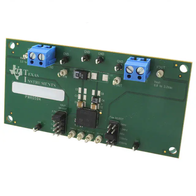
Figure 1 highlights the user interface items associated with the EVM. The polarized VIN Power terminal
block is used for connection to the host input supply and the polarized VOUT Power terminal block is used
for connection to the load. The terminal blocks can except up to 16 AWG wire.
The VIN monitor and VOUT monitor test points located near the power terminal blocks are intended to be
used as voltage monitoring points where voltmeters can be connected to measure VIN and VOUT. The
voltmeter references should be connected to any of the four VIN/VOUT monitor grounds test points located
between the power terminal blocks. Do not use these VIN and VOUT monitoring test points as the input
supply or output load connection points. The PCB traces connecting to these test points are not designed
to support high currents.
Figure 1. TPS84x10EVM-00x User Interface
SLUU633A – September 2011 – Revised February 2012
Submit Documentation Feedback
TPS84410EVM-001/TPS84210EVM-002/TPS84610EVM-003, 2-A to 6-A
Integrated Power Solution
Copyright © 2011–2012, Texas Instruments Incorporated
3
�Getting Started
www.ti.com
The VIN scope and VOUT scope test points can be used to monitor VIN and VOUT waveforms with an
oscilloscope. These test points are intended for use with un-hooded scope probes. The scope probe tip
should be connected to the socket labeled VIN or VOUT, and the scope ground barrel should lean against
to the test point labeled GND. The GND TP may need to be cut or bent slightly to hold the probe barrel.
Metal Ground Barrel
Probe Tip
TP15
TP16
Figure 2. Tip and Barrel Measurement
The control test points located directly below the TPS84x10 IPS device are made available to test the
features of the device. Any external connections made to these test points should be referenced to either
of the two control ground test points located along the bottom of the EVM. Refer to Section 4 of this user
guide for more information on the individual control test points.
The VOUT-select and FSW-select configuration jumpers are provided for selecting the desired output voltage
and appropriate switching frequency. Before applying power to the EVM, ensure that the jumpers are
present and properly positioned for the intended output voltage. Refer to Table 2 for the recommended
jumper settings. Always remove input power before changing the jumper settings.
Once the jumper settings have been confirmed, configure the host input supply to apply the appropriate
bus voltage listed in Table 2 and confirm that the selected output voltage is obtained.
Table 2. Output Voltage and Switching Frequency Jumper Settings
4
VOUT SELECT
TPS84210, FSW
SELECT
TPS84410, FSW
SELECT
TPS84610, FSW
SELECT
VIN BUS VOLTAGE
3.3 V
1.5 MHz
1 MHz
-
5V
2.5 V
1.5 MHz
1 MHz
-
5V
1.8 V
1 MHz
1 MHz
-
5 V or 3.3 V
1.2 V
750 kHz
750 kHz
-
5 V or 3.3 V
0.8 V
650 kHz
650 kHz
-
5 V or 3.3 V
TPS84410EVM-001/TPS84210EVM-002/TPS84610EVM-003, 2-A to 6-A
Integrated Power Solution
SLUU633A – September 2011 – Revised February 2012
Submit Documentation Feedback
Copyright © 2011–2012, Texas Instruments Incorporated
�Test Point Descriptions
www.ti.com
4
Test Point Descriptions
Fourteen wire-loop test points have been provided as convenient connection points for digital voltmeters
(DVM) or oscilloscope probes to aid in the evaluation of the IPS device. A via labled PH is available near
U1 to scope on the switching frequency. A description of each test point is listed in Table 3
Table 3. Test Point Descriptions
TEST POINT
VIN
VOUT
Output voltage monitor. Connect DVM to this point for measuring efficiency, line regulation, and
load regulation.
GND
Input and output voltage monitor grounds (located between terminal blocks). Reference the above
DVMs to any of these four ground points.
VIN (scope)
Input voltage scope monitor. Connect an oscilloscope to this set of points to measure input ripple
voltage.
VOUT (scope)
PWRGD
INH/UVLO
Output voltage scope monitor. Connect an oscilloscope to this set of points to measure output
ripple voltage and transient response.
Monitors the power good signal of the IPS device. This is an open drain signal that requires an
external pull-up resistor to VIN if monitoring is desired. A 10-kΩ to 100-kΩ pull-up resistor is
recommended. PWRGD is high if the output voltage is within 92% to 106% of its nominal value.
Connect this point to control ground to inhibit the IPS device. Allow this point to float to enable the
device. Do not use a pull-up resistor. An external resistor can be connected from this point to
control ground to increase the under-voltage lockout (UVLO) of the device.
RT/CLK
Connects to the RT/CLK pin of the IPS device. An external clock signal can be applied to this
point to synchronize the device to an appropriate frequency.
SS/TR
Connects to the internal slow-start capacitor of the IPS device. An external capacitor can be
connected from this point to control ground to increase the slow-start time of the device. This
point can also be used as an input for tracking applications.
GND
5
DESCRIPTION
Input voltage monitor. Connect DVM to this point for measuring efficiency.
Control grounds (located along bottom of EVM). Reference any signals associated with the
control test points to either of these two ground points.
Operation Notes
The UVLO threshold of the factory-stock EVM is approximately 3.05 V with 0.3 V of hysteresis. The input
voltage must be above the UVLO threshold in order to startup the IPS device. The UVLO threshold can be
increased by adding a resistor to the INH/UVLO test point as described above. After startup, the minimum
input voltage to the IPS device must be at least 2.95 V or (VOUT + 1.1 V), whichever is greater, in order to
produce a regulated output. The maximum operating input voltage for the IPS device is 6 V. Refer to the
TPS84410 datasheet for further information on the input voltage range and UVLO operation.
After application of the proper input voltage, the output voltage of the IPS device will ramp to its final value
in approximately 1 ms. If desired, this soft-start time can be increased by adding a capacitor to the SS/TR
test point as described above. Refer to the TPS84410 datasheet for further information on adjusting the
soft-start time.
Table 1 lists the recommended switching frequencies for each of the VOUT selections. These
recommendations cover operation over a wide range of input voltage and output load conditions. Several
factors such as duty cycle, minimum on-time, minimum off-time, and current limit influence selection of the
appropriate switching frequency. In some applications, other switching frequencies might be used for
particular output voltages, depending on the above factors. Refer to the TPS84410 datasheet for further
information on switching frequency selection, including synchronization.
SLUU633A – September 2011 – Revised February 2012
Submit Documentation Feedback
TPS84410EVM-001/TPS84210EVM-002/TPS84610EVM-003, 2-A to 6-A
Integrated Power Solution
Copyright © 2011–2012, Texas Instruments Incorporated
5
�TPS84x10EVM-00x Schematic
6
www.ti.com
TPS84x10EVM-00x Schematic
Figure 3. TPS84x10EVM-00x Schematic
6
TPS84410EVM-001/TPS84210EVM-002/TPS84610EVM-003, 2-A to 6-A
Integrated Power Solution
SLUU633A – September 2011 – Revised February 2012
Submit Documentation Feedback
Copyright © 2011–2012, Texas Instruments Incorporated
�PCB Layouts
www.ti.com
7
PCB Layouts
Figure 4. Top Layer
Figure 5. Internal 1 Layer
SLUU633A – September 2011 – Revised February 2012
Submit Documentation Feedback
TPS84410EVM-001/TPS84210EVM-002/TPS84610EVM-003, 2-A to 6-A
Integrated Power Solution
Copyright © 2011–2012, Texas Instruments Incorporated
7
�PCB Layouts
www.ti.com
Figure 6. Internal 2 Layer
Figure 7. Bottom Layer
8
TPS84410EVM-001/TPS84210EVM-002/TPS84610EVM-003, 2-A to 6-A
Integrated Power Solution
SLUU633A – September 2011 – Revised February 2012
Submit Documentation Feedback
Copyright © 2011–2012, Texas Instruments Incorporated
�PCB Layouts
www.ti.com
Figure 8. Top Assembly
Figure 9. Bottom Layer
SLUU633A – September 2011 – Revised February 2012
Submit Documentation Feedback
TPS84410EVM-001/TPS84210EVM-002/TPS84610EVM-003, 2-A to 6-A
Integrated Power Solution
Copyright © 2011–2012, Texas Instruments Incorporated
9
�List of Material
8
www.ti.com
List of Material
Table 4. TPS84x10EVM-00x List of Material (1) (2) (3) (4) (5)
(1)
(2)
(3)
(4)
(5)
10
-003
-002
-001
REF DES
DESCRIPTION
Part Number
MFR
1
1
1
C1
Capacitor, ceramic, 10 V, x5R, 10%, 47 µF,
1210
GRM32ER61A476K
Murata
1
1
1
C2
Capacitor, ceramic, 6.3 V, x5R, 20%, 47 µF,
1210
GRM32ER60J476M
Murata
1
0
1
1
C7
Capacitor, polymer, 10 V, 20%, 220 µF, D3L
10TPE220ML
Sanyo
0
0
C8
Capacitor, polymer, 10 V, 20%, 220 µF, D3L
10TPE220ML
Sanyo
1
1
1
C4
Capacitor, polymer, 6.3 V, 20%, 100 µF, B2
6TPE100MPB
Sanyo
0
0
0
C3, C5, C6
Capacitor, ceramic, 0.1 µF, 1210
Std
STD
0
0
0
10
Capacitor, ceramic, 0.01 µF, 0402
STD
STD
2
2
2
J1-2
Header, male 2 x 5 pin, 100-mil spacing, 0.100
inch x 5 inch x 2 inch
PEC05DAAN
Sullins
1
1
1
R3
Resistor, chip, 1/16 W, 1%, 2.87 kΩ, 0603
STD
STD
1
1
1
R4
Resistor, chip, 1/16 W, 1%, 1.15 kΩ, 0603
STD
STD
1
1
1
R5
Resistor, chip, 1/16 W, 1%, 681 Ω, 0603
STD
STD
1
1
1
R6
Resistor, chip, 1/16 W, 1%, 464 Ω, 0603
STD
STD
1
1
1
R7
Resistor, chip, 1/16 W, 1%, 348 kΩ, 0603
STD
STD
1
1
1
R8
Resistor, chip, 1/16 W, 1%, 715 kΩ, 0603
STD
STD
1
1
1
R9
Resistor, chip, 1/16 W, 1%, 1.2 MΩ, 0603
STD
STD
1
1
1
R10
Resistor, chip, 1/16 W, 5%, 0 Ω, 0603
STD
STD
1
1
1
R13
Resistor, chip, 1/16 W, 1%, 174 kΩ, 0603
STD
STD
1
1
1
R14
Resistor, chip, 1/16 W, 1%, 113 kΩ, 0603
STD
STD
0
0
0
R1, R2, R11,
R12
Resistor, chip, 1/16 W, 1%, 100 kΩ, 0402
Std
Std
These assemblies are ESD sensitive, ESD precautions shall be observed.
These assemblies must be clean and free from flux and all contaminants. Use of no clean flux is not acceptable.
These assemblies must comply with workmanship standards IPC-A-610 Class 2.
Ref designators marked with an asterisk ('**') cannot be substituted. All other components can be substituted with equivalent
MFG's component.
Install label after final wash. Text shall be 8 pt font. Text shall be per Table 5.
TPS84410EVM-001/TPS84210EVM-002/TPS84610EVM-003, 2-A to 6-A
Integrated Power Solution
SLUU633A – September 2011 – Revised February 2012
Submit Documentation Feedback
Copyright © 2011–2012, Texas Instruments Incorporated
�List of Material
www.ti.com
Table 4. TPS84x10EVM-00x List of Material (1) (2) (3) (4) (5) (continued)
-003
-002
-001
REF DES
2
2
2
TB1-2
DESCRIPTION
Part Number
MFR
Terminal block, 2 pin, 15 A, 5.1 mm, 0.40 inch x
0.35 inch
ED120/2DS
OST
8
8
8
TP1, TP2 TP8
TP10- TP14
Test point, white, thru hole, 5012, 0.125 inch x
0.125 inch
5012
Keystone
6
6
6
TP3-7 TP9
Test point, black, thru hole, 5011, 0.125 inch x
0.125 inch
5011
Keystone
0
0
1
U1
6-V input, 4-A Output Sync. Step-Down
Converter with PWM, QFN
TPS84410RKG
TI
0
1
0
U1
6-V input, 2-A Output Sync. Step-Down
Converter with PWM, QFN
TPS84210RKG
TI
1
0
0
U1
6-V input, 6-A Output Sync. Step-Down
Converter with PWM, QFN
TPS84610RKG
TI
1
1
1
PCB, 0.063 inch H x 1.9 inch L x 3.9 inch W
PWR059
ANY
2
2
2
Conn jumper shorting gold flash
SPC02SYAN
Sullins
4
4
4
Bumpon hemisphere 0.44 inch x 0.20 inch clear, SJ-5303
0.440 inch Dia x 0.200 inch H
3M
Table 5. Labeling
ASSEMBLY NUMBER
TExT
PWR059-001
TPS84410EVM-001
PWR059-002
TPS84210EVM-002
PWR059-003
TPS84610EVM-003
SLUU633A – September 2011 – Revised February 2012
Submit Documentation Feedback
TPS84410EVM-001/TPS84210EVM-002/TPS84610EVM-003, 2-A to 6-A
Integrated Power Solution
Copyright © 2011–2012, Texas Instruments Incorporated
11
�Evaluation Board/Kit Important Notice
Texas Instruments (TI) provides the enclosed product(s) under the following conditions:
This evaluation board/kit is intended for use for ENGINEERING DEVELOPMENT, DEMONSTRATION, OR EVALUATION
PURPOSES ONLY and is not considered by TI to be a finished end-product fit for general consumer use. Persons handling the
product(s) must have electronics training and observe good engineering practice standards. As such, the goods being provided are
not intended to be complete in terms of required design-, marketing-, and/or manufacturing-related protective considerations,
including product safety and environmental measures typically found in end products that incorporate such semiconductor
components or circuit boards. This evaluation board/kit does not fall within the scope of the European Union directives regarding
electromagnetic compatibility, restricted substances (RoHS), recycling (WEEE), FCC, CE or UL, and therefore may not meet the
technical requirements of these directives or other related directives.
Should this evaluation board/kit not meet the specifications indicated in the User’s Guide, the board/kit may be returned within 30
days from the date of delivery for a full refund. THE FOREGOING WARRANTY IS THE EXCLUSIVE WARRANTY MADE BY
SELLER TO BUYER AND IS IN LIEU OF ALL OTHER WARRANTIES, EXPRESSED, IMPLIED, OR STATUTORY, INCLUDING
ANY WARRANTY OF MERCHANTABILITY OR FITNESS FOR ANY PARTICULAR PURPOSE.
The user assumes all responsibility and liability for proper and safe handling of the goods. Further, the user indemnifies TI from all
claims arising from the handling or use of the goods. Due to the open construction of the product, it is the user’s responsibility to
take any and all appropriate precautions with regard to electrostatic discharge.
EXCEPT TO THE EXTENT OF THE INDEMNITY SET FORTH ABOVE, NEITHER PARTY SHALL BE LIABLE TO THE OTHER
FOR ANY INDIRECT, SPECIAL, INCIDENTAL, OR CONSEQUENTIAL DAMAGES.
TI currently deals with a variety of customers for products, and therefore our arrangement with the user is not exclusive.
TI assumes no liability for applications assistance, customer product design, software performance, or infringement of
patents or services described herein.
Please read the User’s Guide and, specifically, the Warnings and Restrictions notice in the User’s Guide prior to handling the
product. This notice contains important safety information about temperatures and voltages. For additional information on TI’s
environmental and/or safety programs, please contact the TI application engineer or visit www.ti.com/esh.
No license is granted under any patent right or other intellectual property right of TI covering or relating to any machine, process, or
combination in which such TI products or services might be or are used.
FCC Warning
This evaluation board/kit is intended for use for ENGINEERING DEVELOPMENT, DEMONSTRATION, OR EVALUATION
PURPOSES ONLY and is not considered by TI to be a finished end-product fit for general consumer use. It generates, uses, and
can radiate radio frequency energy and has not been tested for compliance with the limits of computing devices pursuant to part 15
of FCC rules, which are designed to provide reasonable protection against radio frequency interference. Operation of this
equipment in other environments may cause interference with radio communications, in which case the user at his own expense
will be required to take whatever measures may be required to correct this interference.
EVM Warnings and Restrictions
It is important to operate this EVM within the input voltage range of 3 V to 6 V and the output voltage range of 0.8 V to 3.6 V .
Exceeding the specified input range may cause unexpected operation and/or irreversible damage to the EVM. If there are
questions concerning the input range, please contact a TI field representative prior to connecting the input power.
Applying loads outside of the specified output range may result in unintended operation and/or possible permanent damage to the
EVM. Please consult the EVM User's Guide prior to connecting any load to the EVM output. If there is uncertainty as to the load
specification, please contact a TI field representative.
During normal operation, some circuit components may have case temperatures greater than 40° C. The EVM is designed to
operate properly with certain components above 80° C as long as the input and output ranges are maintained. These components
include but are not limited to linear regulators, switching transistors, pass transistors, and current sense resistors. These types of
devices can be identified using the EVM schematic located in the EVM User's Guide. When placing measurement probes near
these devices during operation, please be aware that these devices may be very warm to the touch.
Mailing Address: Texas Instruments, Post Office Box 655303, Dallas, Texas 75265
Copyright © 2012, Texas Instruments Incorporated
�IMPORTANT NOTICE
Texas Instruments Incorporated and its subsidiaries (TI) reserve the right to make corrections, modifications, enhancements, improvements,
and other changes to its products and services at any time and to discontinue any product or service without notice. Customers should
obtain the latest relevant information before placing orders and should verify that such information is current and complete. All products are
sold subject to TI’s terms and conditions of sale supplied at the time of order acknowledgment.
TI warrants performance of its hardware products to the specifications applicable at the time of sale in accordance with TI’s standard
warranty. Testing and other quality control techniques are used to the extent TI deems necessary to support this warranty. Except where
mandated by government requirements, testing of all parameters of each product is not necessarily performed.
TI assumes no liability for applications assistance or customer product design. Customers are responsible for their products and
applications using TI components. To minimize the risks associated with customer products and applications, customers should provide
adequate design and operating safeguards.
TI does not warrant or represent that any license, either express or implied, is granted under any TI patent right, copyright, mask work right,
or other TI intellectual property right relating to any combination, machine, or process in which TI products or services are used. Information
published by TI regarding third-party products or services does not constitute a license from TI to use such products or services or a
warranty or endorsement thereof. Use of such information may require a license from a third party under the patents or other intellectual
property of the third party, or a license from TI under the patents or other intellectual property of TI.
Reproduction of TI information in TI data books or data sheets is permissible only if reproduction is without alteration and is accompanied
by all associated warranties, conditions, limitations, and notices. Reproduction of this information with alteration is an unfair and deceptive
business practice. TI is not responsible or liable for such altered documentation. Information of third parties may be subject to additional
restrictions.
Resale of TI products or services with statements different from or beyond the parameters stated by TI for that product or service voids all
express and any implied warranties for the associated TI product or service and is an unfair and deceptive business practice. TI is not
responsible or liable for any such statements.
TI products are not authorized for use in safety-critical applications (such as life support) where a failure of the TI product would reasonably
be expected to cause severe personal injury or death, unless officers of the parties have executed an agreement specifically governing
such use. Buyers represent that they have all necessary expertise in the safety and regulatory ramifications of their applications, and
acknowledge and agree that they are solely responsible for all legal, regulatory and safety-related requirements concerning their products
and any use of TI products in such safety-critical applications, notwithstanding any applications-related information or support that may be
provided by TI. Further, Buyers must fully indemnify TI and its representatives against any damages arising out of the use of TI products in
such safety-critical applications.
TI products are neither designed nor intended for use in military/aerospace applications or environments unless the TI products are
specifically designated by TI as military-grade or "enhanced plastic." Only products designated by TI as military-grade meet military
specifications. Buyers acknowledge and agree that any such use of TI products which TI has not designated as military-grade is solely at
the Buyer's risk, and that they are solely responsible for compliance with all legal and regulatory requirements in connection with such use.
TI products are neither designed nor intended for use in automotive applications or environments unless the specific TI products are
designated by TI as compliant with ISO/TS 16949 requirements. Buyers acknowledge and agree that, if they use any non-designated
products in automotive applications, TI will not be responsible for any failure to meet such requirements.
Following are URLs where you can obtain information on other Texas Instruments products and application solutions:
Products
Applications
Audio
www.ti.com/audio
Automotive and Transportation www.ti.com/automotive
Amplifiers
amplifier.ti.com
Communications and Telecom www.ti.com/communications
Data Converters
dataconverter.ti.com
Computers and Peripherals
www.ti.com/computers
DLP® Products
www.dlp.com
Consumer Electronics
www.ti.com/consumer-apps
DSP
dsp.ti.com
Energy and Lighting
www.ti.com/energy
Clocks and Timers
www.ti.com/clocks
Industrial
www.ti.com/industrial
Interface
interface.ti.com
Medical
www.ti.com/medical
Logic
logic.ti.com
Security
www.ti.com/security
Power Mgmt
power.ti.com
Space, Avionics and Defense
www.ti.com/space-avionics-defense
Microcontrollers
microcontroller.ti.com
Video and Imaging
www.ti.com/video
RFID
www.ti-rfid.com
OMAP Mobile Processors
www.ti.com/omap
Wireless Connectivity
www.ti.com/wirelessconnectivity
TI E2E Community Home Page
e2e.ti.com
Mailing Address: Texas Instruments, Post Office Box 655303, Dallas, Texas 75265
Copyright © 2012, Texas Instruments Incorporated
�