Sample &
Buy
Product
Folder
Support &
Community
Tools &
Software
Technical
Documents
TPS92691, TPS92691-Q1
ZHCSEM9 – DECEMBER 2015
TPS92691/-Q1 具有轨到轨电流感测放大器的多拓扑 LED 驱动器
1 特性
•
•
•
1
•
•
•
•
•
•
•
3 说明
宽输入电压范围:4.5V 至 65V
宽输出电压范围:2V 至 65V
低输入偏移轨到轨电流感测放大器
– 在 25°C 至 140°C 结温范围内,好于 ±3% 的发
光二极管 (LED) 电流精度
– 与高侧和低侧电流感测元件兼容
高阻抗模拟 LED 电流调节输入 (IADJ),对比度高
于 15:1
使用集成的串联 N 通道调光驱动器接口时,具有超
过 1000:1 串联场效应管 (FET) 脉宽调制 (PWM)
调光比率
具有 LED 电流持续监视输出用于系统故障检测和
诊断
可编程开关频率以实现与外部时钟同步
可编程软启动和斜坡补偿
综合故障保护电路,包括电源电压 (VCC) 欠压锁定
(UVLO)、输出过压保护 (OVP)、逐周期开关电流限
制和热保护
TPS92691-Q1:符合汽车类 Q100 1 级标准
2 应用
•
•
TPS92691/-Q1 是一款通用 LED 控制器,支持一系列
升压或降压驱动器拓扑。该器件实现了固定频率峰值电
流模式控制技术,可编程开关频率、斜坡补偿和软启动
时序。其整合了高电压 (65V) 轨到轨电流感测放大
器,从而可使用高侧或低侧串联感测电阻直接测量
LED 电流。该放大器可用于实现低输入偏移电压且在
25°C 至 140°C 结温范围和 0 至 60V 输出共模电压范
围获得好于 ±3% 的 LED 电流精度。
可使用模拟或 PWM 调光技术单独调制 LED 电流。通
过在高阻抗模拟调整输入 (IADJ) 范围内将电压从
140mV 改变为 2.25V 可获得具有 15:1 范围的线性模
拟调光响应。通过将 PWM 输入引脚调制为所需的占
空比和频率实现 LED 电流的 PWM 调光。可使用可选
DDRV 栅极驱动器输出使串联 FET 调光功能获得高于
1000:1 的对比度。
TPS92691/-Q1 支持通过电流监视输出连续检查 LED
状态。这样就可以实现 LED 短路或开路检测和保护。
其他故障保护 特性 包括 VCC UVLO、输出过压保护
(OVP)、开关逐周期电流限制和热保护。
TPS92691-Q1:汽车外部照明 应用
建筑照明和通用照明 应用
器件信息(1)
器件型号
封装
TPS92691-Q1
TPS92691
封装尺寸(标称值)
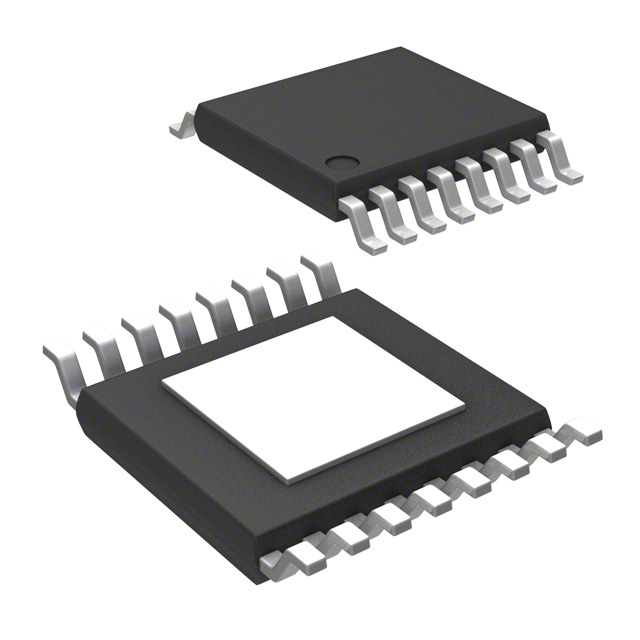
HTSSOP (16)
5.10mm x 6.60mm
(1) 要了解所有可用封装,请参见数据表末尾的可订购产品附录。
典型升压 LED 驱动器应用原理图
D
CIN
CVCC
CSS
1
2
RT
3
VPWM
4
5
CCOMP
RADJ1
6
7
CIMON
8
VIN
SS
RT/SYNC
PWM
COMP
IADJ
Q1
VCC
GATE
IS
PGND
OVP
DDRV
IMON
CSP
AGND
PAD
CSN
100
LED+
VO = 60 V, ILED = 300 mA
ROV2
TPS92691-Q1
RADJ2
效率与输出电压之间的关系
RCS
COUT
95
16
15
ROV1
14
13
12
11
10
RIS
COV
Q2
LEDÅ
Efficiency (%)
VIN
L
90
85
9
80
75
8
9
10
11
12
13
14
VIN (V)
15
16
17
18
D019
1
An IMPORTANT NOTICE at the end of this data sheet addresses availability, warranty, changes, use in safety-critical applications,
intellectual property matters and other important disclaimers. PRODUCTION DATA.
English Data Sheet: SLVSD68
�TPS92691, TPS92691-Q1
ZHCSEM9 – DECEMBER 2015
www.ti.com.cn
目录
1
2
3
4
5
6
7
特性 ..........................................................................
应用 ..........................................................................
说明 ..........................................................................
修订历史记录 ...........................................................
Pin Configuration and Functions .........................
Specifications.........................................................
1
1
1
2
3
4
6.1
6.2
6.3
6.4
6.5
6.6
4
4
4
5
5
7
Absolute Maximum Ratings ......................................
ESD Ratings..............................................................
Recommended Operating Conditions.......................
Thermal Information ..................................................
Electrical Characteristics...........................................
Typical Characteristics ..............................................
7.4 Device Functional Modes........................................ 16
8
Application and Implementation ........................ 17
8.1 Application Information............................................ 17
8.2 Typical Applications ................................................ 26
9 Power Supply Recommendations...................... 37
10 Layout................................................................... 37
10.1 Layout Guidelines ................................................. 37
10.2 Layout Example .................................................... 38
11 器件和文档支持 ..................................................... 39
11.1
11.2
11.3
11.4
11.5
Detailed Description ............................................ 11
7.1 Overview ................................................................. 11
7.2 Functional Block Diagram ....................................... 11
7.3 Feature Description................................................. 12
相关链接................................................................
社区资源................................................................
商标 .......................................................................
静电放电警告.........................................................
Glossary ................................................................
39
39
39
39
39
12 机械、封装和可订购信息 ....................................... 39
4 修订历史记录
2
日期
修订版本
注释
2015 年 12 月
*
首次发布。
Copyright © 2015, Texas Instruments Incorporated
�TPS92691, TPS92691-Q1
www.ti.com.cn
ZHCSEM9 – DECEMBER 2015
5 Pin Configuration and Functions
PWP Package
16-Pin HTSSOP with PowerPAD™
Top View
VIN
1
16
VCC
SS
2
15
GATE
RT/SYNC
3
14
IS
PWM
4
13
PGND
COMP
5
12
OVP
IADJ
6
11
DDRV
IMON
7
10
CSP
AGND
8
9
CSN
Thermal
Pad
Pin Functions
PIN
NO.
NAME
I/O
DESCRIPTION
1
VIN
—
Input supply for the internal VCC regulator. Bypass with 100-nF capacitor to GND located close to the
controller.
2
SS
I/O
Soft-start programming pin. Connect a capacitor to AGND to extend the start-up time. Switching can
be disabled by shorting the pin to GND.
3
RT/SYNC
I/O
Oscillator frequency programming pin. Connect a resistor to AGND to set the switching frequency. The
internal oscillator can be synchronized by coupling an external clock pulse through 100-nF series
capacitor.
4
PWM
I
PWM dimming input. Driving the pin below 2.3 V (typ), turns off switching, idles the oscillator,
disconnects the COMP pin, and sets DDRV output to ground. The input signal duty cycle controls the
average LED current through PWM dimming operation. Connect to VCC when not used for PWM
dimming.
5
COMP
I/O
Transconductance error amplifier output. Connect compensation network to achieve desired closedloop response.
6
IADJ
I
LED current reference input. Connecting pin to VCC with 100-kΩ series resistor sets internal reference
voltage to 2.42 V and the current sense threshold, V(CSP-CSN)to 172 mV. The pin can be modulated by
external voltage source from 0 V to 2.25 V to implement analog dimming.
7
IMON
O
LED current report pin. The LED current sensed by CSP/CSN input is reported as VIMON = 14 × ILED ×
Rcs. Bypass with a 1-nF ceramic capacitor to AGND.
8
AGND
—
Analog ground. Return for the internal voltage reference and analog circuit. Connect to circuit ground,
GND, to complete return path.
9
CSN
I
Current sense amplifier negative input (–). Connect directly to the negative node of LED current sense
resistor RCS).
10
CSP
I
Current sense amplifier positive input (+). Connect directly to the positive node of LED current sense
resistor RCS).
11
DDRV
O
Series dimming FET gate driver output. Connect to gate of external N-channel MOSFET or a level-shift
circuit with P-channel MOSFET to implement series FET PWM dimming.
12
OVP
I
Hysteretic overvoltage protection input. Connect resistor divider from output voltage to set OVP
threshold and hysteresis.
13
PGND
14
IS
I
Switch current sense input. Connected to the switch current sense resistor, RIS, in the source of the Nchannel MOSFET.
15
GATE
O
N-channel MOSFET gate driver output. Connect to gate of external switching N-channel MOSFET.
16
VCC
—
VCC bias supply pin. Locally decouple to PGND using a 2.2-µF to 4.7-µF ceramic capacitor located
close to the controller.
—
The AGND and PGND pin must be connected to the exposed PowerPAD for proper operation. This
PowerPAD must be connected to PCB ground plane using multiple vias for good thermal performance.
PowerPAD
—
Power ground connection pin for internal N-channel MOSFET gate drivers. Connect to circuit ground,
GND, to complete return path.
Copyright © 2015, Texas Instruments Incorporated
3
�TPS92691, TPS92691-Q1
ZHCSEM9 – DECEMBER 2015
www.ti.com.cn
6 Specifications
6.1 Absolute Maximum Ratings
over operating free-air temperature range (unless otherwise noted) (1) (2)
Input voltage
Output voltage (4)
Source current
Sink current
MIN
MAX
UNIT
VIN, CSP, CSN
–0.3
65
V
IADJ, IS, PWM, RT/SYNC
–0.3
8.8
V
OVP, SS
–0.3
5.5
V
CSP to CSN (3), PGND
–0.3
0.3
V
VCC, GATE, DDRV
–0.3
8.8
V
COMP
–0.3
5.0
V
IMON
—
100
µA
GATE, DDRV (Pulsed 2.5 V), the
GATE and DDRV outputs are enabled to ramp the inductor current to the previous steady-state value. The
COMP pin is connected and the error amplifier and oscillator are enabled only when the switch current sense
voltage VIS exceeds the COMP voltage, VCOMP, thus immediately forcing the converter into steady-state
operation with minimum LED current overshoot. The PWM pin should be connected to the VCC if dimming is not
required. An internal pulldown resistor sets the input to logic-low and disables the part when the pin is
disconnected or left floating.
14
Copyright © 2015, Texas Instruments Incorporated
�TPS92691, TPS92691-Q1
www.ti.com.cn
ZHCSEM9 – DECEMBER 2015
Feature Description (continued)
LED-
LED+
TPS92691
TPS92691
DDRV
DDRV
Figure 22. Series Dimming FET Connections
The DDRV output follows the PWM input signal and is capable of sinking and sourcing up to 500 mA of peak
current to control a low-side series connected N-channel dimming FET. Alternatively, the DDRV output can be
translated with an external level-shift circuit to drive a high-side series P-channel dimming FET as shown in
Figure 22. The series dimming FET is required to achieve high contrast ratio as it ensures fast rise and fall times
of the LED current in response to the PWM input. Without any dimming FET, the rise and fall times are limited by
the inductor slew rate and the closed-loop bandwidth of the system. Leave the DDRV pin unconnected if not
used.
7.3.9 Soft-Start
The soft-start feature helps the regulator gradually reach the steady-state operating point, thus reducing startup
stresses and surges. The TPS92691/-Q1 clamps the COMP pin to the SS pin, separated by a diode, until LED
current nears the regulation threshold. The internal 10-µA soft-start current source gradually increases the
voltage on an external soft-start capacitor CSS connected to the SS pin. This results in a gradual rise of the
COMP voltage from GND.
The internal 10-µA current source turns on when VCC exceeds the UVLO threshold. At the beginning of the softstart sequence, the SS pulldown switch is active and is released when the voltage VSS drops below 25 mV. The
SS pin can also be pulled down by an external switch to stop switching. When the SS pin is externally driven to
enable switching, the slew-rate on the COMP pin should be controlled by choosing a compensation capacitor
that avoids large startup transients. The value of CSS should be large enough to charge the output capacitor
during the soft-start transition period.
7.3.10 Current Monitor Output
The IMON pin voltage represents the LED current measured by the rail-to-rail current sense amplifier across the
external current shunt resistor. The linear relationship between the IMON voltage and LED current includes the
amplifier gain-factor of 14 (see Figure 14). The IMON output can be connected to an external microcontroller or
comparator to facilitate LED open, short, or cable harness fault detection and mitigation based on programmable
threshold VOCTH. The IMON voltage is internally clamped to 3.7 V.
TPS92691
SS
PWM
VOCTH
+
IMON
Figure 23. LED Overcurrent Protection using IMON Output
Copyright © 2015, Texas Instruments Incorporated
15
�TPS92691, TPS92691-Q1
ZHCSEM9 – DECEMBER 2015
www.ti.com.cn
Feature Description (continued)
7.3.11 Overvoltage Protection
The TPS92691/-Q1 device includes a dedicated OVP pin which can be used for either input or output
overvoltage protection. This pin features a precision 1.24 V (typ) threshold with 20-µA (typ) of hysteresis current.
The overvoltage threshold limit is set by a resistor divider network from the input or output terminal to GND.
When the OVP pin voltage exceeds the reference threshold, the GATE and DDRV pins are immediately pulled
low and the SS and COMP capacitors are discharged. The GATE is enabled and a new startup sequence is
initiated after the voltage drops below the hysteresis threshold set by the 20-µA source current and the external
resistor divider.
7.3.12 Thermal Protection
Internal thermal shutdown circuitry is implemented to protect the controller in the event the maximum junction
temperature is exceeded. When activated, typically at 175°C, the controller is forced into a shutdown mode,
disabling the internal regulator. This feature is designed to prevent overheating and damage to the device.
7.4 Device Functional Modes
This device has no additional functional modes.
16
Copyright © 2015, Texas Instruments Incorporated
�TPS92691, TPS92691-Q1
www.ti.com.cn
ZHCSEM9 – DECEMBER 2015
8 Application and Implementation
NOTE
Information in the following applications sections is not part of the TI component
specification, and TI does not warrant its accuracy or completeness. TI’s customers are
responsible for determining suitability of components for their purposes. Customers should
validate and test their design implementation to confirm system functionality.
8.1 Application Information
The TPS92691/-Q1 controller is suitable for implementing step-up or step-down LED driver topologies including
Buck, Boost, Buck-Boost, SEPIC, Cuk, and Flyback. Use the following design procedure to select component
values for the TPS92691/-Q1 device. This section presents a simplified discussion of the design process for the
Buck, Boost, and Buck-Boost converter. The expressions derived for Buck-Boost can also be altered to select
components for a 1:1 coupled-inductor SEPIC converter. The design procedure can be easily adapted for
Flyback and Cuk converter topologies.
VIN
L
RCS
D
CIN
CVCC
ROV2
TPS92691-Q1
CSS
RADJ2
1
2
RT
3
VPWM
4
5
CCOMP
6
7
RADJ1
CIMON
8
VIN
Q1
VCC
SS
GATE
RT/SYNC
PWM
IS
PGND
COMP
IADJ
OVP
DDRV
IMON
CSP
AGND
PAD
CSN
LED+
COUT
16
15
ROV1
14
RIS
13
Q2
COV
12
LEDÅ
11
10
9
Figure 24. Boost LED Driver
VIN
L1
CIN
L2
CS
CVCC
TPS92691-Q1
CSS
RADJ2
1
2
RT
3
VPWM
4
5
CCOMP
RADJ1
6
7
CIMON
8
VIN
VCC
SS
GATE
RT/SYNC
PWM
IS
PGND
COMP
IADJ
D
OVP
DDRV
IMON
CSP
AGND
PAD
CSN
Q1
16
ROV2
ROV1
14
12
LED+
COUT
15
13
RCS
RIS
COV
Q2
LEDÅ
11
10
9
Figure 25. SEPIC LED Driver
Copyright © 2015, Texas Instruments Incorporated
17
�TPS92691, TPS92691-Q1
ZHCSEM9 – DECEMBER 2015
www.ti.com.cn
Application Information (continued)
RCS
COUT
VIN
L
D
CIN
ROV2
LEDÅ
Q2
LED+
RLS2
CVCC
TPS92691-Q1
CSS
RADJ2
1
2
RT
3
VPWM
4
5
CCOMP
6
7
RADJ1
CIMON
8
VIN
Q1
VCC
SS
GATE
RT/SYNC
PWM
IS
PGND
COMP
IADJ
OVP
DDRV
IMON
CSP
AGND
PAD
CSN
Q4
16
Q3
15
14
ROV1
RIS
13
RLS1
COV
12
11
10
9
Figure 26. Buck-Boost LED Driver
VIN
LED+
RLS2 Q2
D ROV2
CIN
L
CVCC
TPS92691-Q1
CSS
RADJ2
1
2
RT
3
VPWM
4
5
CCOMP
RADJ1
6
7
CIMON
8
VIN
SS
RT/SYNC
PWM
COMP
IADJ
Q1
VCC
GATE
IS
PGND
OVP
DDRV
IMON
CSP
AGND
PAD
CSN
COUT
RCS
Q4
16
Q3
15
14
13
12
LEDÅ
ROV1
RIS
RLS1
COV
11
10
9
Figure 27. Buck LED Driver
18
Copyright © 2015, Texas Instruments Incorporated
�TPS92691, TPS92691-Q1
www.ti.com.cn
ZHCSEM9 – DECEMBER 2015
Application Information (continued)
8.1.1 Duty Cycle Considerations
The switch duty cycle, D, defines the converter operation and is a function of the input and output voltages. In
steady state, the duty cycle is derived using expression:
Buck:
D
VO
VIN
(2)
Boost:
D
VO
VIN
VO
(3)
Buck-Boost:
D
VO
VIN
VO
(4)
The minimum duty cycle, DMIN, and maximum duty cycle, DMAX, are calculated by substituting maximum input
voltage, VIN(MAX), and the minimum input voltage, VIN(MIN), respectively in the previous expressions. The minimum
duty cycle achievable by the device is determined by the leading edge blanking period and the switching
frequency. The maximum duty cycle is limited by the internal oscillator to 93% (typ) to allow for minimum off-time.
It is necessary for the operating duty cycle to be within the operating limits of the device to ensure closed-loop
LED current regulation over the specified input and output voltage range.
8.1.2 Inductor Selection
The inductor peak-to-peak ripple current, ΔiL-PP, is typically set between 10% and 80% of the maximum inductor
current, IL, as a good compromise between core loss and copper loss of the inductor. Higher ripple inductor
current allows a smaller inductor size, but places more of a burden on the output capacitor to smooth the LED
current ripple. Knowing the desired ripple ratio RR, switching frequency ƒSW, maximum duty cycle DMAX, and the
typical LED current ILED, the inductor value can be calculated as follows:
Buck:
'iL(PP)
L
RR ˜ IL
VIN(MIN)
RR ˜ ILED
(5)
VO u DMAX
'iL(PP) u fSW
(6)
Boost and Buck-Boost:
'iL(PP)
L
RR ˜ IL
RR ˜
ILED
1 DMAX
(7)
VIN(MIN) u DMAX
'iL(PP) u fSW
(8)
As an alternative, the inductor can be selected based on CCM-DCM boundary condition specified based on
output power, PO(BDRY). The choice of inductor ensures CCM operation in battery-powered LED driver
applications that are designed to support different LED string configurations with a wide range of programmable
LED current setpoints. The output power should be calculated based on the lowest LED current and the lowest
output voltage requirements for a given application.
PO(BDRY) d ILED(MIN) u VO(MIN)
(9)
Buck:
L
2
VO(MAX)
2 u PO(BDRY) u fSW
VO(MAX)
§
u ¨¨ 1
VIN
©
·
¸¸
¹
(10)
Boost:
Copyright © 2015, Texas Instruments Incorporated
19
�TPS92691, TPS92691-Q1
ZHCSEM9 – DECEMBER 2015
www.ti.com.cn
Application Information (continued)
L
§
VIN
u ¨1
¨
V
O(MAX)
©
2
VIN
2 u PO(BDRY) u fSW
·
¸
¸
¹
(11)
Buck-Boost:
1
L
2 u PO(BDRY) u fSW
§
1
u¨
¨ VO(MAX)
©
1 ·
¸
VIN ¸¹
2
(12)
The saturation current rating of the inductor should be greater than the peak inductor current, IL(PK), at the
maximum operating temperature.
VIN(MIN) u DMAX
IL(PK) IL
2 u L u fSW
(13)
8.1.3 Output Capacitor Selection
The output capacitors are required to attenuate the discontinuous or large ripple current generated by switching
and achieve the desired peak-to-peak LED current ripple, ΔiLED(PP). The capacitor value depends on the total
series resistance of the LED string, rD, the switching frequency, ƒSW, and on the converter topology (that is, stepup or step-down). For the Buck and Cuk topology, the inductor is in series with LED load and requires a smaller
capacitor than the Boost, Buck-Boost, and SEPIC topologies to achieve the same LED ripple current. The
capacitance required for the target LED ripple current can be calculated based on following equations.
Buck:
COUT
'iL(PP)
8 u fSW u rD u 'iLED(PP)
Boost and Buck-Boost:
ILED u DMAX
COUT
fSW u rD u 'iLED(PP)
(14)
(15)
When choosing the output capacitors, it is important to consider the ESR and the ESL characteristics as they
directly impact the LED current ripple. Ceramic capacitors are the best choice due to their low ESR, high ripple
current rating, long lifetime, and good temperature performance. When selecting ceramic capacitors, it is
important to consider the derating factors associated with higher temperature and DC bias operating conditions.
TI recommends an X7R dielectric with voltage rating greater than maximum LED stack voltage. An aluminum
electrolytic capacitor can be used in parallel with ceramic capacitors to provide bulk energy storage. The
aluminum capacitors must have necessary RMS current and temperature ratings to ensure prolonged operating
lifetime. The minimum allowable RMS output capacitor current rating, ICOUT(RMS), can be approximated:
Buck:
ICOUT(RMS)
'iLED(PP)
12
(16)
Boost and Buck-Boost:
ICOUT(RMS)
ILED u
DMAX
1 DMAX
(17)
The expressions (Equation 14 to Equation 17) are best suited for designs driving a fixed LED load, with known
output voltage and LED current. For applications that are required to support different LED string configurations
with a wide range of programmable LED current setpoints, the previous expressions are rearranged to reflect
output capacitance based on the maximum output power, PO(MAX), to ensure that LED current ripple
specifications are met over the entire range of operation. Typical Buck-Boost LED Driver provides the details for
Buck-Boost LED driver.
20
Copyright © 2015, Texas Instruments Incorporated
�TPS92691, TPS92691-Q1
www.ti.com.cn
ZHCSEM9 – DECEMBER 2015
Application Information (continued)
8.1.4 Input Capacitor Selection
The input capacitors, CIN, smooth the input voltage ripple and store energy to supply input current during input
voltage or PWM dimming transients. The series inductor in the Boost, SEPIC, and Cuk topology provides
continuous input current and requires a smaller input capacitor to achieve desired input ripple voltage, ΔvIN(PP).
The Buck and Buck-Boost topology have discontinuous input current and require a larger capacitor to achieve
the same input voltage ripple. Based on the switching frequency, ƒSW, and the maximum duty cycle, DMAX, the
input capacitor value can be calculated as follows:
Buck:
CIN
ILED u DMAX u (1 DMAX )
fSW u 'vIN(PP)
(18)
Boost:
CIN
'iL(PP)
8 u fSW u 'vIN(PP)
(19)
Buck-Boost:
CIN
ILED u DMAX
fSW u 'vIN(PP)
(20)
X7R dielectric-based ceramic capacitors are the best choice due to their low ESR, high ripple current rating, and
good temperature performance. For applications using PWM dimming, TI recommends an aluminum electrolytic
capacitor in addition to ceramic capacitors to minimize the voltage deviation due to large input current transients
generated in conjunction with the rising and falling edges of the LED current.
TPS92691
R VIN
VIN
CVIN
Figure 28. VIN Filter
For most applications, TI highly recommends to bypass the VIN pin with a 0.1-µF ceramic capacitor placed as
close as possible to the device and add a series 10-Ω resistor to create a 150-kHz low-pass filter and eliminate
undesired high-frequency noise.
8.1.5 Main Power MOSFET Selection
The power MOSFET should be able to sustain the maximum switch node voltage, VSW, and switch RMS current
derived based on the converter topology. TI recommends a drain voltage VDS rating of at least 20% greater than
the maximum switch node voltage to ensure safe operation. The MOSFET drain-to-source breakdown voltage,
VDS, and RMS current ratings are calculated using the following expressions.
Buck:
VDS
VIN(MAX) u 1.2
IQ(RMS)
Boost:
VDS
ILED u DMAX
VO(OV) u 1.2
Copyright © 2015, Texas Instruments Incorporated
(21)
(22)
(23)
21
�TPS92691, TPS92691-Q1
ZHCSEM9 – DECEMBER 2015
www.ti.com.cn
Application Information (continued)
IQ(RMS)
ILED u
DMAX
1 DMAX
(24)
Buck-Boost:
VDS
VIN(MAX)
IQ(RMS)
ILED u
VO(OV) u 1.2
(25)
DMAX
1 DMAX
(26)
Where the voltage, VO(OV), is the overvoltage protection threshold and the worst-case output voltage under fault
conditions.
Select a MOSFET with low total gate charge, Qg, to minimize gate drive and switching losses. The MOSFET RDS
resistance is usually a less critical parameter because the switch conduction losses are not a significant part of
the total converter losses at high operating frequencies. The switching and conduction losses are calculated as
follows:
PCOND
PSW
2
RDS u IQ(RMS)
2
IL u VSW
(27)
u CRSS u fSW
IGATE
(28)
CRSS is the MOSFET reverse transfer capacitance. IL is the average inductor current. IGATE is gate drive output
current, typically 500 mA. The MOSFET power rating and package should be selected based on the total
calculated loss, the ambient operating temperature, and maximum allowable temperature rise.
8.1.6 Rectifier Diode Selection
A Schottky diode (when used as a rectifier) provides the best efficiency due to low forward voltage drop and
near-zero reverse recovery time. TI recommends a diode with a reverse breakdown voltage, VD(BR), greater than
or equal to MOSFET drain-to-source voltage, VDS, for reliable performance. It is important to understand the
leakage current characteristics of the Schottky diode, especially at high operating temperatures because it
impacts the overall converter operation and efficiency.
The current through the diode, ID, is given by:
ID
IL u (1
DMAX )
(29)
The diode should be sized to exceed the current rating, and the package should be able to dissipate power
without exceeding the maximum allowable temperature.
8.1.7
LED Current Programming
The LED current is set by the external current sense resistor, RCS, and the analog adjust voltage, VIADJ. The
current sense resistor is placed in series with the LED load and can be located either on the high side
(connected to the output, VO), or on the low side (connected to ground, GND). The CSP and CSN inputs of the
internal rail-to-rail current sense amplifier are connected to the RCS resistor to enable closed-loop regulation.
When VIADJ > 2.5 V, the internal 2.42-V reference sets the V(CSP-CSN) threshold to 172 mV and the LED current is
regulated to:
0.172
ILED
RCS
(30)
The LED current can be programmed by varying VIADJ between 140 mV to 2.25 V. The LED current can be
calculated using:
VIADJ
ILED
14 u RCS
(31)
22
Copyright © 2015, Texas Instruments Incorporated
�TPS92691, TPS92691-Q1
www.ti.com.cn
ZHCSEM9 – DECEMBER 2015
Application Information (continued)
The output voltage ripple should be limited to 50 mV for best performance. TI recommends a low-pass commonmode filter consisting of 10-Ω resistors is series with CSP and CSN inputs and 0.01-µF capacitors to ground to
minimize the impact of voltage ripple and noise on LED current accuracy (see Figure 20). A 0.1-µF capacitor
across CSP and CSN is included to filter high-frequency differential noise.
8.1.8 Switch Current Sense Resistor and Slope Compensation
The switch current sense resistor, RIS, is used to implement peak current mode control and to set the peak
switch current limit. The value of switch current sense RIS is selected to achieve stable inner current loop
operation based on the magnitude of slope compensation ramp, VSL, and to protect the main switching MOSFET
under fault conditions. The lower of the two values calculated using the following equations should be selected
for RIS.
2 u VSL u L u fSW
RIS
VO(MAX)
(32)
RIS
VIS(LIMIT)
VSL u DMAX
IL(PK)
(33)
The internal slope compensation voltage, VSL is fixed at 200 mV (typ). A resistor can be placed in series with the
IS pin to increase slope compensation, if necessary. The peak switch current limit is set based on the internal
current limit threshold of 525 mV (typ) and adjusted based on slope compensation to ensure reliable operation
while PWM dimming.
TPS92691
VCC
GATE
100 O
IS
PGND
RIS
1 nF
Figure 29. IS Input Filter
The use of a 1-nF and 100-Ω low-pass filter is optional. If used, the resistor value should be less than 500 Ω to
limit its influence on the internal slope compensation signal.
8.1.9 Feedback Compensation
The open-loop response is the product of the modulator transfer function (shown in Equation 34) and the
feedback transfer function. Using a first-order approximation, the modulator transfer function can be modeled as
a single pole created by the output capacitor, and in the boost and buck-boost topologies, a right half-plane zero
created by the inductor, where both have a dependence on the LED string dynamic resistance, rD. Because TI
recommends a ceramic capacitor, the ESR of the output capacitor is neglected in the analysis. The small-signal
modulator model also includes a DC gain factor that is dependent on the duty cycle, output voltage, and LED
current.
§
s ·
¨1
¸
Öi
ZZ ¹
©
LED
G0
vÖ COMP
§
s ·
¨1
¸
ZP ¹
©
(34)
Table 1 summarizes the expression for the small-signal model parameters.
Copyright © 2015, Texas Instruments Incorporated
23
�TPS92691, TPS92691-Q1
ZHCSEM9 – DECEMBER 2015
www.ti.com.cn
Application Information (continued)
The feedback transfer function includes the current sense resistor and the loop compensation of the
transconductance amplifier. A compensation network at the output of the error amplifier is used to configure loop
gain and phase characteristics. A simple capacitor, CCOMP, from COMP to GND (as shown in Figure 30) provides
integral compensation and creates a pole at the origin. Alternatively, a network of RCOMP, CCOMP, and CHF, shown
in Figure 31, can be used to implement proportional and integral (PI) compensation and to create a pole at the
origin, a low-frequency zero, and a high-frequency pole.
Table 1. Small-Signal Model Parameters
DC GAIN (G0)
POLE FREQUENCY (ωP)
ZERO FREQUENCY (ωZ)
1
1
rD u COUT
—
Buck
(1 D) u VO
Boost
RIS u VO
VO
rD u ILED
VO u rD u COUT
(1 D) u VO
Buck-Boost
RIS u VO
VO u (1 D)2
L u ILED
rD u ILED
VO
D u rD u ILED
VO u (1 D)2
D u L u ILED
D u rD u ILED
VO u rD u COUT
The feedback transfer function is defined as follows.
Feedback transfer function with integral compensation:
vÖ COMP 14 u gM u RCS
Öi
s u CCOMP
(35)
Feedback transfer function with proportional integral compensation:
1 s u RCOMP u CCOMP
vÖ COMP
14 u gM u RCS
Öi
s u CCOMP CHF §
§C
u CHF · ·
LED
¨¨ 1 s u R COMP u ¨ COMP
¸ ¸¸
© CCOMP CHF ¹ ¹
©
(36)
LED
The pole at the origin minimizes output steady-state error. High bandwidth is achieved with the PI compensator
by placing the low-frequency zero an order of magnitude less than the crossover frequency. Use the following
expressions to calculate the compensation network.
TPS92691
TPS92691
COMP
COMP
RCOMP
CCOMP
CSP
ILED
VCC
CSN
GAIN = 14
CSP
+
RCS
+
+
CHF
CCOMP
GAIN = 14
+
RCS
ILED
CURRENT SENSE
AMPLIFIER
VCC
IADJ
CSN
CURRENT SENSE
AMPLIFIER
IADJ
+
+
2.42V
Figure 30. Integral Compensation
2.42V
Figure 31. Proportional-Integral Compensation
Buck with integral compensator:
CCOMP
8.75 u 10 3 u RCS
ZP
(37)
Boost and Buck-Boost with proportional integral compensator:
24
Copyright © 2015, Texas Instruments Incorporated
�TPS92691, TPS92691-Q1
www.ti.com.cn
CCOMP
CHF
RCOMP
ZHCSEM9 – DECEMBER 2015
8.75 u 10
3
§ R u G0 ·
u ¨ CS
¸
ZZ
©
¹
CCOMP
100
(38)
(39)
1
ZP u CCOMP
(40)
The loop response is verified by applying step input voltage transients. The goal is to minimize LED current
overshoot and undershoot with a damped response. Additional tuning of the compensation network may be
necessary to optimize PWM dimming performance.
8.1.10 Soft-Start
The soft-start time (tSS) is the time required for the LED current to reach the target setpoint. The required softstart time, tSS, is programmed using a capacitor, CSS, from SS pin to GND, and is based on the LED current,
output capacitor, and output voltage.
§
COUT u VOUT ·
CSS 12.5 u 10 6 ¨ t SS
¸
ILED
©
¹
(41)
8.1.11 Overvoltage Protection
The overvoltage threshold is programmed using a resistor divider, ROV2 and ROV1, from the output voltage, VO, to
ground for Boost and SEPIC topologies, as shown in Figure 24 and Figure 25. If the LEDs are referenced to a
potential other than ground, as in the Buck-Boost or Buck configuration, the output voltage is sensed and
translated to ground by using a PNP transistor and level-shift resistors, as shown in Figure 27 and Figure 26.
The overvoltage turn-off threshold, VO(OV), is:
Boost:
VO(OV)
§R
ROV2 ·
VOVP(THR) u ¨ OV1
¸
ROV1
©
¹
(42)
Buck and Buck-Boost:
VO(OV)
VOVP(THR) u
ROV2
ROV1
0.7
The overvoltage hysteresis, VOV(HYS) is:
VOV(HYS) IOVP(HYS) u ROV2
(43)
(44)
8.1.12 PWM Dimming Considerations
When PWM dimming, the TPS92691/-Q1 requires another MOSFET placed in series with the LED load. This
MOSFET should have a voltage rating greater than the output voltage, VO, and a current rating at least 10%
higher than the nominal LED current, ILED.
It is important to control the slew-rate of the external FET to achieve a damped LED current response to PWM
rising-edge transitions. For a low-side, N-channel dimming FET, the slew-rate is controlled by placing a resistor
in series with the GATE pin. The rise and fall times depend on the value of the resistor and the gate-to-source
capacitance of the MOSFET. The series resistor can be bypassed with a diode for fast rise time and slow fall
times to achieve 100:1 or higher contrast ratios. If a high-side P-channel dimming FET is used, the rise and fall
times can be controlled by selecting appropriate resistors for the level-shift network, RLS1 and RLS2, as shown in
Figure 26.
Copyright © 2015, Texas Instruments Incorporated
25
�TPS92691, TPS92691-Q1
ZHCSEM9 – DECEMBER 2015
www.ti.com.cn
8.2 Typical Applications
8.2.1 Typical Boost LED Driver
Figure 32. Boost LED Driver With High-Side Current Sense
26
Copyright © 2015, Texas Instruments Incorporated
�TPS92691, TPS92691-Q1
www.ti.com.cn
ZHCSEM9 – DECEMBER 2015
8.2.1.1 Design Requirements
Table 2 shows the design parameters for the boost LED driver application.
Table 2. Design Parameters
PARAMETER
TEST CONDITIONS
MIN
TYP
MAX
7
14
18
UNIT
INPUT CHARACTERISTICS
Input voltage range
Input UVLO setting
V
4.5
V
LED forward voltage
3.2
V
Number of LEDs in series
12
OUTPUT CHARACTERISTICS
VO
Output voltage
38.4
V
ILED
Output current
LED+ to LED–
500
mA
RR
LED current ripple ratio
5%
rD
LED string resistance
Ω
4
Maximum output power
20
PWM dimming range
240-Hz PWM frequency
4%
25
W
100%
SYSTEMS CHARACTERISTICS
ΔiL(PP)
Inductor current ripple
ΔvIN(PP)
Input voltage ripple
70
mV
VO(OV)
Output overvoltage protection threshold
50
V
VOV(HYS)
Output overvoltage protection hysteresis
5
V
tss
Soft-start period
8
ms
390
kHz
20%
Switching frequency
8.2.1.2 Detailed Design Procedure
This procedure is for the boost LED driver application.
8.2.1.2.1 Calculating Duty Cycle
Solve for D, DMAX, and DMIN:
VO VIN 38.4 14
D
VO
38.4
DMAX
DMIN
VO
VIN(MIN)
(45)
38.4 7
38.4
VO
VO
0.6354
VIN(MAX)
0.8177
(46)
38.4 18
38.4
VO
0.5312
(47)
8.2.1.2.2 Setting Switching Frequency
Solve for RT:
1.432 u 1010
RT
1.047
fSW
1.432 u 1010
390 u 10
3
1.047
20.05 u 103
(48)
The closest standard resistor of 20 kΩ is selected.
8.2.1.2.3 Inductor Selection
The inductor value should ensure continuous conduction mode (CCM) of operation and should achieve desired
ripple specification, ΔiL(PP).
Copyright © 2015, Texas Instruments Incorporated
27
�TPS92691, TPS92691-Q1
ZHCSEM9 – DECEMBER 2015
'iL(PP)
RR u
www.ti.com.cn
ILED
1 DMAX
Solving for inductor:
VIN(MIN) u DMAX
L
'iL(PP) u fSW
0.2 u
0.5
1 0.8177
7 u 0.8177
0.5485 u 390 u 103
0.5485
(49)
26.76 u 10
6
(50)
The closest standard inductor is 27 µH. The expected inductor ripple based on the chosen inductor is:
VIN(MIN) u DMAX
7 u 0.8177
0.5436
'iL(PP)
L u fSW
27 u 10 6 u 390 u 103
(51)
The inductor saturation current rating should be greater than the peak inductor current, IL(PK).
VIN(MIN) u DMAX
ILED
0.5
7 u 0.8177
IL(PK)
3.01
1 DMAX
2 u L u fSW
1 0.8177 2 u 27 u 10 6 u 390 u 103
(52)
8.2.1.2.4 Output Capacitor Selection
The specified peak-to-peak LED current ripple, ΔiLED(PP), is:
'iLED(PP) 0.05 u ILED 25 u 10 3
(53)
The output capacitance required to achieve the target LED current ripple is:
ILED u DMAX
0.5 u 0.8177
COUT
10.48 u 10 6
fSW u rD u 'iLED(PP) 390 u 103 u 4 u 25 u 10 3
(54)
Considering 40% derating factor under DC bias operation, four 4.7-µF, 100-V rated X7R ceramic capacitors are
used in parallel to achieve a combined output capacitance of 18.8 µF.
8.2.1.2.5 Input Capacitor Selection
The input capacitor is required to reduce switching noise conducted through the input wires and reduced the
input impedance of the LED driver. The capacitor required to limit peak-to-peak input ripple voltage ripple,
ΔvIN(PP), to 70 mV is given by:
'iL(PP)
0.5436
CIN
2.49 u 10 6
8 u fSW u 'vIN(PP) 8 u 390 u 103 u 70 u 10 3
(55)
A 4.7-µF, 50-V X7R ceramic capacitor is selected.
8.2.1.2.6 Main N-Channel MOSFET Selection
The MOSFET ratings should exceed the maximum output voltage and RMS switch current given by:
VDS VO(OV) u 1.2 50 u 1.2 60
IQ(RMS)
ILED u
DMAX
1 DMAX
0.5 u
0.8177
1 0.8177
(56)
2.48
(57)
A 60-V or a 100-V N-channel MOSFET with current rating exceeding 3 A is required for this design.
8.2.1.2.7 Rectifying Diode Selection
The diode should be selected based on the following voltage and current ratings:
VD(BR) VO(OV) u 1.2 50 u 1.2 60
ID
IL u (1 DMAX ) ILED
0.5
(58)
(59)
A 60-V or a 100-V Schottky diode with low reverse leakage current is suitable for this design. The package must
be able to handle the power dissipation resulting from continuous forward current, ID, of 0.5 A.
28
Copyright © 2015, Texas Instruments Incorporated
�TPS92691, TPS92691-Q1
www.ti.com.cn
ZHCSEM9 – DECEMBER 2015
8.2.1.2.8 Programming LED Current
LED current is based on the current shunt resistor, RCS and the V(CSP-CSN) threshold set by the voltage on the
IADJ pin VIADJ. By default, IADJ is tied to VCC via an external resistor to enable the internal reference voltage of
2.42 V that then sets the V(CSP-CSN) threshold to 172 mV. The current shunt resistor value is calculated by:
0.172 0.172
RCS
0.344
ILED
0.5
(60)
Two 0.68-Ω resistors are connected in parallel to achieve RCS of 0.34 Ω.
8.2.1.2.9 Setting Switch Current Limit and Slope Compensation
The switch current sense resistor, RIS, is calculated by solving the following equations and choosing the lowest
value:
RIS
RIS
2 u VSL u L u fSW
VO(MAX)
VIS(LIMIT)
2 u 0.2 u 27 u 10 6 u 390 u 103
38.4
VSL u DMAX
IL(PK)
0.525 0.2 u 0.8177
3.01
0.11
(61)
0.12
(62)
A standard value of 0.1 Ω is selected.
8.2.1.2.10 Deriving Compensator Parameters
The modulator transfer function for the Boost converter is derived for nominal VIN voltage and corresponding duty
cycle, D, and is given by the following equation. (See Table 1 for more information.)
Öi
LED
vÖ COMP
§
s ·
¨1
¸
ZZ ¹
©
G0
§
s ·
¨1
¸
Z
P ¹
©
s
§
·
¨1
¸
378.12 u 103 ¹
©
3.466
s
§
·
¨1
3 ¸
u
14
10
©
¹
(63)
The proportional-integral compensator components CCOMP and RCOMP are obtained by solving the following
expressions:
3
§ R u G0 ·
u ¨ CS
¸ 8.75 u 10
ZZ
©
¹
1
CCOMP
8.75 u 10
RCOMP
1
ZP u CCOMP
14 u 103 u 33 u 10
9
3
§ 0.34 u 3.466 ·
u¨
¸
© 378.12 u 103 ¹
27.27 u 10
9
(64)
2.165 u 103
(65)
The closet standard capacitor of 33 nF and resistor of 2.15 kΩ is selected. The high frequency pole location is
set by a 100 pF CHF capacitor.
8.2.1.2.11 Setting Start-up Duration
The soft-start capacitor required to achieve start-up in 8 ms is given by:
CSS
12.5 u 10
6
§
¨ t SS
©
COUT u VOUT ·
¸
ILED
¹
12.5 u 10
6
§
¨ 8 u 10
¨
©
3
18.8 u 10 6 u 38.4 ·
¸
¸
0.5
¹
81.9 u 10
9
(66)
The closet standard capacitor of 100 nF is selected.
8.2.1.2.12 Setting Overvoltage Protection Threshold
The overvoltage protection threshold of 50 V and hysteresis of 5 V is set by the ROV1 and ROV2 resistor divider.
VOV(HYS)
5
ROV2
250 u 103
6
20 u 10
20 u 10 6
(67)
Copyright © 2015, Texas Instruments Incorporated
29
�TPS92691, TPS92691-Q1
ZHCSEM9 – DECEMBER 2015
ROV1
www.ti.com.cn
§
·
1.24
¨
¸R
¨ VO(OV) 1.24 ¸ OV2
©
¹
§ 1.24 ·
3
¨ 50 1.24 ¸ 250 u 10
©
¹
6.36 u 103
(68)
The standard resistor values of 249 kΩ and 6.34 kΩ are chosen.
8.2.1.2.13 PWM Dimming Considerations
A series dimming FET is required to meet PWM dimming specification from 100% to 4% duty cycle. A 60-V, 2-A
N-channel FET is suitable for this application.
As an alternative, a 60-V, 2-A P-channel FET could be used to achieve PWM dimming. An external level-shift
circuit is required to translate the DDRV signal to the gate of the P-channel dimming FET. The drive strength of 5
mA and gate-source voltage of 15 V are set by the 1-kΩ and 2-kΩ level-translator resistors and a small-signal Nchannel MOSFET, whose gate is connected to DDRV.
By default, the PWM pin is connected to VCC through a 100-kΩ resistor to enable the part upon start-up.
8.2.1.3 Application Curves
These curves are for the boost LED driver.
100
Efficiency (%)
95
90
85
80
75
7
8
9
10
11
12 13
VIN (V)
14
15
16
Figure 33. Efficiency vs Input Voltage
Ch1: Input voltage; Ch2: Soft-start (SS) voltage;
Ch3: Input current;
Ch4: LED current; Time: 2 ms/div
Figure 35. Startup Transient
30
17
18
D021
Ch1: Switch node voltage;
Ch3: Switch sense current resistor voltage;
Ch4: LED current; Time: 1 µs/div
Figure 34. Normal Operation
Ch1: Output voltage;
Ch2: Soft-start (SS) voltage;
Ch4: LED current; Time: 200 ms/div
Figure 36. Overvoltage Protection
Copyright © 2015, Texas Instruments Incorporated
�TPS92691, TPS92691-Q1
www.ti.com.cn
ZHCSEM9 – DECEMBER 2015
Ch1: GATE voltage; Ch2: External CLK signal;
Ch3: Switch sense current resistor voltage;
Ch4: LED current; Time: 1 µs/div
Figure 37. Clock Synchronization
Ch1: DDRV voltage; Ch2: PWM input;
Ch3: Switch sense current resistor voltage;
Ch4: LED current; Time: 2 ms/div
Figure 38. PWM Dimming Transient
Ch1: DDRV voltage; Ch2: PWM input;
Ch3: Switch sense current resistor voltage;
Ch4: LED current; Time: 4 µs/div
Figure 39. PWM Dimming Transient (Zoomed)
Ch1: Input voltage;
Ch2: IMON voltage;
Ch4: LED current; Time: 2 ms/div
Figure 40. Step Input Voltage Transient and IMON
Behavior
Copyright © 2015, Texas Instruments Incorporated
31
�TPS92691, TPS92691-Q1
ZHCSEM9 – DECEMBER 2015
www.ti.com.cn
8.2.2 Typical Buck-Boost LED Driver
Figure 41. Buck-Boost LED Driver
32
Copyright © 2015, Texas Instruments Incorporated
�TPS92691, TPS92691-Q1
www.ti.com.cn
ZHCSEM9 – DECEMBER 2015
8.2.2.1 Design Requirements
Buck-Boost LED drivers provide the flexibility needed in applications that support multiple LED load
configurations. For such applications, it is necessary to modify the design procedure presented in Application
Information to account for the wider range of output voltage and LED current specifications. This design is based
on the maximum output power PO(MAX), set by the lumen output specified for the lighting application. The design
procedure for a battery connected application with 3 to 9 LEDs in series and maximum 15 W output power is
outlined in this section.
For applications that have a fixed number of LEDs and a narrow LED current range (for brightness correction),
design equations provided in the Application Information and simplified design procedure, similar to one outlined
in Typical Boost LED Driver for Boost LED driver, are recommended for developing an optimized circuit with
lower Bill of Material (BOM) cost.
Table 3. Design Parameters
PARAMETER
TEST CONDITIONS
MIN
TYP
MAX
7
14
18
UNIT
INPUT CHARACTERISTICS
Input voltage range
Input UVLO setting
V
4.5
V
3.2
V
OUTPUT CHARACTERISTICS
LED forward voltage
Number of LEDs in series
VO
Output voltage
ILED
Output current
ΔiLED(PP)
LED current ripple
rD
LED string resistance
PO(MAX)
Maximum output power
LED+ to LED–
3
6
9
9.6
19.2
28.8
V
500
750
1500
mA
5%
1
PWM dimming range
240-Hz PWM frequency
2
4%
3
Ω
15
W
100%
SYSTEMS CHARACTERISTICS
PO(BDRY)
Output power at CCM-DCM boundary
condition
5
W
ΔvIN(PP)
VO(OV)
Input voltage ripple
70
mV
Output overvoltage protection threshold
40
V
VOV(HYS)
Output overvoltage protection hysteresis
5
V
tss
Soft-start period
8
ms
390
kHz
Switching frequency
8.2.2.2 Detailed Design Procedure
8.2.2.2.1 Calculating Duty Cycle
Solving for D, DMAX, and DMIN:
VO
19.2
D
VO VIN 19.2 14
DMAX
DMIN
VO(MAX)
VO(MAX)
VIN(MIN)
VO(MIN)
VO(MIN)
VIN(MAX)
0.5783
(69)
28.8
28.8 7
0.8045
9.6
9.6 18
0.3478
(70)
(71)
8.2.2.2.2 Setting Switching Frequency
Solving for RT resistor:
Copyright © 2015, Texas Instruments Incorporated
33
�TPS92691, TPS92691-Q1
ZHCSEM9 – DECEMBER 2015
RT
www.ti.com.cn
1.432 u 1010
fSW
1.047
1.432 u 1010
390 u 10
3
20.05 u 103
1.047
(72)
8.2.2.2.3 Inductor Selection
The inductor is selected to meet the CCM-DCM boundary power requirement, PO(BDRY). Typically, the boundary
condition is set to enable CCM operation at the lowest possible operating power based on minimum LED forward
voltage drop and LED current. In most applications, PO(BDRY) is set to be 1/3 of the maximum output power,
PO(MAX). The inductor value is calculated for maximum input voltage, VIN(MAX), and output voltage, VO(MAX):
1
1
L
31.46 u 10 6
2
2
1 ·
§
·
§ 1
1
1
2 u 5 u 390 u 103 u ¨
2 u PO(BDRY) u fSW u ¨
¸
¸
¨ VO(MAX) VIN(MAX) ¸
© 28.8 18 ¹
©
¹
(73)
The closest standard value of 33 µH is selected. The inductor ripple current is given by:
VIN(MIN) u DMAX
7 u 0.8045
0.4376
'iL(PP)
L u fSW
33 u 10 6 u 390 u 103
(74)
The inductor saturation rating should exceed the calculated peak current which is based on the maximum output
power using the following expression:
IL(PK)
IL(PK)
§
1
PO(MAX) u ¨
¨ VO(MIN)
©
§ 1
15 u ¨
© 9.6
1·
7 ¸¹
1
VIN(MIN)
·
¸
¸
¹
VO(MIN) u VIN(MIN)
2 u L u fSW u VO(MIN)
9.6 u 7
2 u 33 u 10
6
u 390 u 103 u 9.6 7
VIN(MIN)
(75)
3.863
8.2.2.2.4 Output Capacitor Selection
The output capacitor should be selected to achieve the 5% peak-to-peak LED current ripple specification. Based
on the maximum power, the capacitor is calculated as follows:
PO(MAX)
COUT
fSW u rD(MIN) u 'i LED(PP)u VO(MIN) VIN(MIN)
(76)
COUT
15
30.9 u 10
3
6
390 u 10 u 1u 0.075 u 9.6 7
A minimum of four 10-µF, 50-V X7R ceramic capacitors in parallel are needed to meet the LED current ripple
specification over the entire range of output power. Additional capacitance may be required based on the
derating factor under DC bias operation.
8.2.2.2.5 Input Capacitor Selection
The input capacitor is calculated based on the peak-to-peak input ripple specifications, ΔvIN(PP). The capacitor
required to limit the ripple to 70 mV over range of operation is calculated using:
PO(MAX)
15
CIN
33.1u 10 6
3
fSW u 'v IN(PP)u VO(MIN) VIN(MIN)
390 u 10 u 0.07 u 9.6 7
(77)
A parallel combination of four 10-µF, 50-V X7R ceramic capacitors are used for a combined capacitance of 40
µF. Additional capacitance may be required based on the derating factor under DC bias operation.
8.2.2.2.6 Main N-Channel MOSFET Selection
Calculating the minimum transistor voltage and current rating:
VDS
34
1.2 u VO(OV)
VIN(MAX)
1.2 u (40 18)
69.6
(78)
Copyright © 2015, Texas Instruments Incorporated
�TPS92691, TPS92691-Q1
www.ti.com.cn
IQ(RMS)
ZHCSEM9 – DECEMBER 2015
PO(MAX) §
VIN(MIN) ·
¨1
¸
VIN(MIN) ¨©
VO(MIN) ¸¹
15 §
7 ·
1
7 ¨© 9.6 ¸¹
2.82
(79)
This application requires a 60-V or 100-V N-channel MOSFET with a current rating exceeding 3 A.
8.2.2.2.7 Rectifier Diode Selection
Calculating the minimum Schottky diode voltage and current rating:
VD(BR)
ID
1.2 u VO(OV)
ILED(MAX)
VIN(MAX)
1.2 u (40 18)
69.6
(80)
1.5
(81)
This application requires a 60-V or 100-V Schottky diode with a current rating exceeding 1.5 A. TI recommends a
single high-current diode instead of paralleling multiple lower-current-rated diodes to ensure reliable operation
over temperature.
8.2.2.2.8 Setting Switch Current Limit and Slope Compensation
Solving for RIS:
RIS
RIS
2 u VSL u L u fSW
VO(MAX)
VIS(LIMIT)
2 u 0.2 u 33 u 10 6 u 390 u 103
28.8
VSL u DMAX
IL(PK)
0.525 0.2 u 0.8045
3.863
0.179
(82)
0.094
(83)
A standard resistor of 0.1 Ω is selected based on the lower of the two calculated values. The resistor ensures
stable current loop operation with no subharmonic oscillations over the entire input and output voltage ranges.
8.2.2.2.9 Programming LED Current
The LED current can be programmed to match the LED string configuration by using a resistor divider, RADJ1 and
RADJ2, from VCC to GND for a given sense resistor, RCS, as shown in Figure 21. To maximize the accuracy, the
IADJ pin voltage is set to 2.1 V for the specified LED current of 1.5 A. The current sense resistor, RCS, is then
calculated as:
VIADJ
2.1
RCS
0.1
14 u ILED(MAX) 14 u 1.5
(84)
A standard resistor of 0.1 Ω is selected. Table 4 summarizes the IADJ pin voltage and the choice of the RADJ1
and RADJ2 resistors for different current settings.
Table 4. Design Requirements
LED CURRENT
IADJ VOLTAGE (VIADJ)
RADJ1
RADJ2
500 mA
700 mV
10.2 kΩ
100 kΩ
750 mA
1.05 V
16.2 kΩ
100 kΩ
1.5 A
2.1 V
39.2 kΩ
100 kΩ
8.2.2.2.10 Deriving Compensator Parameters
A simple integral compensator provides a good starting point to achieve stable operation across the wide
operating range. The modulator transfer function with the lowest frequency pole location is calculated based on
maximum output voltage, VO(MAX), duty cycle, DMAX, LED dynamic resistance, rD(MAX), and minimum LED string
current, ILED(MIN). (See Table 1 for more information.)
Öi
LED
vÖ COMP
§
s ·
¨1
¸
ZZ ¹
G0 ©
§
s ·
¨1
¸
ZP ¹
©
s
§
·
¨1
3 ¸
82.92 u 10 ¹
1.876 ©
s
§
·
¨1
3 ¸
8.68 u 10 ¹
©
Copyright © 2015, Texas Instruments Incorporated
(85)
35
�TPS92691, TPS92691-Q1
ZHCSEM9 – DECEMBER 2015
www.ti.com.cn
The compensation capacitor needed to achieve stable response is:
CCOMP
8.75 u 10 3 u RCS
ZP
8.75 u 10
3
u 0.1
100.8 u 10
8.68 u 103
9
(86)
A 100 nF capacitor is selected.
A proportional integral compensator can be used to achieve higher bandwidth and improved transient
performance. However, it is necessary to experimentally tune the compensator parameters over the entire
operating range to ensure stable operation.
8.2.2.2.11 Setting Startup Duration
Solving for soft-start capacitor, CSS, based on 8-ms startup duration:
CSS
12.5 u 10
6
§
¨ t SS
¨
©
COUT u VOUT(MAX) ·
¸
¸
ILED(MIN)
¹
12.5 u 10
6
§
¨ 8 u 10
¨
©
3
40 u 10 6 u 28.8 ·
¸
¸
0.5
¹
71.2 u 10
9
(87)
A 100-nF soft-start capacitor is selected.
8.2.2.2.12 Setting Overvoltage Protection Threshold
Solving for resistors, ROV1 and ROV2:
VOV(HYS)
5
ROV2
250 u 103
6
6
20 u 10
20 u 10
1.24 u ROV2
VO(OV) 0.7
ROV1
1.24 u 250 u 103
40 0.7
(88)
7.89 u 103
(89)
The closest standard values of 249 kΩ and 7.87 kΩ along with a 60-V PNP transistor are used to set the OVP
threshold to 40 V with 5 V of hysteresis.
8.2.2.2.13 PWM Dimming Consideration
A 60-V, 2-A P-channel FET is used in conjunction with an external level-shift circuit to achieve PWM dimming.
The drive strength of 5 mA and gate-source voltage of 15 V are set by the 1-kΩ and 2-kΩ level-translator
resistors and a small-signal N-channel MOSFET, whose gate is connected to DDRV.
8.2.2.3 Application Curves
These curves are for the buck-boost LED driver.
1600
1503
508
LEDs = 3
LEDs = 9 506
1502
504
1200
1501
502
1500
500
1499
498
1498
496
400
1497
494
200
1496
492
18
0
LED Current (mA)
1400
LED Current (mA)
LED Current (mA)
1504
1000
800
600
LEDs = 3
8
9
10
11
12
13
14
VIN (V)
15
16
17
0
0.28
D022
0.56
0.84
1.12
1.4
VIADJ (V)
1.68
1.96
2.24
D023
VIN = 14 V
Figure 42. Line Regulation (3 LEDs at 1.5 A and 9 LEDs at
500 mA)
36
Figure 43. LED Current vs IADJ Voltage
Copyright © 2015, Texas Instruments Incorporated
�TPS92691, TPS92691-Q1
www.ti.com.cn
ZHCSEM9 – DECEMBER 2015
100
Effiency (%)
90
80
70
60
LEDs = 3
LEDs = 5
LEDs = 7
LEDs = 9
50
40
100
200
300 400 500
ILED (mA)
700
1000
2000
D024
VIN = 14 V
Figure 44. Efficiency from 100 mA to 1.5 A
9 Power Supply Recommendations
This device is designed to operate from an input voltage supply range between 4.5 V and 65 V. The input could
be a car battery or another preregulated power supply. If the input supply is located more than a few inches from
the TPS92691/-Q1 device, additional bulk capacitance or an input filter may be required in addition to the
ceramic bypass capacitors to address noise and EMI concerns.
10 Layout
10.1 Layout Guidelines
•
•
•
•
•
•
The performance of the switching regulator depends as much on the layout of the PCB as the component
selection. Following a few simple guidelines will maximize noise rejection and minimize the generation of EMI
within the circuit.
Discontinuous currents are the most likely to generate EMI. Therefore, take care when routing these paths.
The main path for discontinuous current in the TPS92691/-Q1 Buck regulator contains the input capacitor,
CIN, the recirculating diode, D, the N-channel MOSFET, Q1, and the sense resistor, RIS. In the TPS92691/-Q1
Boost regulator, the discontinuous current flows through the output capacitor COUT, diode, D, N-channel
MOSFET, Q1, and the current sense resistor, RIS. In Buck-Boost regulator, both loops are discontinuous and
should be carefully laid out. These loops should be kept as small as possible and the connection between all
the components should be short and thick to minimize parasitic inductance. In particular, the switch node
(where L, D, and Q1 connect) should be just large enough to connect the components. To minimize
excessive heating, large copper pours can be placed adjacent to the short current path of the switch node.
CSP and CSN traces should be routed together with Kelvin connections to the current sense resistor as short
as possible. If needed, use common mode and differential mode noise filters to attenuate switching and diode
reverse recovery noise from affecting the internal current sense amplifier.
The COMP, IS, OVP, PWM, and IADJ pins are all high-impedance inputs that couple external noise easily;
therefore, the loops containing these nodes should be minimized whenever possible.
In some applications, the LED or LED array can be far away from the TPS92691/-Q1, or on a separate PCB
connected by a wiring harness. When an output capacitor is used and the LED array is large or separated
from the rest of the regulator, the output capacitor should be placed close to the LEDs to reduce the effects of
parasitic inductance on the AC impedance of the capacitor.
The TPS92691/-Q1 has an exposed thermal pad to aid power dissipation. Adding several vias under the
exposed pad helps conduct heat away from the device. The junction-to-ambient thermal resistance varies
with application. The most significant variables are the area of copper in the PCB and the number of vias
under the exposed pad. The integrity of the solder connection from the device exposed pad to the PCB is
critical. Excessive voids greatly decrease the thermal dissipation capacity.
Copyright © 2015, Texas Instruments Incorporated
37
�TPS92691, TPS92691-Q1
ZHCSEM9 – DECEMBER 2015
www.ti.com.cn
10.2 Layout Example
INPUT
CONN
LED+
GND
BOOST
VIN
LED+
BUCK-BOOST
VIA TO BOTTOM GROUND PLANE
VCC
SS
GATE
RT/SY
PWM
COMP
IADJ
TPS92691Q
VIN
IS
PGND
OVP
DDRV
IMON
CSP
AGND
CSN
Figure 45. Layout Recommendation
38
版权 © 2015, Texas Instruments Incorporated
�TPS92691, TPS92691-Q1
www.ti.com.cn
ZHCSEM9 – DECEMBER 2015
11 器件和文档支持
11.1 相关链接
下面的表格列出了快速访问链接。范围包括技术文档、支持和社区资源、工具和软件,以及样片或购买的快速访
问。
表 5. 相关链接
器件
产品文件夹
样片与购买
技术文档
工具与软件
支持与社区
TPS92691
请单击此处
请单击此处
请单击此处
请单击此处
请单击此处
TPS92691-Q1
请单击此处
请单击此处
请单击此处
请单击此处
请单击此处
11.2 社区资源
The following links connect to TI community resources. Linked contents are provided "AS IS" by the respective
contributors. They do not constitute TI specifications and do not necessarily reflect TI's views; see TI's Terms of
Use.
TI E2E™ Online Community TI's Engineer-to-Engineer (E2E) Community. Created to foster collaboration
among engineers. At e2e.ti.com, you can ask questions, share knowledge, explore ideas and help
solve problems with fellow engineers.
Design Support TI's Design Support Quickly find helpful E2E forums along with design support tools and
contact information for technical support.
11.3 商标
PowerPAD, E2E are trademarks of Texas Instruments.
All other trademarks are the property of their respective owners.
11.4 静电放电警告
这些装置包含有限的内置 ESD 保护。 存储或装卸时,应将导线一起截短或将装置放置于导电泡棉中,以防止 MOS 门极遭受静电损
伤。
11.5 Glossary
SLYZ022 — TI Glossary.
This glossary lists and explains terms, acronyms, and definitions.
12 机械、封装和可订购信息
以下页中包括机械封装和可订购信息。这些信息是针对指定器件可提供的最新数据。这些数据会在无通知且不对本
文档进行修订的情况下发生改变。欲获得该数据表的浏览器版本,请查阅左侧的导航栏。
版权 © 2015, Texas Instruments Incorporated
39
�重要声明
德州仪器(TI) 及其下属子公司有权根据 JESD46 最新标准, 对所提供的产品和服务进行更正、修改、增强、改进或其它更改, 并有权根据
JESD48 最新标准中止提供任何产品和服务。客户在下订单前应获取最新的相关信息, 并验证这些信息是否完整且是最新的。所有产品的销售
都遵循在订单确认时所提供的TI 销售条款与条件。
TI 保证其所销售的组件的性能符合产品销售时 TI 半导体产品销售条件与条款的适用规范。仅在 TI 保证的范围内,且 TI 认为 有必要时才会使
用测试或其它质量控制技术。除非适用法律做出了硬性规定,否则没有必要对每种组件的所有参数进行测试。
TI 对应用帮助或客户产品设计不承担任何义务。客户应对其使用 TI 组件的产品和应用自行负责。为尽量减小与客户产品和应 用相关的风险,
客户应提供充分的设计与操作安全措施。
TI 不对任何 TI 专利权、版权、屏蔽作品权或其它与使用了 TI 组件或服务的组合设备、机器或流程相关的 TI 知识产权中授予 的直接或隐含权
限作出任何保证或解释。TI 所发布的与第三方产品或服务有关的信息,不能构成从 TI 获得使用这些产品或服 务的许可、授权、或认可。使用
此类信息可能需要获得第三方的专利权或其它知识产权方面的许可,或是 TI 的专利权或其它 知识产权方面的许可。
对于 TI 的产品手册或数据表中 TI 信息的重要部分,仅在没有对内容进行任何篡改且带有相关授权、条件、限制和声明的情况 下才允许进行
复制。TI 对此类篡改过的文件不承担任何责任或义务。复制第三方的信息可能需要服从额外的限制条件。
在转售 TI 组件或服务时,如果对该组件或服务参数的陈述与 TI 标明的参数相比存在差异或虚假成分,则会失去相关 TI 组件 或服务的所有明
示或暗示授权,且这是不正当的、欺诈性商业行为。TI 对任何此类虚假陈述均不承担任何责任或义务。
客户认可并同意,尽管任何应用相关信息或支持仍可能由 TI 提供,但他们将独力负责满足与其产品及在其应用中使用 TI 产品 相关的所有法
律、法规和安全相关要求。客户声明并同意,他们具备制定与实施安全措施所需的全部专业技术和知识,可预见 故障的危险后果、监测故障
及其后果、降低有可能造成人身伤害的故障的发生机率并采取适当的补救措施。客户将全额赔偿因 在此类安全关键应用中使用任何 TI 组件而
对 TI 及其代理造成的任何损失。
在某些场合中,为了推进安全相关应用有可能对 TI 组件进行特别的促销。TI 的目标是利用此类组件帮助客户设计和创立其特 有的可满足适用
的功能安全性标准和要求的终端产品解决方案。尽管如此,此类组件仍然服从这些条款。
TI 组件未获得用于 FDA Class III(或类似的生命攸关医疗设备)的授权许可,除非各方授权官员已经达成了专门管控此类使 用的特别协议。
只有那些 TI 特别注明属于军用等级或“增强型塑料”的 TI 组件才是设计或专门用于军事/航空应用或环境的。购买者认可并同 意,对并非指定面
向军事或航空航天用途的 TI 组件进行军事或航空航天方面的应用,其风险由客户单独承担,并且由客户独 力负责满足与此类使用相关的所有
法律和法规要求。
TI 已明确指定符合 ISO/TS16949 要求的产品,这些产品主要用于汽车。在任何情况下,因使用非指定产品而无法达到 ISO/TS16949 要
求,TI不承担任何责任。
产品
应用
数字音频
www.ti.com.cn/audio
通信与电信
www.ti.com.cn/telecom
放大器和线性器件
www.ti.com.cn/amplifiers
计算机及周边
www.ti.com.cn/computer
数据转换器
www.ti.com.cn/dataconverters
消费电子
www.ti.com/consumer-apps
DLP® 产品
www.dlp.com
能源
www.ti.com/energy
DSP - 数字信号处理器
www.ti.com.cn/dsp
工业应用
www.ti.com.cn/industrial
时钟和计时器
www.ti.com.cn/clockandtimers
医疗电子
www.ti.com.cn/medical
接口
www.ti.com.cn/interface
安防应用
www.ti.com.cn/security
逻辑
www.ti.com.cn/logic
汽车电子
www.ti.com.cn/automotive
电源管理
www.ti.com.cn/power
视频和影像
www.ti.com.cn/video
微控制器 (MCU)
www.ti.com.cn/microcontrollers
RFID 系统
www.ti.com.cn/rfidsys
OMAP应用处理器
www.ti.com/omap
无线连通性
www.ti.com.cn/wirelessconnectivity
德州仪器在线技术支持社区
www.deyisupport.com
IMPORTANT NOTICE
邮寄地址: 上海市浦东新区世纪大道1568 号,中建大厦32 楼邮政编码: 200122
Copyright © 2016, 德州仪器半导体技术(上海)有限公司
�PACKAGE OPTION ADDENDUM
www.ti.com
22-Feb-2016
PACKAGING INFORMATION
Orderable Device
Status
(1)
Package Type Package Pins Package
Drawing
Qty
Eco Plan
Lead/Ball Finish
MSL Peak Temp
(2)
(6)
(3)
Op Temp (°C)
Device Marking
(4/5)
TPS92691PWP
ACTIVE
HTSSOP
PWP
16
90
Green (RoHS
& no Sb/Br)
CU NIPDAU
Level-3-260C-168 HR
-40 to 125
92691
TPS92691PWPR
ACTIVE
HTSSOP
PWP
16
2000
Green (RoHS
& no Sb/Br)
CU NIPDAU
Level-3-260C-168 HR
-40 to 125
92691
TPS92691QPWPQ1
ACTIVE
HTSSOP
PWP
16
90
Green (RoHS
& no Sb/Br)
CU NIPDAU
Level-3-260C-168 HR
-40 to 125
92691Q
TPS92691QPWPRQ1
ACTIVE
HTSSOP
PWP
16
2000
Green (RoHS
& no Sb/Br)
CU NIPDAU
Level-3-260C-168 HR
-40 to 125
92691Q
TPS92691QPWPTQ1
ACTIVE
HTSSOP
PWP
16
250
Green (RoHS
& no Sb/Br)
CU NIPDAU
Level-3-260C-168 HR
-40 to 125
92691Q
(1)
The marketing status values are defined as follows:
ACTIVE: Product device recommended for new designs.
LIFEBUY: TI has announced that the device will be discontinued, and a lifetime-buy period is in effect.
NRND: Not recommended for new designs. Device is in production to support existing customers, but TI does not recommend using this part in a new design.
PREVIEW: Device has been announced but is not in production. Samples may or may not be available.
OBSOLETE: TI has discontinued the production of the device.
(2)
Eco Plan - The planned eco-friendly classification: Pb-Free (RoHS), Pb-Free (RoHS Exempt), or Green (RoHS & no Sb/Br) - please check http://www.ti.com/productcontent for the latest availability
information and additional product content details.
TBD: The Pb-Free/Green conversion plan has not been defined.
Pb-Free (RoHS): TI's terms "Lead-Free" or "Pb-Free" mean semiconductor products that are compatible with the current RoHS requirements for all 6 substances, including the requirement that
lead not exceed 0.1% by weight in homogeneous materials. Where designed to be soldered at high temperatures, TI Pb-Free products are suitable for use in specified lead-free processes.
Pb-Free (RoHS Exempt): This component has a RoHS exemption for either 1) lead-based flip-chip solder bumps used between the die and package, or 2) lead-based die adhesive used between
the die and leadframe. The component is otherwise considered Pb-Free (RoHS compatible) as defined above.
Green (RoHS & no Sb/Br): TI defines "Green" to mean Pb-Free (RoHS compatible), and free of Bromine (Br) and Antimony (Sb) based flame retardants (Br or Sb do not exceed 0.1% by weight
in homogeneous material)
(3)
MSL, Peak Temp. - The Moisture Sensitivity Level rating according to the JEDEC industry standard classifications, and peak solder temperature.
(4)
There may be additional marking, which relates to the logo, the lot trace code information, or the environmental category on the device.
(5)
Multiple Device Markings will be inside parentheses. Only one Device Marking contained in parentheses and separated by a "~" will appear on a device. If a line is indented then it is a continuation
of the previous line and the two combined represent the entire Device Marking for that device.
Addendum-Page 1
Samples
�PACKAGE OPTION ADDENDUM
www.ti.com
22-Feb-2016
(6)
Lead/Ball Finish - Orderable Devices may have multiple material finish options. Finish options are separated by a vertical ruled line. Lead/Ball Finish values may wrap to two lines if the finish
value exceeds the maximum column width.
Important Information and Disclaimer:The information provided on this page represents TI's knowledge and belief as of the date that it is provided. TI bases its knowledge and belief on information
provided by third parties, and makes no representation or warranty as to the accuracy of such information. Efforts are underway to better integrate information from third parties. TI has taken and
continues to take reasonable steps to provide representative and accurate information but may not have conducted destructive testing or chemical analysis on incoming materials and chemicals.
TI and TI suppliers consider certain information to be proprietary, and thus CAS numbers and other limited information may not be available for release.
In no event shall TI's liability arising out of such information exceed the total purchase price of the TI part(s) at issue in this document sold by TI to Customer on an annual basis.
Addendum-Page 2
��PACKAGE OUTLINE
PWP0016J
TM
PowerPAD TSSOP - 1.2 mm max height
SCALE 2.500
SMALL OUTLINE PACKAGE
C
6.6
TYP
6.2
A
SEATING
PLANE
0.1 C
PIN 1 INDEX
AREA
14X 0.65
16
1
2X
5.1
4.9
NOTE 3
4.55
8
9
B
0.30
0.19
0.1
C A B
4.5
4.3
16X
(0.15) TYP
SEE DETAIL A
9
8
0.25
GAGE PLANE
3.55
2.68
0 -8
16
1
2.46
1.75
1.2 MAX
0.15
0.05
0.75
0.50
DETAIL A
A 20
TYPICAL
THERMAL
PAD
4223595/A 03/2017
PowerPAD is a trademark of Texas Instruments.
NOTES:
1. All linear dimensions are in millimeters. Any dimensions in parenthesis are for reference only. Dimensioning and tolerancing
per ASME Y14.5M.
2. This drawing is subject to change without notice.
3. This dimension does not include mold flash, protrusions, or gate burrs. Mold flash, protrusions, or gate burrs shall not
exceed 0.15 mm per side.
4. Reference JEDEC registration MO-153.
www.ti.com
�EXAMPLE BOARD LAYOUT
PWP0016J
TM
PowerPAD TSSOP - 1.2 mm max height
SMALL OUTLINE PACKAGE
(3.4)
NOTE 8
METAL COVERED
BY SOLDER MASK
(2.46)
16X (1.5)
16X (0.45)
SEE DETAILS
SYMM
1
16
(1.3) TYP
(R0.05) TYP
(0.65)
SYMM
(3.55)
(5)
NOTE 8
14X (0.65)
( 0.2) TYP
VIA
8
9
(1.35) TYP
SOLDER MASK
DEFINED PAD
(5.8)
LAND PATTERN EXAMPLE
EXPOSED METAL SHOWN
SCALE: 10X
SOLDER MASK
OPENING
METAL UNDER
SOLDER MASK
METAL
SOLDER MASK
OPENING
EXPOSED METAL
EXPOSED METAL
0.05 MAX
ALL AROUND
0.05 MIN
ALL AROUND
NON-SOLDER MASK
DEFINED
SOLDER MASK
DEFINED
SOLDER MASK DETAILS
15.000
4223595/A 03/2017
NOTES: (continued)
5. Publication IPC-7351 may have alternate designs.
6. Solder mask tolerances between and around signal pads can vary based on board fabrication site.
7. This package is designed to be soldered to a thermal pad on the board. For more information, see Texas Instruments literature
numbers SLMA002 (www.ti.com/lit/slma002) and SLMA004 (www.ti.com/lit/slma004).
8. Size of metal pad may vary due to creepage requirement.
9. Vias are optional depending on application, refer to device data sheet. It is recommended that vias under paste be filled, plugged
or tented.
www.ti.com
�EXAMPLE STENCIL DESIGN
PWP0016J
TM
PowerPAD TSSOP - 1.2 mm max height
SMALL OUTLINE PACKAGE
(2.46)
BASED ON
0.125 THICK
STENCIL
16X (1.5)
16X (0.45)
METAL COVERED
BY SOLDER MASK
1
16
(R0.05) TYP
(3.55)
BASED ON
0.125 THICK
STENCIL
SYMM
14X (0.65)
9
8
SYMM
(5.8)
SEE TABLE FOR
DIFFERENT OPENINGS
FOR OTHER STENCIL
THICKNESSES
SOLDER PASTE EXAMPLE
BASED ON 0.125 mm THICK STENCIL
SCALE: 10X
STENCIL
THICKNESS
SOLDER STENCIL
OPENING
0.1
0.125
0.15
0.175
2.75 X 3.97
2.46 X 3.55 (SHOWN)
2.25 X 3.24
2.08 X 3.00
4223595/A 03/2017
NOTES: (continued)
10. Laser cutting apertures with trapezoidal walls and rounded corners may offer better paste release. IPC-7525 may have alternate
design recommendations.
11. Board assembly site may have different recommendations for stencil design.
www.ti.com
�IMPORTANT NOTICE
重要声明
德州仪器 (TI) 公司有权按照最新发布的 JESD46 对其半导体产品和服务进行纠正、增强、改进和其他修改,并不再按最新发布的 JESD48 提
供任何产品和服务。买方在下订单前应获取最新的相关信息,并验证这些信息是否完整且是最新的。
TI 公布的半导体产品销售条款 (http://www.ti.com/sc/docs/stdterms.htm) 适用于 TI 已认证和批准上市的已封装集成电路产品的销售。另有其
他条款可能适用于其他类型 TI 产品及服务的使用或销售。
复制 TI 数据表上 TI 信息的重要部分时,不得变更该等信息,且必须随附所有相关保证、条件、限制和通知,否则不得复制。TI 对该等复制文
件不承担任何责任。第三方信息可能受到其它限制条件的制约。在转售 TI 产品或服务时,如果存在对产品或服务参数的虚假陈述,则会失去
相关 TI 产品或服务的明示或暗示保证,且构成不公平的、欺诈性商业行为。TI 对此类虚假陈述不承担任何责任。
买方和在系统中整合 TI 产品的其他开发人员(总称“设计人员”)理解并同意,设计人员在设计应用时应自行实施独立的分析、评价和判断,且
应全权 负责并确保 应用的安全性, 及设计人员的 应用 (包括应用中使用的所有 TI 产品)应符合所有适用的法律法规及其他相关要求。设计
人员就自己设计的 应用声明,其具备制订和实施下列保障措施所需的一切必要专业知识,能够 (1) 预见故障的危险后果,(2) 监视故障及其后
果,以及 (3) 降低可能导致危险的故障几率并采取适当措施。设计人员同意,在使用或分发包含 TI 产品的任何 应用前, 将彻底测试该等 应用
和 该等应用中所用 TI 产品的 功能。
TI 提供技术、应用或其他设计建议、质量特点、可靠性数据或其他服务或信息,包括但不限于与评估模块有关的参考设计和材料(总称“TI 资
源”),旨在帮助设计人员开发整合了 TI 产品的 应用, 如果设计人员(个人,或如果是代表公司,则为设计人员的公司)以任何方式下载、
访问或使用任何特定的 TI 资源,即表示其同意仅为该等目标,按照本通知的条款使用任何特定 TI 资源。
TI 所提供的 TI 资源,并未扩大或以其他方式修改 TI 对 TI 产品的公开适用的质保及质保免责声明;也未导致 TI 承担任何额外的义务或责任。
TI 有权对其 TI 资源进行纠正、增强、改进和其他修改。除特定 TI 资源的公开文档中明确列出的测试外,TI 未进行任何其他测试。
设计人员只有在开发包含该等 TI 资源所列 TI 产品的 应用时, 才被授权使用、复制和修改任何相关单项 TI 资源。但并未依据禁止反言原则或
其他法理授予您任何TI知识产权的任何其他明示或默示的许可,也未授予您 TI 或第三方的任何技术或知识产权的许可,该等产权包括但不限
于任何专利权、版权、屏蔽作品权或与使用TI产品或服务的任何整合、机器制作、流程相关的其他知识产权。涉及或参考了第三方产品或服务
的信息不构成使用此类产品或服务的许可或与其相关的保证或认可。使用 TI 资源可能需要您向第三方获得对该等第三方专利或其他知识产权
的许可。
TI 资源系“按原样”提供。TI 兹免除对资源及其使用作出所有其他明确或默认的保证或陈述,包括但不限于对准确性或完整性、产权保证、无屡
发故障保证,以及适销性、适合特定用途和不侵犯任何第三方知识产权的任何默认保证。TI 不负责任何申索,包括但不限于因组合产品所致或
与之有关的申索,也不为或对设计人员进行辩护或赔偿,即使该等产品组合已列于 TI 资源或其他地方。对因 TI 资源或其使用引起或与之有关
的任何实际的、直接的、特殊的、附带的、间接的、惩罚性的、偶发的、从属或惩戒性损害赔偿,不管 TI 是否获悉可能会产生上述损害赔
偿,TI 概不负责。
除 TI 已明确指出特定产品已达到特定行业标准(例如 ISO/TS 16949 和 ISO 26262)的要求外,TI 不对未达到任何该等行业标准要求而承担
任何责任。
如果 TI 明确宣称产品有助于功能安全或符合行业功能安全标准,则该等产品旨在帮助客户设计和创作自己的 符合 相关功能安全标准和要求的
应用。在应用内使用产品的行为本身不会 配有 任何安全特性。设计人员必须确保遵守适用于其应用的相关安全要求和 标准。设计人员不可将
任何 TI 产品用于关乎性命的医疗设备,除非已由各方获得授权的管理人员签署专门的合同对此类应用专门作出规定。关乎性命的医疗设备是
指出现故障会导致严重身体伤害或死亡的医疗设备(例如生命保障设备、心脏起搏器、心脏除颤器、人工心脏泵、神经刺激器以及植入设
备)。此类设备包括但不限于,美国食品药品监督管理局认定为 III 类设备的设备,以及在美国以外的其他国家或地区认定为同等类别设备的
所有医疗设备。
TI 可能明确指定某些产品具备某些特定资格(例如 Q100、军用级或增强型产品)。设计人员同意,其具备一切必要专业知识,可以为自己的
应用选择适合的 产品, 并且正确选择产品的风险由设计人员承担。设计人员单方面负责遵守与该等选择有关的所有法律或监管要求。
设计人员同意向 TI 及其代表全额赔偿因其不遵守本通知条款和条件而引起的任何损害、费用、损失和/或责任。
邮寄地址:上海市浦东新区世纪大道 1568 号中建大厦 32 楼,邮政编码:200122
Copyright © 2017 德州仪器半导体技术(上海)有限公司
�