User's Guide
SLIU009 – February 2015
TPS99110EVM and GUI User's Guide
1
Introduction
The TPS99110EVM is a module for evaluating the TPS99110-Q1 system-basis chip. This user's guide
describes and explains both the hardware platform containing a sample TPS99110-Q1 device, along with
the graphical user-interface (GUI) software to control the device. To interface with the GUI and board
hardware, the user needs a TIGER interface board from Texas Instruments. For information on the TIGER
board, go to the TI E2E™ Online Community.
In the event of any inconsistency between the official specification and any user's guide, application
report, or other referenced material, the data sheet specification will be the definitive source.
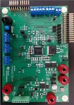
Figure 1. TPS99110EVM Board
E2E is a trademark of Texas Instruments.
Windows is a registered trademark of Microsoft Corporation.
All other trademarks are the property of their respective owners.
SLIU009 – February 2015
Submit Documentation Feedback
TPS99110EVM and GUI User's Guide
Copyright © 2015, Texas Instruments Incorporated
1
�Introduction
1.1
www.ti.com
Contents of EVM kit
The TPS9110EVM kit includes the following contents:
• Evaluation module board with a sample TPS99110-Q1 device
• USB connector
1.2
Related Documents from Texas Instruments
The following lists related documentation regarding TI's integrated circuits used in the assembly of the
TPS99110EVM. These documents are available on www.TI.com.
• TPS99110-Q1 System-Basis Chip for Automotive Applications, SLIS155
1.3
Equipment Needed for Evaluation
The following equipment is required for evaluation of the TPS99110-Q1 device:
• Power supply capable of 14-V, 2-A operation
• Personal computer (PC) with Windows® operating system (XP or later)
• Digital multimeter
• Oscilloscope
2
EVM Hardware
The TPS99110EVM is used to evaluate the TPS99110-Q1 device. The EVM board already includes a
TPS99110-Q1 device which eliminates the need for immediate soldering. Refer to the TPS9110-Q1
datasheet and Section 4 for more detail on the application configuration. The following function blocks are
accessible on the EVM hardware and are highlighted in Figure 1.
• Two adjustable sensor supplies
• CAN and LIN communication interfaces
• Two integrated operational amplifiers
• Three current-loop interfaces
• LDO regulator outputs
• All digital input and output signals
2
TPS99110EVM and GUI User's Guide
SLIU009 – February 2015
Submit Documentation Feedback
Copyright © 2015, Texas Instruments Incorporated
�EVM Hardware
www.ti.com
2.1
Initial Setup
To operate and evaluate the EVM properly, the following steps must be followed:
Step 1. Supplied the TPS99110EVM with power for basic operation. Connect the power supply
ground to the P1 banana jack, and connect the positive terminal of the power supply to the
P4 banana jack. For a description of the uses for the rest of the banana jacks, see Table 1.
Step 2. Populate the necessary jumpers (J26, J24, J25, J1, and J14) if these jumpers are not already
populated on the board for the proper power up.
Step 3. Position SW1 in the correct location if it is not already in the correct position. To ensure that
SW1 is positioned correctly, verify that it is switched to the 1-2 position (as shown in Figure
1).
Step 4. Connect the TIGER interface board to the J11 header as shown in Figure 2. For the GUI to
communicate with the TPS99110-Q1 device, this interface board must be connected and
jumpers J5, J7, J8, and J12 must be populated.
Step 5. Connect the TIGER interface board to the controlling PC using USB connector after the
TIGER interface board is connected and jumpers are populated.
Step 6. Set the voltage on the power supply. The VBAT (P4) port should be set for 12 V which is the
nominal voltage of the TPS99110-Q1 device.
CAUTION
The voltage can go up to a maximum of 38.5 V. Operating the device at a
voltage higher than the maximum for an extended amount of time will damage
the device.
Step 7.
Step 8.
Step 9.
Switch on the power supply to power up the EVM.
Open the TPS99110EVM GUI. To verify that the GUI initialized correctly, check the TIGER
status box which should display Firmware 1.3.6.
Begin evaluating the device.
Figure 2. TIGER Board Configuration
SLIU009 – February 2015
Submit Documentation Feedback
TPS99110EVM and GUI User's Guide
Copyright © 2015, Texas Instruments Incorporated
3
�EVM Hardware
2.2
www.ti.com
Banana Jacks
The TPS99110EVM has 5 banana jacks. These ports provide a convenient means to connect the EVM
board to external circuits or power supplies that may require high current. Table 1 lists all banana jacks
and corresponding functions.
Table 1. Banana Jack Descriptions
BANANA JACK DESIGNATOR
2.3
FUNCTION
P1
GND connection, best used for power supply
P2
If the user chooses, can be used to externally supply VIO
P3
If the user chooses, can be used to externally supply
SENSOR_IN
P4
Positive terminal of the board power supply
P5
If the user chooses, can be used to externally supply VOP
Jumpers
The TPS99110EVM has 16 jumpers that provide a simple way to configure signals to and from the
TPS99110-Q1 device on the board. Table 2 lists all jumpers and corresponding functions.
Table 2. Jumper Descriptions
JUMPER
4
JUMPER NAME
FUNCTION
J1
NWDDIS
Shorts the NWDDIS pin to GND, disabling the Watchdog for
evaluation.
J5
SDO
Connects the SDO pin to the TIGER interface board
J7
CLK
Connects the CLK pin to the TIGER interface board
J8
NCS
Connects the NCS pin to the TIGER interface board
J9
PRE2/PRE1 SNS
Shorts PRE1SNS and PRE2SNS together
J10
PWL_WD
Connects the PWL_WD pin to the TIGER interface board
J12
SDI
Connects the SDI pin to the TIGER interface board
J13
NRST3
Connects the NRST3 pin to the TIGER interface board
J14
VDD5_CAN
Supplies VDD5_CAN from the VDD5 regulator on the TPS99110-Q1
device
J15
NRST5
Connects the NRST5 pin to the TIGER interface board
J18
PWL_WD GND
Connects the PWL_WD pin to GND
J22
NWDDIS TIGER
Connects the NWDDIS pin to the TIGER interface board
J23
NResistorTART
Connects the NResistorTART pin to the TIGER interface board
J24
VIO supply
Position 1-2: Supplies VIO from the VDD5 regulator
Position 2-3: Supplies VIO from the VDD3 regulator
Leave unpopulated to use the P2 banana jack for VIO supply
J25
SENSOR_IN supply
Position 1-2: Supplies SENSOR_IN from the PRE1SNS pin
Position 2-3: Supplies SENSOR_IN from the PRE2SNS pin
Leave unpopulated to use the P3 banana jack for SENSOR_IN supply
J26
VOP supply
Position 1-2: Supplies VOP from the PRE1SNS pin
Position 2-3: Supplies VOP from the PRE2SNS pin
Leave unpopulated to use the P5 banana jack for VOP supply
TPS99110EVM and GUI User's Guide
SLIU009 – February 2015
Submit Documentation Feedback
Copyright © 2015, Texas Instruments Incorporated
�EVM Hardware
www.ti.com
2.4
Test Points
There are 5 test points scattered across the board, all connected to the board GND. These are just for the
convenience of the user when probing any point on the EVM.
3
GUI Software
The GUI software to go along with the TPS99110EVM is a simple, and coherent interface to control the
TPS99110-Q1 device. The GUI is divided into 2 different tabs: one for custom SPI commands the user
can input themselves, and one for the SPI register map.
3.1
SPI Command Tab
The SPI Command tab provides the user the option to write their own SPI commands or to read the
register of their choice. Figure 3 shows the SPI Command which includes dialog boxes for the register
address, the write data, the output data in hexadecimal, and the output data in binary. This tab also
includes two drop down menus; one for the read or write selection and one for the register space. The
register space will always be set to CAS. To send a command, the corresponding ENABLE button must
be clicked followed by the clicking SEND ALL button. The user can also enable multiple commands at one
time and then click the SEND ALL button to send multiple commands at once.
Figure 3. SPI Command Tab
SLIU009 – February 2015
Submit Documentation Feedback
TPS99110EVM and GUI User's Guide
Copyright © 2015, Texas Instruments Incorporated
5
�GUI Software
3.1.1
www.ti.com
Write Command
To use the write command, the user must first select Write from the Read/Write Menu drop-down. Then
the address (in hexadecimal) should be entered into the ADDR (HEX) dialog box. The data that is to be
written (in hexadecimal) to the selected register is then entered into the DATA IN dialog box. The ENABLE
button must then be clicked for the write to occur. When the write is complete, the DATA OUT (HEX)
dialog box and the DATA OUT dialog box should display the resulting write. If the DATA OUT dialog box
does not match what the was written, an issue with the TIGER interface board may have occurred. Click
the RECONNECT TIGER button next to the title of the GUI (see Figure 4). After clicking this button, try to
click the ENABLE button again and ensure that the data-out dialog boxes match what was written.
3.1.2
Read Command
To use the read command, the user must first select Read from the Read/Write Menu drop-down. Then
the address (in hexadecimal) should be entered into the ADDR (HEX) dialog box. The DATA IN box is left
blank. Click the ENABLE button for the read to occur. When the read is complete, the register data that
was read should be displayed in the DATA OUT (HEX) and DATA OUT dialog boxes.
3.2
SPI Register Map Tab
The SPI Register Map tab provides the user an easy-to-use interface to control every accessible register
and bit. Each bit has a title associated to provide some description of the bit. For the detailed bit
descriptions, refer to the TPS99110-Q1 data sheet. Each bit also has a box that shows the bit setting
(either a 0 or a 1) at any given read. The 0 setting appears with a red background and the 1 appears with
a green background.
Figure 4. SPI Register Map
6
TPS99110EVM and GUI User's Guide
SLIU009 – February 2015
Submit Documentation Feedback
Copyright © 2015, Texas Instruments Incorporated
�Schematic, Layout, and Bill of Materials
www.ti.com
3.2.1
Read Register Map
To read all the registers, click the READ CAS REGMAP button. Clicking this button also updates the
register map. If the map displays something that is not expected, try reconnecting the TIGER interface
board by clicking the RECONNECT TIGER button at the top of the GUI.
3.2.2
Write to Register Map
To write to register bits using the register, click the bit to flip the current setting. After the setting is
changed, click the WRITE CAS REGMAP button to write every change that has been implemented since
the last read or write.
3.2.3
Initialize Register Map
To populate the register map with default values, click the INITIALIZE CAS REGMAP. This feature is
helpful if the user has made numerous changes but wants to go back to the normal settings without power
cycling the EVM.
4
Schematic, Layout, and Bill of Materials
The following sections include the schematic, layout, and bill of materials (BOM) for the TPS99110EVM.
SLIU009 – February 2015
Submit Documentation Feedback
TPS99110EVM and GUI User's Guide
Copyright © 2015, Texas Instruments Incorporated
7
�Schematic, Layout, and Bill of Materials
4.1
www.ti.com
Schematic
R1
VDD5
NRST5
CLSS_OUT1
PRE1SNS
1µF
VIO
GND
P2
J9
IPD25N06S4L-30
Q2
5.5V - 38V
PRE2GATE
C11
0.1µF
C8
150pF
GND
47.0k
GND
VDD1GATE 32
VDD1ADJ
PRE2SNS
2
VDD5
31
VIO
28
VIN
17
VDD3
R12
CJS-1201TA
VDD1GATE
Q3
IPB081N06L3 G
GND
CLK
SDI
SDO
NCS
J18
3
1
R15
100k
SW2
VIN
VDD1
VIN
2
WAKE
8
7
OUT1
6
INP2
INN2
9
10
100k
61
38
R14
R16
R17
R18
499
499
499
499
36
34
35
33
PWL_WD
NWDDIS
4 WAKE
1
6
R19
2.49k
C16
4.7µF
R20
VDD1ADJ
GND
GND
VDD5
R23
10k
VDD3
C20
10µF
PRE1SNS
C21
10µF
VIN
1.0k
GND
GPBS-800L
J25
P3
INP1
INN1
ENA
WAKE
5
3
GND
12
OUT2 11
3
4
VIO
NENDRV
1.0k
GND
C19
0.1µF
30
54
NRESTART
NRST5
NRST3
ENDRV
NENDRV
45
51
53
26
25
CP
14
GND
CP2
16
CP1
15
SENSOR_IN
PRE2SNS
GND
C6
0.022µF
50V
GND
GND
GND
GND
GND
GND
GND
GND
SDO
J7
VDD5_CAN
VDD3
J14
GND
1
R11
CLSS_IN3 NWDDIS
C5
0.022µF
50V
CLK
43
SW1
VDD5
CLSS_IN2
C12
0.1µF
VIN
J24
C4
0.022µF
50V
J5
VDD5
VDD1GATE
VSOUT1
VSOUT2
VSOUT3
VDD1ADJ
VIO
TESTOUT1
TESTOUT2
BAT_OUT
VIN
KL
KL_TXD
KL_RXD
GND
GND
CLSS_IN1
U1
C14
0.1µF
10k
GND
J6
VOP
BAT_OUT
GND
VDD5_CAN
1µF
R8
R2
1.0k
C3
1µF
VDD5
C13
BAT_OUT_FILT
C9
150pF
VSOUT3
J1
PRE2SNS
R7
68k
R9
C2
1µF
GND
R5
100k
GND
VSOUT2
C1
1µF
C22
0.01µF
GND
VOP
OUT1
SPLIT
CAN_RXD
CAN_TXD
CAN_L
CAN_H
INP2
INN2
PRE1GATE
PRE1SNS
INP1
INN1
OUT2
SENSOR_IN
ENA
WAKE
PRE2GATE
PRE2SNS
CLK
SDI
SDO
NCS
DLY_RST
CLSS_IN1
CLSS_IN2
CLSS_IN3
PWL_WD
NWDDIS
CLSS_OUT1
CLSS_OUT2
CLSS_OUT3
NRESTART
NRST5
NRST3
ENDRV
NENDRV
REF_CL
GND
GND
GND
GND
GND
GND
GND_CAN
CP
CP1
CP2
DAP
29
VDD3
24
VDD5
J8
J10
NCS
PWL_WD
J11
57 VSOUT1
58 VSOUT2
59 VSOUT3
J13
R4
0
R6
56
19
18
BAT_OUT
49
48
47
KL
KL_TXD
KL_RXD
39
46
44
41
40
SPLIT
CAN_RXD
CAN_TXD
CAN_N
CAN_P
21
20
PRE1GATE
PRE1SNS
NRST3
GND
0
GND
J15
NRST5
KL
C15
1000pF
R10
1.0k
1
3
5
7
9
11
13
15
17
19
21
23
25
27
29
2
4
6
8
10
12
14
16
18
20
22
24
26
28
30
J12
SDI
J22
NWDDIS
J23
NRESTART
3
C10
VSOUT1
GND
BAS16W-7-F
75V
D1
J16
1
R3
100k
GND
J4
Vout (max)=5V; Iout (max)=100mA
Vout (max)=8.25V; Iout=200mA
Vout (max)=8.25V; Iout=200mA
J2
Vout=0.98V; Iout (max)=700mA
Vout=3.3V; Iout (max)=400mA
Vout=5V; Iout (max)=400mA
J3
PRE1GATE
NRST3
CLSS_OUT3
8
7
6
5
4
3
2
1
C7
150pF
IPD25N06S4L-30
Q1
P1
CLSS_OUT2
2.0k
OUT1
INP1
INN1
VSOUT1
VSOUT2
VSOUT3
VDD5
VDD3
VDD1
CLSS_IN1
CLSS_IN2
CLSS_IN3
VIN
OUT2
INP2
INN2
Figure 5 shows the schematic for the TPS99110EVM.
NENDRV
ENDRV
55 SENSOR_IN
VIN
23
22
PRE2GATE
PRE2SNS
52
DLY_RST
J17
KL
VIN
R13
22k
62 CLSS_IN1
63 CLSS_IN2
64 CLSS_IN3
GND
GND
KL_RXD
J19
2 CLSS_OUT1
3 CLSS_OUT2
4 CLSS_OUT3
5
4
3
2
1
C17
56pF
1 REF_CL
GND
C18
22pF
R22
2.4k
VDD5_CAN
SPLIT
CAN_N
CAN_P
GND
R21
10k
5
13
27
37
50
60
42
GND
GND
GND
J20
SDO
CLK
NCS
SDI
VIO
65
GND
TPS99110PAP
2 CAN_TXD
4 CAN_RXD
PWL_WD
6
WAKE
8
10 NRESTART
1
3
5
7
9
GND
J21
L1
D2
C27
0.1µF
ACT45B-510-2P-TL003
PDS560-13
GND
GND
GND
GND
C28
0.1µF
Q4
3
C29
4.7µF
R27
60.4
CAN_P
4
L2
1
4700pF
GND
Q5
CAN_N
R24
60.4
2,4
R28
1.0k
SPLIT
51µH
1
1
DNP D3
BZX384
C30
GND
IPD25N06S4L-30
4
J26
DNP
PRE1SNS
VOP
PRE2SNS
GND
100k
R26
3
R25
1.0k
P5
NRST3
2
NRST5
4
6 ENA
8 NWDDIS
10 BAT_OUT_FILT
1
3
5
7
9
2
C24
C26
47µF
0.082µF
C25
0.082µF
60V
3
P4
GND
VIN
KL_TXD
KL_RXD
CLSS_OUT1
CLSS_OUT2
CLSS_OUT3
C32
22pF
IHLP2020BZER4R7M11
D4
B360A-13-F
CAN_RXD
C31
56pF
GND
R29
10k
GND
GND
GND
GND
GND
GND
C23
22pF
CP
GND
GND
Figure 5. TPS99110EVM Schematic
8
TPS99110EVM and GUI User's Guide
SLIU009 – February 2015
Submit Documentation Feedback
Copyright © 2015, Texas Instruments Incorporated
�Schematic, Layout, and Bill of Materials
www.ti.com
4.2
Component Layout
Figure 6 and Figure 7 show the component layout for the PCB.
Components marked DNP should not be populated.
Figure 6. Top-Side Layer
Components marked DNP should not be populated.
Figure 7. Bottom-Side Layer
SLIU009 – February 2015
Submit Documentation Feedback
TPS99110EVM and GUI User's Guide
Copyright © 2015, Texas Instruments Incorporated
9
�Schematic, Layout, and Bill of Materials
4.3
www.ti.com
Bill of Materials
Table 3 lists the BOM for the TPS99110EVM.
Table 3. BOM
QUANTITY
PART NUMBER
MANUFACTURER
!PCB1
1
C1, C2, C3
3
1 µF
Capacitor, ceramic, 1 µF, 50 V, ±10%, X7R, 1206
1206
HVL096
Any
C3216X7R1H105K
C4, C5, C6
3
0.022 µF
Capacitor, ceramic, 0.022 µF, 50 V, ±10%, X8R, 0603
TDK
0603
C1608X8R1H223K
C7, C8, C9
3
150 pF
TDK
Capacitor, ceramic, 150 pF, 50 V, ±5%, C0G/NP0, 0805
0805
C0805C151J5GACTU
C10, C13
2
Kemet
1 µF
Capacitor, ceramic, 1 µF, 50 V, ±10%, X7R, 1206
1206
GRM31MR71H105KA88L
C11
MuRata
1
0.1 µF
Capacitor, ceramic, 0.1 µF, 50 V, ±10%, X7R, 0805
0805
C2012X7R1H104K
TDK
C12
1
0.1 µF
Capacitor, ceramic, 0.1 µF, 50 V, ±10%, X7R, 0805
0805
C0805C104K5RACTU
Kemet
C14
1
0.1 µF
Capacitor, ceramic, 0.1 µF, 50 V, ± 10%, X7R, 0805
0805
GRM21BR71H104KA01L
MuRata
C15
1
1000 pF
Capacitor, ceramic, 1000 pF, 50 V, ±5%, C0G/NP0, 0805
0805
GRM2165C1H102JA01D
MuRata
C16, C29
2
4.7 µF
Capacitor, ceramic, 4.7 µF, 50 V, ±10%, X5R, 1206
1206
GRM319R61H475KA12
MuRata
C17, C31
2
56 pF
Capacitor, ceramic, 56 pF, 50 V, ±5%, C0G/NP0, 0805
0805
C0805C560J5GACTU
Kemet
C18, C23, C32
3
22 pF
Capacitor, ceramic, 22 pF, 50 V, ±5%, C0G/NP0, 0805
0805
08055A220JAT2A
AVX
C19, C28
2
0.1 µF
Capacitor, ceramic, 0.1 µF, 50 V, ±5%, X7R, 0805
0805
08055C104JAT2A
AVX
C20, C21
2
10 µF
Capacitor, ceramic, 10 µF, 50 V, ±10%, X7R, 1210
1210
GRM32ER71H106KA12L
MuRata
C22
1
0.01 µF
Capacitor, ceramic, 0.01 µF, 50 V, ±5%, C0G/NP0, 0805
0805
GRM2195C1H103JA01D
MuRata
C24
1
47 µF
Capacitor, aluminum, 47 µF, 50 V, ± 20%, Ω, SMD
F80
EMVA500ADA470MF80G
Nippon Chemi-Con
C25, C26
2
0.082 µF
Capacitor, ceramic, 0.082 µF, 50 V, ± 10%, X7R, 0805
0805
08055C823KAT2A
AVX
C27
1
0.1 µF
Capacitor, ceramic, 0.1 µF, 50 V, ± 20%, X7R, 0805
0805
C0805C104M5RACTU
Kemet
C30
1
4700 pF
Capacitor, ceramic, 4700 pF, 50 V, ±5%, X7R, 0805
0805
08055C472JAT2A
AVX
D1
1
75 V
Diode, switching, 75 V, 0.15 A, SOT-323
SOT-323
BAS16W-7-F
Diodes Inc.
D2
1
60 V
Diode, Schottky, 60 V, 5A, PowerDI5
PowerDI5
PDS560-13
Diodes Inc.
D4
1
60 V
Diode, Schottky, 60 V, 3 A, SMA
SMA
B360A-13-F
Diodes Inc.
H1, H2, H3, H4
4
Machine screw, round, #4-40 × 1/4, nylon, Philips panhead
Screw
NY PMS 440 0025 PH
BXYZF Fastener Supply
H5, H6, H7, H8
4
Standoff, hex, 0.5"L #4-40 nylon
Standoff
1902C
Keystone
J1, J5, J7, J8, J9,
J10, J12, J13, J14,
J15, J18, J22, J23
13
Header, 100 mil, 2 × 1, tin, TH
Header, 2 × 1, 100 mil,
TH
5-146278-2
TE Connectivity
J2, J3, J4, J17
4
Terminal block, 6 A, 3.5 mm pitch, 3-Pos, TH
10.5 × 8.2 × 6.5 mm
ED555/3DS
On-Shore Technology
J6
1
Terminal block, 8 × 1, 2.54 mm, TH
8POS Terminal Block
1725711
Phoenix Contact
J11
1
R/A header, 100 mil, 15 × 2, gold, TH
15 × 2 R/A Header
PBC15DBAN
Sullins Connector Solutions
J16
1
Terminal block, 6 A, 3.5 mm pitch, 2-Pos, TH
7 × 8.2 × 6.5 mm
ED555/2DS
On-Shore Technology
J19
1
Terminal block, 6 A, 3.5 mm pitch, 5-Pos, TH
17.5 × 8.2 × 6.5mm
ED555/5DS
On-Shore Technology
Header, 100 mil, 5 × 2, gold, R/A, TH
Header, 5 × 2, 100 mil,
R/A
TSW-105-08-G-D-RA
Samtec
J20, J21
10
VALUE
PACKAGE
REFERENCE
DESIGNATOR
DESCRIPTION
Printed circuit board
2
TPS99110EVM and GUI User's Guide
SLIU009 – February 2015
Submit Documentation Feedback
Copyright © 2015, Texas Instruments Incorporated
�Schematic, Layout, and Bill of Materials
www.ti.com
Table 3. BOM (continued)
DESIGNATOR
QUANTITY
J24, J25, J26
3
L1
1
L2
1
DESCRIPTION
PACKAGE
REFERENCE
PART NUMBER
MANUFACTURER
Header, 100 mil, 3 × 1, Tin, TH
Header, 3 × 1, 100 mil,
TH
5-146278-3
TE Connectivity
4.7 µH
Inductor, shielded drum core, powdered iron, 4.7 µH, 3 A, 0.0813
Ω, SMD
5.49 × 2 × 5.18 mm
IHLP2020BZER4R7M11
Vishay-Dale
51 µH
Coupled inductor, 51 µH, 0.2 A, 1 Ω, SMD
4.5 × 2.8 × 3.2 mm
ACT45B-510-2P-TL003
TDK
SPC15354
Tenma
VALUE
P1
1
Banana jack, solder lug, black, TH
Black insulated banana
jack
P2, P3, P4, P5
4
Banana jack, solder lug, red, TH
Red insulated banana
jack
SPC15363
Tenma
Q1, Q2, Q4
3
60 V
MOSFET, N-CH, 60 V, 25 A, DPAK
DPAK
IPD25N06S4L-30
Infineon Technologies
Q3
1
60 V
MOSFET, N-CH, 60 V, 50 A, DDPAK
DDPAK
IPB081N06L3 G
Infineon Technologies
Q5
1
40 V
Transistor, NPN, 40 V, 0.6 A, SOT-89
SOT-89
DXT2222A-13
Diodes Inc.
R1
1
2 kΩ
Resistor, 2 kΩ, 5%, 0.125 W, 0805
0805
CRCW08052K00JNEA
Vishay-Dale
R2, R10, R11, R20
4
1 kΩ
Resistor, 1 kΩ, 5%, 0.125 W, 0805
0805
CRCW08051K00JNEA
Vishay-Dale
R3, R5, R15
3
100 kΩ
Resistor, 100 kΩ, 5%, 0.125 W, 0805
0805
CRCW0805100KJNEA
Vishay-Dale
R4, R6
2
0Ω
Resistor, 0 Ω, 5%, 0.125 W, 0805
0805
CRCW08050000Z0EA
Vishay-Dale
R7
1
68 kΩ
Resistor, 68 k, 5%, 0.125 W, 0805
0805
CRCW080568K0JNEA
Vishay-Dale
R8
1
47 kΩ
Resistor, 47 kΩ, 0.1%, 0.125 W, 0805
0805
RT0805BRD0747KL
Yageo America
R9
1
10 kΩ
Resistor, 10 kΩ, 5%, 0.125 W, 0805
0805
CRCW080510K0JNEA
Vishay-Dale
R12
1
100 kΩ
Resistor, 100 kΩ, 5%, 0.125 W, 0805
0805
ERJ-6GEYJ104V
Panasonic
R13
1
22 kΩ
Resistor, 22 kΩ, 5%, 0.125 W, 0805
0805
CRCW080522K0JNEA
Vishay-Dale
R14, R16, R17, R18
4
499 Ω
Resistor, 499 Ω, 1%, 0.1 W, 0603
0603
CRCW0603499RFKEA
Vishay-Dale
R19
1
2.49 kΩ
Resistor, 2.49 kΩ, 1%, 0.125 W, 0805
0805
CRCW08052K49FKEA
Vishay-Dale
R21, R23, R29
3
10 kΩ
Resistor, 10 kΩ, 5%, 0.125 W, 0805
0805
CRCW080510K0JNEA
Vishay-Dale
R22
1
2.4 kΩ
Resistor, 2.4 kΩ, 5%, 0.125 W, 0805
0805
CRCW08052K40JNEA
Vishay-Dale
R24, R27
2
60.4 Ω
Resistor, 60.4 Ω, 1%, 0.125 W, 0805
0805
CRCW080560R4FKEA
Vishay-Dale
R25, R28
2
1.0 kΩ
Resistor, 1 kΩ, 5%, 0.125 W, 0805
0805
CRCW08051K00JNEA
Vishay-Dale
SH-J1, SH-J2, SH-J3,
5
SH-J4, SH-J5
Shunt, 100 mil, Gold plated, Black
Shunt 2 pos. 100 mil
881545-2
TE Connectivity
SW1
1
Slide SW, SPDT 0.1 A 50 VDC
SW, 3.1 × 2.5 × 6 mm
CJS-1201TA
Copal Electronics
SW2
1
Switch, pushbutton, DPDT, TH
Switch, 8 × 13.5 × 8mm
GPBS-800L
CW Industries
Test point, multipurpose, black, TH
Black multipurpose
testpoint
5011
Keystone
TP1, TP2, TP3, TP4,
TP5, TP6
6
U1
1
System basis chip for automotive applications, PAP0064F
PAP0064F
TPS99110PAP
Texas Instruments
D3
0
Diode, Zener, 15 V, 300 mW, SOD-323
SOD-323
BZX384-C15,115
NXP Semiconductor
FID1, FID2, FID3
0
Fiducial mark. There is nothing to buy or mount.
Fiducial
—
—
FID4, FID5, FID6
0
Fiducial mark. There is nothing to buy or mount.
—
—
—
R26
0
Resistor, 100 kΩ, 5%, 0.125 W, 0805
0805
CRCW0805100KJNEA
Vishay-Dale
Black
100 kΩ
SLIU009 – February 2015
Submit Documentation Feedback
TPS99110EVM and GUI User's Guide
Copyright © 2015, Texas Instruments Incorporated
11
�STANDARD TERMS AND CONDITIONS FOR EVALUATION MODULES
1.
Delivery: TI delivers TI evaluation boards, kits, or modules, including any accompanying demonstration software, components, or
documentation (collectively, an “EVM” or “EVMs”) to the User (“User”) in accordance with the terms and conditions set forth herein.
Acceptance of the EVM is expressly subject to the following terms and conditions.
1.1 EVMs are intended solely for product or software developers for use in a research and development setting to facilitate feasibility
evaluation, experimentation, or scientific analysis of TI semiconductors products. EVMs have no direct function and are not
finished products. EVMs shall not be directly or indirectly assembled as a part or subassembly in any finished product. For
clarification, any software or software tools provided with the EVM (“Software”) shall not be subject to the terms and conditions
set forth herein but rather shall be subject to the applicable terms and conditions that accompany such Software
1.2 EVMs are not intended for consumer or household use. EVMs may not be sold, sublicensed, leased, rented, loaned, assigned,
or otherwise distributed for commercial purposes by Users, in whole or in part, or used in any finished product or production
system.
2
Limited Warranty and Related Remedies/Disclaimers:
2.1 These terms and conditions do not apply to Software. The warranty, if any, for Software is covered in the applicable Software
License Agreement.
2.2 TI warrants that the TI EVM will conform to TI's published specifications for ninety (90) days after the date TI delivers such EVM
to User. Notwithstanding the foregoing, TI shall not be liable for any defects that are caused by neglect, misuse or mistreatment
by an entity other than TI, including improper installation or testing, or for any EVMs that have been altered or modified in any
way by an entity other than TI. Moreover, TI shall not be liable for any defects that result from User's design, specifications or
instructions for such EVMs. Testing and other quality control techniques are used to the extent TI deems necessary or as
mandated by government requirements. TI does not test all parameters of each EVM.
2.3 If any EVM fails to conform to the warranty set forth above, TI's sole liability shall be at its option to repair or replace such EVM,
or credit User's account for such EVM. TI's liability under this warranty shall be limited to EVMs that are returned during the
warranty period to the address designated by TI and that are determined by TI not to conform to such warranty. If TI elects to
repair or replace such EVM, TI shall have a reasonable time to repair such EVM or provide replacements. Repaired EVMs shall
be warranted for the remainder of the original warranty period. Replaced EVMs shall be warranted for a new full ninety (90) day
warranty period.
3
Regulatory Notices:
3.1 United States
3.1.1
Notice applicable to EVMs not FCC-Approved:
This kit is designed to allow product developers to evaluate electronic components, circuitry, or software associated with the kit
to determine whether to incorporate such items in a finished product and software developers to write software applications for
use with the end product. This kit is not a finished product and when assembled may not be resold or otherwise marketed unless
all required FCC equipment authorizations are first obtained. Operation is subject to the condition that this product not cause
harmful interference to licensed radio stations and that this product accept harmful interference. Unless the assembled kit is
designed to operate under part 15, part 18 or part 95 of this chapter, the operator of the kit must operate under the authority of
an FCC license holder or must secure an experimental authorization under part 5 of this chapter.
3.1.2
For EVMs annotated as FCC – FEDERAL COMMUNICATIONS COMMISSION Part 15 Compliant:
CAUTION
This device complies with part 15 of the FCC Rules. Operation is subject to the following two conditions: (1) This device may not
cause harmful interference, and (2) this device must accept any interference received, including interference that may cause
undesired operation.
Changes or modifications not expressly approved by the party responsible for compliance could void the user's authority to
operate the equipment.
FCC Interference Statement for Class A EVM devices
NOTE: This equipment has been tested and found to comply with the limits for a Class A digital device, pursuant to part 15 of
the FCC Rules. These limits are designed to provide reasonable protection against harmful interference when the equipment is
operated in a commercial environment. This equipment generates, uses, and can radiate radio frequency energy and, if not
installed and used in accordance with the instruction manual, may cause harmful interference to radio communications.
Operation of this equipment in a residential area is likely to cause harmful interference in which case the user will be required to
correct the interference at his own expense.
SPACER
SPACER
SPACER
SPACER
SPACER
SPACER
SPACER
SPACER
�FCC Interference Statement for Class B EVM devices
NOTE: This equipment has been tested and found to comply with the limits for a Class B digital device, pursuant to part 15 of
the FCC Rules. These limits are designed to provide reasonable protection against harmful interference in a residential
installation. This equipment generates, uses and can radiate radio frequency energy and, if not installed and used in accordance
with the instructions, may cause harmful interference to radio communications. However, there is no guarantee that interference
will not occur in a particular installation. If this equipment does cause harmful interference to radio or television reception, which
can be determined by turning the equipment off and on, the user is encouraged to try to correct the interference by one or more
of the following measures:
•
•
•
•
Reorient or relocate the receiving antenna.
Increase the separation between the equipment and receiver.
Connect the equipment into an outlet on a circuit different from that to which the receiver is connected.
Consult the dealer or an experienced radio/TV technician for help.
3.2 Canada
3.2.1
For EVMs issued with an Industry Canada Certificate of Conformance to RSS-210
Concerning EVMs Including Radio Transmitters:
This device complies with Industry Canada license-exempt RSS standard(s). Operation is subject to the following two conditions:
(1) this device may not cause interference, and (2) this device must accept any interference, including interference that may
cause undesired operation of the device.
Concernant les EVMs avec appareils radio:
Le présent appareil est conforme aux CNR d'Industrie Canada applicables aux appareils radio exempts de licence. L'exploitation
est autorisée aux deux conditions suivantes: (1) l'appareil ne doit pas produire de brouillage, et (2) l'utilisateur de l'appareil doit
accepter tout brouillage radioélectrique subi, même si le brouillage est susceptible d'en compromettre le fonctionnement.
Concerning EVMs Including Detachable Antennas:
Under Industry Canada regulations, this radio transmitter may only operate using an antenna of a type and maximum (or lesser)
gain approved for the transmitter by Industry Canada. To reduce potential radio interference to other users, the antenna type
and its gain should be so chosen that the equivalent isotropically radiated power (e.i.r.p.) is not more than that necessary for
successful communication. This radio transmitter has been approved by Industry Canada to operate with the antenna types
listed in the user guide with the maximum permissible gain and required antenna impedance for each antenna type indicated.
Antenna types not included in this list, having a gain greater than the maximum gain indicated for that type, are strictly prohibited
for use with this device.
Concernant les EVMs avec antennes détachables
Conformément à la réglementation d'Industrie Canada, le présent émetteur radio peut fonctionner avec une antenne d'un type et
d'un gain maximal (ou inférieur) approuvé pour l'émetteur par Industrie Canada. Dans le but de réduire les risques de brouillage
radioélectrique à l'intention des autres utilisateurs, il faut choisir le type d'antenne et son gain de sorte que la puissance isotrope
rayonnée équivalente (p.i.r.e.) ne dépasse pas l'intensité nécessaire à l'établissement d'une communication satisfaisante. Le
présent émetteur radio a été approuvé par Industrie Canada pour fonctionner avec les types d'antenne énumérés dans le
manuel d’usage et ayant un gain admissible maximal et l'impédance requise pour chaque type d'antenne. Les types d'antenne
non inclus dans cette liste, ou dont le gain est supérieur au gain maximal indiqué, sont strictement interdits pour l'exploitation de
l'émetteur
3.3 Japan
3.3.1
Notice for EVMs delivered in Japan: Please see http://www.tij.co.jp/lsds/ti_ja/general/eStore/notice_01.page 日本国内に
輸入される評価用キット、ボードについては、次のところをご覧ください。
http://www.tij.co.jp/lsds/ti_ja/general/eStore/notice_01.page
3.3.2
Notice for Users of EVMs Considered “Radio Frequency Products” in Japan: EVMs entering Japan are NOT certified by
TI as conforming to Technical Regulations of Radio Law of Japan.
If User uses EVMs in Japan, User is required by Radio Law of Japan to follow the instructions below with respect to EVMs:
1.
2.
3.
Use EVMs in a shielded room or any other test facility as defined in the notification #173 issued by Ministry of Internal
Affairs and Communications on March 28, 2006, based on Sub-section 1.1 of Article 6 of the Ministry’s Rule for
Enforcement of Radio Law of Japan,
Use EVMs only after User obtains the license of Test Radio Station as provided in Radio Law of Japan with respect to
EVMs, or
Use of EVMs only after User obtains the Technical Regulations Conformity Certification as provided in Radio Law of Japan
with respect to EVMs. Also, do not transfer EVMs, unless User gives the same notice above to the transferee. Please note
that if User does not follow the instructions above, User will be subject to penalties of Radio Law of Japan.
SPACER
SPACER
SPACER
SPACER
SPACER
�【無線電波を送信する製品の開発キットをお使いになる際の注意事項】
本開発キットは技術基準適合証明を受けておりません。
本製品のご使用に際しては、電波法遵守のため、以下のいずれかの措置を取っていただく必要がありますのでご注意ください。
1.
2.
3.
電波法施行規則第6条第1項第1号に基づく平成18年3月28日総務省告示第173号で定められた電波暗室等の試験設備でご使用
いただく。
実験局の免許を取得後ご使用いただく。
技術基準適合証明を取得後ご使用いただく。
なお、本製品は、上記の「ご使用にあたっての注意」を譲渡先、移転先に通知しない限り、譲渡、移転できないものとします。
上記を遵守頂けない場合は、電波法の罰則が適用される可能性があることをご留意ください。
日本テキサス・インスツルメンツ株式会社
東京都新宿区西新宿6丁目24番1号
西新宿三井ビル
3.3.3
Notice for EVMs for Power Line Communication: Please see http://www.tij.co.jp/lsds/ti_ja/general/eStore/notice_02.page
電力線搬送波通信についての開発キットをお使いになる際の注意事項については、次のところをご覧くださ
い。http://www.tij.co.jp/lsds/ti_ja/general/eStore/notice_02.page
SPACER
4
EVM Use Restrictions and Warnings:
4.1 EVMS ARE NOT FOR USE IN FUNCTIONAL SAFETY AND/OR SAFETY CRITICAL EVALUATIONS, INCLUDING BUT NOT
LIMITED TO EVALUATIONS OF LIFE SUPPORT APPLICATIONS.
4.2 User must read and apply the user guide and other available documentation provided by TI regarding the EVM prior to handling
or using the EVM, including without limitation any warning or restriction notices. The notices contain important safety information
related to, for example, temperatures and voltages.
4.3 Safety-Related Warnings and Restrictions:
4.3.1
User shall operate the EVM within TI’s recommended specifications and environmental considerations stated in the user
guide, other available documentation provided by TI, and any other applicable requirements and employ reasonable and
customary safeguards. Exceeding the specified performance ratings and specifications (including but not limited to input
and output voltage, current, power, and environmental ranges) for the EVM may cause personal injury or death, or
property damage. If there are questions concerning performance ratings and specifications, User should contact a TI
field representative prior to connecting interface electronics including input power and intended loads. Any loads applied
outside of the specified output range may also result in unintended and/or inaccurate operation and/or possible
permanent damage to the EVM and/or interface electronics. Please consult the EVM user guide prior to connecting any
load to the EVM output. If there is uncertainty as to the load specification, please contact a TI field representative.
During normal operation, even with the inputs and outputs kept within the specified allowable ranges, some circuit
components may have elevated case temperatures. These components include but are not limited to linear regulators,
switching transistors, pass transistors, current sense resistors, and heat sinks, which can be identified using the
information in the associated documentation. When working with the EVM, please be aware that the EVM may become
very warm.
4.3.2
EVMs are intended solely for use by technically qualified, professional electronics experts who are familiar with the
dangers and application risks associated with handling electrical mechanical components, systems, and subsystems.
User assumes all responsibility and liability for proper and safe handling and use of the EVM by User or its employees,
affiliates, contractors or designees. User assumes all responsibility and liability to ensure that any interfaces (electronic
and/or mechanical) between the EVM and any human body are designed with suitable isolation and means to safely
limit accessible leakage currents to minimize the risk of electrical shock hazard. User assumes all responsibility and
liability for any improper or unsafe handling or use of the EVM by User or its employees, affiliates, contractors or
designees.
4.4 User assumes all responsibility and liability to determine whether the EVM is subject to any applicable international, federal,
state, or local laws and regulations related to User’s handling and use of the EVM and, if applicable, User assumes all
responsibility and liability for compliance in all respects with such laws and regulations. User assumes all responsibility and
liability for proper disposal and recycling of the EVM consistent with all applicable international, federal, state, and local
requirements.
5.
Accuracy of Information: To the extent TI provides information on the availability and function of EVMs, TI attempts to be as accurate
as possible. However, TI does not warrant the accuracy of EVM descriptions, EVM availability or other information on its websites as
accurate, complete, reliable, current, or error-free.
SPACER
SPACER
SPACER
SPACER
SPACER
SPACER
�SPACER
6.
Disclaimers:
6.1 EXCEPT AS SET FORTH ABOVE, EVMS AND ANY WRITTEN DESIGN MATERIALS PROVIDED WITH THE EVM (AND THE
DESIGN OF THE EVM ITSELF) ARE PROVIDED "AS IS" AND "WITH ALL FAULTS." TI DISCLAIMS ALL OTHER
WARRANTIES, EXPRESS OR IMPLIED, REGARDING SUCH ITEMS, INCLUDING BUT NOT LIMITED TO ANY IMPLIED
WARRANTIES OF MERCHANTABILITY OR FITNESS FOR A PARTICULAR PURPOSE OR NON-INFRINGEMENT OF ANY
THIRD PARTY PATENTS, COPYRIGHTS, TRADE SECRETS OR OTHER INTELLECTUAL PROPERTY RIGHTS.
6.2 EXCEPT FOR THE LIMITED RIGHT TO USE THE EVM SET FORTH HEREIN, NOTHING IN THESE TERMS AND
CONDITIONS SHALL BE CONSTRUED AS GRANTING OR CONFERRING ANY RIGHTS BY LICENSE, PATENT, OR ANY
OTHER INDUSTRIAL OR INTELLECTUAL PROPERTY RIGHT OF TI, ITS SUPPLIERS/LICENSORS OR ANY OTHER THIRD
PARTY, TO USE THE EVM IN ANY FINISHED END-USER OR READY-TO-USE FINAL PRODUCT, OR FOR ANY
INVENTION, DISCOVERY OR IMPROVEMENT MADE, CONCEIVED OR ACQUIRED PRIOR TO OR AFTER DELIVERY OF
THE EVM.
7.
USER'S INDEMNITY OBLIGATIONS AND REPRESENTATIONS. USER WILL DEFEND, INDEMNIFY AND HOLD TI, ITS
LICENSORS AND THEIR REPRESENTATIVES HARMLESS FROM AND AGAINST ANY AND ALL CLAIMS, DAMAGES, LOSSES,
EXPENSES, COSTS AND LIABILITIES (COLLECTIVELY, "CLAIMS") ARISING OUT OF OR IN CONNECTION WITH ANY
HANDLING OR USE OF THE EVM THAT IS NOT IN ACCORDANCE WITH THESE TERMS AND CONDITIONS. THIS OBLIGATION
SHALL APPLY WHETHER CLAIMS ARISE UNDER STATUTE, REGULATION, OR THE LAW OF TORT, CONTRACT OR ANY
OTHER LEGAL THEORY, AND EVEN IF THE EVM FAILS TO PERFORM AS DESCRIBED OR EXPECTED.
8.
Limitations on Damages and Liability:
8.1 General Limitations. IN NO EVENT SHALL TI BE LIABLE FOR ANY SPECIAL, COLLATERAL, INDIRECT, PUNITIVE,
INCIDENTAL, CONSEQUENTIAL, OR EXEMPLARY DAMAGES IN CONNECTION WITH OR ARISING OUT OF THESE
TERMS ANDCONDITIONS OR THE USE OF THE EVMS PROVIDED HEREUNDER, REGARDLESS OF WHETHER TI HAS
BEEN ADVISED OF THE POSSIBILITY OF SUCH DAMAGES. EXCLUDED DAMAGES INCLUDE, BUT ARE NOT LIMITED
TO, COST OF REMOVAL OR REINSTALLATION, ANCILLARY COSTS TO THE PROCUREMENT OF SUBSTITUTE GOODS
OR SERVICES, RETESTING, OUTSIDE COMPUTER TIME, LABOR COSTS, LOSS OF GOODWILL, LOSS OF PROFITS,
LOSS OF SAVINGS, LOSS OF USE, LOSS OF DATA, OR BUSINESS INTERRUPTION. NO CLAIM, SUIT OR ACTION SHALL
BE BROUGHT AGAINST TI MORE THAN ONE YEAR AFTER THE RELATED CAUSE OF ACTION HAS OCCURRED.
8.2 Specific Limitations. IN NO EVENT SHALL TI'S AGGREGATE LIABILITY FROM ANY WARRANTY OR OTHER OBLIGATION
ARISING OUT OF OR IN CONNECTION WITH THESE TERMS AND CONDITIONS, OR ANY USE OF ANY TI EVM
PROVIDED HEREUNDER, EXCEED THE TOTAL AMOUNT PAID TO TI FOR THE PARTICULAR UNITS SOLD UNDER
THESE TERMS AND CONDITIONS WITH RESPECT TO WHICH LOSSES OR DAMAGES ARE CLAIMED. THE EXISTENCE
OF MORE THAN ONE CLAIM AGAINST THE PARTICULAR UNITS SOLD TO USER UNDER THESE TERMS AND
CONDITIONS SHALL NOT ENLARGE OR EXTEND THIS LIMIT.
9.
Return Policy. Except as otherwise provided, TI does not offer any refunds, returns, or exchanges. Furthermore, no return of EVM(s)
will be accepted if the package has been opened and no return of the EVM(s) will be accepted if they are damaged or otherwise not in
a resalable condition. If User feels it has been incorrectly charged for the EVM(s) it ordered or that delivery violates the applicable
order, User should contact TI. All refunds will be made in full within thirty (30) working days from the return of the components(s),
excluding any postage or packaging costs.
10. Governing Law: These terms and conditions shall be governed by and interpreted in accordance with the laws of the State of Texas,
without reference to conflict-of-laws principles. User agrees that non-exclusive jurisdiction for any dispute arising out of or relating to
these terms and conditions lies within courts located in the State of Texas and consents to venue in Dallas County, Texas.
Notwithstanding the foregoing, any judgment may be enforced in any United States or foreign court, and TI may seek injunctive relief
in any United States or foreign court.
Mailing Address: Texas Instruments, Post Office Box 655303, Dallas, Texas 75265
Copyright © 2015, Texas Instruments Incorporated
spacer
�IMPORTANT NOTICE
Texas Instruments Incorporated and its subsidiaries (TI) reserve the right to make corrections, enhancements, improvements and other
changes to its semiconductor products and services per JESD46, latest issue, and to discontinue any product or service per JESD48, latest
issue. Buyers should obtain the latest relevant information before placing orders and should verify that such information is current and
complete. All semiconductor products (also referred to herein as “components”) are sold subject to TI’s terms and conditions of sale
supplied at the time of order acknowledgment.
TI warrants performance of its components to the specifications applicable at the time of sale, in accordance with the warranty in TI’s terms
and conditions of sale of semiconductor products. Testing and other quality control techniques are used to the extent TI deems necessary
to support this warranty. Except where mandated by applicable law, testing of all parameters of each component is not necessarily
performed.
TI assumes no liability for applications assistance or the design of Buyers’ products. Buyers are responsible for their products and
applications using TI components. To minimize the risks associated with Buyers’ products and applications, Buyers should provide
adequate design and operating safeguards.
TI does not warrant or represent that any license, either express or implied, is granted under any patent right, copyright, mask work right, or
other intellectual property right relating to any combination, machine, or process in which TI components or services are used. Information
published by TI regarding third-party products or services does not constitute a license to use such products or services or a warranty or
endorsement thereof. Use of such information may require a license from a third party under the patents or other intellectual property of the
third party, or a license from TI under the patents or other intellectual property of TI.
Reproduction of significant portions of TI information in TI data books or data sheets is permissible only if reproduction is without alteration
and is accompanied by all associated warranties, conditions, limitations, and notices. TI is not responsible or liable for such altered
documentation. Information of third parties may be subject to additional restrictions.
Resale of TI components or services with statements different from or beyond the parameters stated by TI for that component or service
voids all express and any implied warranties for the associated TI component or service and is an unfair and deceptive business practice.
TI is not responsible or liable for any such statements.
Buyer acknowledges and agrees that it is solely responsible for compliance with all legal, regulatory and safety-related requirements
concerning its products, and any use of TI components in its applications, notwithstanding any applications-related information or support
that may be provided by TI. Buyer represents and agrees that it has all the necessary expertise to create and implement safeguards which
anticipate dangerous consequences of failures, monitor failures and their consequences, lessen the likelihood of failures that might cause
harm and take appropriate remedial actions. Buyer will fully indemnify TI and its representatives against any damages arising out of the use
of any TI components in safety-critical applications.
In some cases, TI components may be promoted specifically to facilitate safety-related applications. With such components, TI’s goal is to
help enable customers to design and create their own end-product solutions that meet applicable functional safety standards and
requirements. Nonetheless, such components are subject to these terms.
No TI components are authorized for use in FDA Class III (or similar life-critical medical equipment) unless authorized officers of the parties
have executed a special agreement specifically governing such use.
Only those TI components which TI has specifically designated as military grade or “enhanced plastic” are designed and intended for use in
military/aerospace applications or environments. Buyer acknowledges and agrees that any military or aerospace use of TI components
which have not been so designated is solely at the Buyer's risk, and that Buyer is solely responsible for compliance with all legal and
regulatory requirements in connection with such use.
TI has specifically designated certain components as meeting ISO/TS16949 requirements, mainly for automotive use. In any case of use of
non-designated products, TI will not be responsible for any failure to meet ISO/TS16949.
Products
Applications
Audio
www.ti.com/audio
Automotive and Transportation
www.ti.com/automotive
Amplifiers
amplifier.ti.com
Communications and Telecom
www.ti.com/communications
Data Converters
dataconverter.ti.com
Computers and Peripherals
www.ti.com/computers
DLP® Products
www.dlp.com
Consumer Electronics
www.ti.com/consumer-apps
DSP
dsp.ti.com
Energy and Lighting
www.ti.com/energy
Clocks and Timers
www.ti.com/clocks
Industrial
www.ti.com/industrial
Interface
interface.ti.com
Medical
www.ti.com/medical
Logic
logic.ti.com
Security
www.ti.com/security
Power Mgmt
power.ti.com
Space, Avionics and Defense
www.ti.com/space-avionics-defense
Microcontrollers
microcontroller.ti.com
Video and Imaging
www.ti.com/video
RFID
www.ti-rfid.com
OMAP Applications Processors
www.ti.com/omap
TI E2E Community
e2e.ti.com
Wireless Connectivity
www.ti.com/wirelessconnectivity
Mailing Address: Texas Instruments, Post Office Box 655303, Dallas, Texas 75265
Copyright © 2015, Texas Instruments Incorporated
�