www.ti.com
Table of Contents
User’s Guide
TPSM84A21 and TPSM84A22 Power Module Evaluation
Module User's Guide
ABSTRACT
This user’s guide contains information for the TPSM84A21EVM-808 and TPSM84A22EVM-809 evaluation
modules (PWR808 and PWR809). This user's guide also includes the performance specifications, schematic, bill
of materials, and layout of the EVMs.
Table of Contents
1 Description.............................................................................................................................................................................. 2
2 Getting Started........................................................................................................................................................................2
3 Test Point Descriptions.......................................................................................................................................................... 4
4 Operation Notes......................................................................................................................................................................5
5 Performance Data................................................................................................................................................................... 6
6 Schematic................................................................................................................................................................................7
7 Bill of Material......................................................................................................................................................................... 8
8 PCB Layout..............................................................................................................................................................................9
9 Revision History....................................................................................................................................................................11
List of Figures
Figure 2-1. EVM User Interface................................................................................................................................................... 2
Figure 5-1. TPSM84A22EVM Efficiency (VG = OPEN)............................................................................................................... 6
Figure 5-2. TPSM84A22EVM Efficiency (VG = 5 V)....................................................................................................................6
Figure 5-3. TPSM84A22EVM Power Dissipation........................................................................................................................ 6
Figure 5-4. TPSM84A22EVM Output Voltage Ripple.................................................................................................................. 6
Figure 5-5. Output Current Transient Waveforms........................................................................................................................6
Figure 5-6. Output Current Transient Waveforms........................................................................................................................6
Figure 6-1. TPSM84A21EVM Schematic.................................................................................................................................... 7
Figure 8-1. Topside Component Layout.......................................................................................................................................9
Figure 8-2. Bottom-Side Component Layout............................................................................................................................... 9
Figure 8-3. Top Copper..............................................................................................................................................................10
Figure 8-4. Layer 2 Copper........................................................................................................................................................10
Figure 8-5. Layer 3 Copper........................................................................................................................................................ 11
Figure 8-6. Bottom Copper.........................................................................................................................................................11
List of Tables
Table 1-1. Output Voltage Range.................................................................................................................................................2
Table 3-1. Test Point Descriptions............................................................................................................................................... 4
Table 7-1. Bill of Material............................................................................................................................................................. 8
Trademarks
All trademarks are the property of their respective owners.
SLVUAT2A – NOVEMBER 2016 – REVISED FEBRUARY 2022
TPSM84A21 and TPSM84A22 Power Module Evaluation Module User's Guide
Submit Document Feedback
Copyright © 2022 Texas Instruments Incorporated
1
�Description
www.ti.com
1 Description
The TPSM84A21 and TPSM84A22 are synchronous buck power modules designed to provide up to 10 A of
output current. The TPSM84A21 and TPSM84A22 power modules combine the TPS54A20, a 10-A DC/DC
synchronous series capacitor buck converter with power MOSFETs, shielded inductors, input and output
capacitors, and passive components into a low-profile package. The input voltage range of both devices is 8
V to 14 V. See the Minimum Input Voltage curve in the TPSM84A22, 8-V to 14-V Input, 1.2-V to 2.05-V Output,
10-A SWIFT Power Module Data Sheet for the minimum required input voltage for VOUT > 1.5 V. The output
voltage ranges of both devices are given in Table 1-1. The output voltage of the EVM can be set to one of five
popular values by using a configuration jumper.
This evaluation module is designed to demonstrate the ease-of-use and small printed-circuit board (PCB) area
possible when designing with the TPSM84A21 and TPSM84A22 power modules. Monitoring test points are
provided to allow measurement of the following:
•
•
•
•
•
•
Efficiency
Power dissipation
Input ripple
Output ripple
Line and load regulation
Transient response
Additionally, control test points are provided for use of the power good, inhibit control, and undervoltage lockout
features of the device. The EVM uses a recommended PCB layout that maximizes thermal performance and
minimizes output ripple and noise.
Table 1-1. Output Voltage Range
EVM
Output Voltage Range
TPSM84A21EVM-808
0.55 V to 1.3 V
TPSM84A22EVM-809
1.2 V to 2.05 V
2 Getting Started
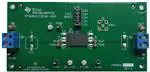
Figure 2-1 highlights the user interface items associated with the EVM. The polarized VIN power terminal block
(TB1) is used for connection to the host input supply and the polarized VOUT power terminal block (TB2) is used
for connection to the load. These terminal blocks can accept up to 16-AWG wire.
Figure 2-1. EVM User Interface
2
TPSM84A21 and TPSM84A22 Power Module Evaluation Module User's Guide
SLVUAT2A – NOVEMBER 2016 – REVISED FEBRUARY 2022
Submit Document Feedback
Copyright © 2022 Texas Instruments Incorporated
�www.ti.com
Getting Started
The VIN monitor and VOUT monitor test points located near the power terminal blocks are intended to be used
as voltage monitoring points where voltmeters can be connected to measure VIN and VOUT. The voltmeter
references should be connected to the PGND test points located beneath the power terminal blocks. Do not use
these VIN and VOUT monitoring test points as the input supply or output load connection points. The PCB traces
connecting to these test points are not designed to support high currents.
The VIN scope (J1) and VOUT scope (J2) test points can be used to monitor VIN and VOUT waveforms with an
oscilloscope. These test points are intended for use with un-hooded scope probes outfitted with a low-inductance
ground lead (ground spring) mounted to the scope barrel. The two sockets of each test point are on 0.1-inch
centers. The scope probe tip should be connected to the socket labeled VIN or VOUT, and the scope ground
lead should be connected to the socket labeled PGND.
The test points located directly below the device are made available to test the features of the device. Any
external connections made to these test points should be referenced to one of the PGND test points located
along the bottom of the EVM. Refer to Section 3 for more information on the individual control test points.
The VOUT SELECT jumper (P1) is provided for selecting the desired output voltage. Before applying power to
the EVM, ensure that the jumper is present and properly positioned for the intended output voltage.
SLVUAT2A – NOVEMBER 2016 – REVISED FEBRUARY 2022
TPSM84A21 and TPSM84A22 Power Module Evaluation Module User's Guide
Submit Document Feedback
Copyright © 2022 Texas Instruments Incorporated
3
�Test Point Descriptions
www.ti.com
3 Test Point Descriptions
Wire-loop test points and scope probe test points are provided as convenient connection points for digital
voltmeters (DVM) or oscilloscope probes to aid in the evaluation of the device. A BNC connector footprint (J3) is
available if a synchronization clock is required. Table 3-1 lists a description of each test point.
Table 3-1. Test Point Descriptions
Pin
Description
VIN
Input voltage monitor. Connect DVM to this point for measuring efficiency.
VOUT
Output voltage monitor. Connect DVM to this point for measuring efficiency, line regulation, and load regulation.
PGND
Input and output voltage monitor grounds. Reference the previously mentioned DVMs to any of these four analog
ground points.
VIN Scope (J1)
Input voltage scope monitor. Connect an oscilloscope to this set of points to measure input ripple voltage.
VOUT Scope (J2)
Output voltage scope monitor. Connect an oscilloscope to this set of points to measure output ripple voltage and
transient response.
EN/UVLO
Connect this point to control ground to disable the device. Allow this point to float to enable the device. An external
resistor divider can be connected between this point, control ground, and VIN to adjust the undervoltage lockout of
the device.
PGOOD
Monitors the power good signal of the device. This is an open-drain signal that requires an external pullup resistor if
monitoring is desired. A 10- to 100-kΩ pullup resistor is recommended. PWRGD is high if the output voltage is within
95% to 105% of its nominal value.
SYNC (J3)
Connects to the RT/CLK pin of the device. An external clock signal can be applied to this point to synchronize the
device to an appropriate frequency.
VG
Gate driver supply pin. If supplying an external 5-V supply, connect to this test point.
Note
Refer to the appropriate product data sheet for absolute maximum ratings associated with the
previously-listed features:
• TPSM84A21, 8V to 14V Input, 0.55V to 1.35V Output, 10-A SWIFT Power Module data sheet
• TPSM84A22, 8V to 14V Input, 1.2V to 2.05V Output, 10-A SWIFT Power Module data sheet
4
TPSM84A21 and TPSM84A22 Power Module Evaluation Module User's Guide
SLVUAT2A – NOVEMBER 2016 – REVISED FEBRUARY 2022
Submit Document Feedback
Copyright © 2022 Texas Instruments Incorporated
�www.ti.com
Operation Notes
4 Operation Notes
In order to operate the EVM, the input voltage must increase above the UVLO threshold of the device. The
UVLO threshold of the EVM is approximately 7.65 V with 200 mV of hysteresis. To adjust the UVLO threshold
to a higher voltage, the values of R8 and R9 on the EVM can be adjusted as described in the product data
sheet. The maximum operating input voltage for the device is 14 V. Refer to the product data sheet for further
information on the input voltage range and UVLO operation.
The minimum input voltage for the TPSM84A22 is 8 V or (VOUT × 5.3), whichever is greater.
The soft-start time is a fixed value and cannot be adjusted. After application of the proper input voltage, the
output voltage of the device will ramp to its final value in approximately 4.1 ms.
The power-good (PGOOD) indicator of the EVM will assert high when the output voltage is within ±5% of the
programmed output voltage value. A 100-kΩ pullup resistor (R11) is populated between the PGOOD pin and the
VG pin. The voltage on the VG pin is 4.8 V (typical). The VG and corresponding PGND test points are not loaded
on the EVM. If driving the VG pin is required, test points can be added to the EVM.
The current limit of the device can be set to 11.25 A (typical) by placing a 47-kΩ resistor between ILIM and
PGND. The EVM has a footprint for this resistor, R10, if needed.
The TPSM84A21 and TPSM84A22 nominal switching frequency is 4 MHz with a range of 3.7 MHz to 4.3 MHz
when free-running. If an exact switching frequency is required, both devices can be synchronized to an external
clock over the frequency range of 3.6 MHz to 4.4 MHz. Refer to the product data sheet for further information on
synchronization.
The TPSM84A21 and TPSM84A22 both include input and output capacitors internal to the device. For most
applications, no additional output capacitors are required. The EVM includes footprints for adding input and
output capacitors to the EVM. Adding additional capacitance will improve transient response. The actual
capacitance required will depend on the input and output voltage conditions of the particular application, along
with the desired transient response. Refer to the product data sheet for further information on input and output
capacitance and transient response.
SLVUAT2A – NOVEMBER 2016 – REVISED FEBRUARY 2022
TPSM84A21 and TPSM84A22 Power Module Evaluation Module User's Guide
Submit Document Feedback
Copyright © 2022 Texas Instruments Incorporated
5
�Performance Data
www.ti.com
5 Performance Data
The graphs and waveforms in Figure 5-1 to Figure 5-6 demonstrate the performance of the TPSM84A22EVM.
100
12
80
70
10
Efficiency (%)
Minimum Input Voltage (V)
90
11
9
8
50
40
30
6
1.2
VOUT
2.05 V
1.8 V
1.5 V
1.2 V
20
TA
85°C
25°C
7
10
0
1.3
1.4
1.5
1.6
1.7
1.8
Output Voltage (V)
1.9
2.0
0
2.1
1
2
3
4
D007
Figure 5-1. TPSM84A22EVM Efficiency (VG =
OPEN)
5
6
Iout (A)
7
8
9
10
D004
Figure 5-2. TPSM84A22EVM Efficiency (VG = 5 V)
16
3.6
3
2.7
Output Ripple Voltage (mV)
VOUT
2.05 V
1.8 V
1.5 V
1.2 V
3.3
Power Dissipation (W)
60
2.4
2.1
1.8
1.5
1.2
0.9
VOUT
2.05 V
1.8 V
1.5 V
1.2 V
14
12
10
8
0.6
0.3
6
0
1
2
3
4
5
6
Iout (A)
7
8
9
10
Figure 5-3. TPSM84A22EVM Power Dissipation
VIN = 12 V
1
2
3
4
5
6
Iout (A)
7
8
9
10
D003
Figure 5-4. TPSM84A22EVM Output Voltage Ripple
VOUT = 1.2 V
Load Step = 5 A
COUT = 0 µF Slew Rate = 1 A/µs
Figure 5-5. Output Current Transient Waveforms
6
0
D002
VIN = 12 V
VOUT = 1.2 V
Load Step = 5 A
COUT = 0 µF Slew Rate = 5 A/µs
Figure 5-6. Output Current Transient Waveforms
TPSM84A21 and TPSM84A22 Power Module Evaluation Module User's Guide
SLVUAT2A – NOVEMBER 2016 – REVISED FEBRUARY 2022
Submit Document Feedback
Copyright © 2022 Texas Instruments Incorporated
�www.ti.com
Schematic
6 Schematic
Figure 6-1 illustrates the TPSM84A21 EVM schematic.
VIN
VOUT
TP1
TP2
U1
R7
VS+
VIN
VIN
EN/UVLO
17
19
VIN
VIN
VS+
VOUT
14
9
VOUT
2
EN/UVLO
VADJ
15
VADJ
3
ILIM
AGND
16
C13
PGND
PGND
PGND
PGND
PGND
PGND
PGND
PGND
PGND
1
4
5
6
7
8
10
18
20
VIN
C11
C9
C7
C5
C3
ILIM
C1
PGND
SYNC
11
SYNC
12
PGOOD
PGND
R8
60.4k
PGND
TP3
13
PGND
TP8
EN/UVLO
VOUT
R1
732
J1
TB1
VIN
PGND
0
VG
C4
C6
C8
C10
C12
VOUT
VOUT
PGND
C14
PGND
AGND
TP4
VADJ
TPSM84A21
EN/UVLO
TB2
J2
C2
VG
PGND
R9
12.4k
R10
R2
5.49k
R11
100k
R3
1.74k
R4
1.02k
R5
866
R6
732
VOUT
SELECT
P1
PGND
1
3
5
7
9
PGND
J3
SYNC
R12
PGND
2
4
6
8
10
AGND
TP9
PGOOD
PGOOD
VG
TP10
PGND
TP11
TP6
TP7
PGND
Figure 6-1. TPSM84A21EVM Schematic
SLVUAT2A – NOVEMBER 2016 – REVISED FEBRUARY 2022
Submit Document Feedback
TPSM84A21 and TPSM84A22 Power Module Evaluation Module User's Guide
Copyright © 2022 Texas Instruments Incorporated
7
�Schematic
www.ti.com
7 Bill of Material
Table 7-1 lists the EVM bill of materials.
Table 7-1. Bill of Material
DESIGNATOR
PCB
U1
DESCRIPTION
PART NUMBER
MANUFACTURER
PWR808
PWR809
1
1
Printed Circuit Board
PWR808
Any
1
0
TPSM84A21, 10-A, SWIFT Power Module
TPSM84A21MOJ
Texas Instruments
0
1
TPSM84A22, 10-A, SWIFT Power Module
TPSM84A22MOJ
Texas Instruments
C1, C3, C5, C7, C9, C11
0
0
CAP, CERM, 22 µF, 25 V, ±10%, X5R, 1210
GRM32ER61E226KE15L
MuRata
C2, C4, C6, C8, C10, C12
0
0
CAP, CERM, 47 µF, 10 V, ±10%, X5R, 1210
GRM32ER61A476KE20L
MuRata
C13
0
0
CAP, Aluminum Polymer, 100 µF, 25 V, ±20%, 0.024 Ω, 8.0 × 7.0 mm SMD
25SVPF100M
Panasonic
Panasonic
C14
0
0
CAP, Tantalum Polymer, 220 µF, 10 V, ±20%, 0.025 Ω, 7343-30 SMD
10TPE220ML
J1, J2
2
2
Socket Strip, 2 × 1, 100 mil, Black, Tin, TH
310-43-102-41-001000
Mill-Max
J3
0
0
Connector, SMB,Vertical RCP 0-4GHz, 50 Ω, TH
131-3701-261
Emerson Network Power
P1
1
1
Header, 100mil, 5 × 2, Tin, TH
PEC05DAAN
Sullins Connector Solutions
R1
0
0
RES, 732, 1%, 0.063 W, 0402
CRCW0402732RFKED
Vishay-Dale
1
0
RES, 5.49 k, 1%, 0.1 W, 0603
CRCW06035K49FKEA
Vishay-Dale
0
1
RES, 732, 1%, 0.1 W, 0603
CRCW0603732RFKEA
Vishay-Dale
1
0
RES, 1.74 k, 1%, 0.1 W, 0603
CRCW06031K74FKEA
Vishay-Dale
0
1
RES, 649, 1%, 0.1 W, 0603
CRCW0603649RFKEA
Vishay-Dale
1
0
RES, 1.02 k, 1%, 0.1 W, 0603
CRCW06031K02FKEA
Vishay-Dale
0
1
RES, 511, 1%, 0.1 W, 0603
CRCW0603511RFKEA
Vishay-Dale
1
0
RES, 866, 1%, 0.1 W, 0603
CRCW0603866RFKEA
Vishay-Dale
0
1
RES, 392, 1%, 0.1 W, 0603
CRCW0603392RFKEA
Vishay-Dale
1
0
RES, 732, 1%, 0.1 W, 0603
CRCW0603732RFKEA
Vishay-Dale
0
1
RES, 340, 1%, 0.1 W, 0603
CRCW0603340RFKEA
Vishay-Dale
R7
1
1
RES, 0, 5%, 0.1 W, 0603
CRCW06030000Z0EA
Vishay-Dale
R8
1
1
RES, 60.4 k, 1%, 0.1 W, 0603
CRCW060360K4FKEA
Vishay-Dale
R9
1
1
RES, 12.4 k, 1%, 0.1 W, 0603
CRCW060312K4FKEA
Vishay-Dale
R10
0
0
RES, 47 k, 5%, 0.1 W, 0603
CRCW060347K0JNEA
Vishay-Dale
R11
1
1
RES, 100 k, 5%, 0.063 W, 0402
CRCW0402100KJNED
Vishay-Dale
R12
0
0
RES, 49.9, 1%, 0.75 W, AEC-Q200 Grade 0, 2010
CRCW201049R9FKEF
Vishay-Dale
SH-P1
1
1
Shunt, 2mm, Gold plated, Black
2SN-BK-G
Samtec
TB1, TB2
2
2
Terminal Block, 5.08 mm, 2 × 1, Brass, TH
ED120/2DS
On-Shore Technology
R2
R3
R4
R5
R6
8
QUANTITY
TP1, TP2
2
2
Test Point, Multipurpose, Red, TH
5010
Keystone
TP3, TP4, TP6, TP7, TP11
5
5
Test Point, Multipurpose, Black, TH
5011
Keystone
TP8, TP9, TP10
3
3
Test Point, Multipurpose, White, TH
5012
Keystone
TPSM84A21 and TPSM84A22 Power Module Evaluation Module User's Guide
Copyright © 2022 Texas Instruments Incorporated
SLVUAT2A – NOVEMBER 2016 – REVISED FEBRUARY 2022
Submit Document Feedback
�www.ti.com
PCB Layout
8 PCB Layout
Figure 8-1 through Figure 8-6 display the EVM PCB layouts.
Figure 8-1. Topside Component Layout
Figure 8-2. Bottom-Side Component Layout
SLVUAT2A – NOVEMBER 2016 – REVISED FEBRUARY 2022
TPSM84A21 and TPSM84A22 Power Module Evaluation Module User's Guide
Submit Document Feedback
Copyright © 2022 Texas Instruments Incorporated
9
�PCB Layout
www.ti.com
Figure 8-3. Top Copper
Figure 8-4. Layer 2 Copper
10
TPSM84A21 and TPSM84A22 Power Module Evaluation Module User's Guide
SLVUAT2A – NOVEMBER 2016 – REVISED FEBRUARY 2022
Submit Document Feedback
Copyright © 2022 Texas Instruments Incorporated
�www.ti.com
Revision History
Figure 8-5. Layer 3 Copper
Figure 8-6. Bottom Copper
9 Revision History
NOTE: Page numbers for previous revisions may differ from page numbers in the current version.
Changes from Revision * (November 2016) to Revision A (February 2022)
Page
• Updated the numbering format for tables, figures, and cross-references throughout the document. ................2
• Updated the user's guide title............................................................................................................................. 2
SLVUAT2A – NOVEMBER 2016 – REVISED FEBRUARY 2022
TPSM84A21 and TPSM84A22 Power Module Evaluation Module User's Guide
Submit Document Feedback
Copyright © 2022 Texas Instruments Incorporated
11
�IMPORTANT NOTICE AND DISCLAIMER
TI PROVIDES TECHNICAL AND RELIABILITY DATA (INCLUDING DATA SHEETS), DESIGN RESOURCES (INCLUDING REFERENCE
DESIGNS), APPLICATION OR OTHER DESIGN ADVICE, WEB TOOLS, SAFETY INFORMATION, AND OTHER RESOURCES “AS IS”
AND WITH ALL FAULTS, AND DISCLAIMS ALL WARRANTIES, EXPRESS AND IMPLIED, INCLUDING WITHOUT LIMITATION ANY
IMPLIED WARRANTIES OF MERCHANTABILITY, FITNESS FOR A PARTICULAR PURPOSE OR NON-INFRINGEMENT OF THIRD
PARTY INTELLECTUAL PROPERTY RIGHTS.
These resources are intended for skilled developers designing with TI products. You are solely responsible for (1) selecting the appropriate
TI products for your application, (2) designing, validating and testing your application, and (3) ensuring your application meets applicable
standards, and any other safety, security, regulatory or other requirements.
These resources are subject to change without notice. TI grants you permission to use these resources only for development of an
application that uses the TI products described in the resource. Other reproduction and display of these resources is prohibited. No license
is granted to any other TI intellectual property right or to any third party intellectual property right. TI disclaims responsibility for, and you
will fully indemnify TI and its representatives against, any claims, damages, costs, losses, and liabilities arising out of your use of these
resources.
TI’s products are provided subject to TI’s Terms of Sale or other applicable terms available either on ti.com or provided in conjunction with
such TI products. TI’s provision of these resources does not expand or otherwise alter TI’s applicable warranties or warranty disclaimers for
TI products.
TI objects to and rejects any additional or different terms you may have proposed. IMPORTANT NOTICE
Mailing Address: Texas Instruments, Post Office Box 655303, Dallas, Texas 75265
Copyright © 2022, Texas Instruments Incorporated
�