TRF3701
www.ti.com
SLWS145B – FEBRUARY 2003 – REVISED JUNE 2004
0.4 GHz to 1.5 GHz QUADRATURE MODULATOR
FEATURES
•
•
•
•
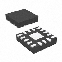
RHC PACKAGE
(TOP VIEW)
GND
QREF
IREF
IVIN
QVIN
P1dB of 7 dBm
–156 dBm/Hz Noise Floor
–150 dBm/Hz Noise at POUT = 0 dBm
Typical Unadjusted Carrier Suppression
> 35 dBc at 1 GHz
Typical Unadjusted Sideband Suppression
> 40 dBc at 1 GHz
Differential or Single-Ended I, Q Inputs
Convenient Single-Ended LO Input
Silicon Germanium Technology
1 16 15 14 13
GND
GND
LO
•
•
•
•
•
•
•
12
4
10
11
GND
GND
VCC
5 6 7 8 9
APPLICATIONS
•
2
3
GND
VCC
PWD
RFOUT
GND
•
•
•
•
Cellular Base Transceiver Station Transmit
Channel
IF Sampling Applications
TDMA: GSM, IS-136, EDGE/UWC-136
CDMA: IS-95, UMTS, CDMA2000
Wireless Local Loop
Wireless LAN IEEE 802.11
LMDS, MMDS
Wideband Baseband Transceivers
DESCRIPTION
The TRF3701 is an ultralow-noise direct quadrature modulator that is capable of converting complex input
signals from baseband or IF directly up to RF. An internal analog combiner sums the real and imaginary
components of the RF outputs. This combined output can feed the RF preamp directly at frequencies of up to 1.5
GHz. The modulator is implemented as a double-balanced mixer. An internal local oscillator (LO) phase splitter
accommodates a single-ended LO input, eliminating the need for a costly external balun.
AVAILABLE OPTIONS
TA
–40°C to 85°C
4-mm × 4-mm 16-Pin RHC (QFN) Package
TRF3701IRHC
TRF3701IRHCR (Tape and Reel)
Please be aware that an important notice concerning availability, standard warranty, and use in critical applications of Texas
Instruments semiconductor products and disclaimers thereto appears at the end of this data sheet.
PRODUCTION DATA information is current as of publication date.
Products conform to specifications per the terms of the Texas
Instruments standard warranty. Production processing does not
necessarily include testing of all parameters.
Copyright © 2003–2004, Texas Instruments Incorporated
�TRF3701
www.ti.com
SLWS145B – FEBRUARY 2003 – REVISED JUNE 2004
FUNCTIONAL BLOCK DIAGRAM
VCC
IVIN
IREF
+45°
LO
–45°
Σ
RFOUT
50 Ω
QVIN
QREF
PWD
GND
TERMINAL FUNCTIONS
TERMINAL
NAME
NO.
I/O
DESCRIPTION
GND
1, 2, 3, 5, 9, 11, 12
IREF
15
I
In-phase (I) reference voltage/differential input
IVIN
14
I
In-phase (I) signal input
LO
4
I
Local oscillator input
PWD
7
I
Power down
QREF
16
I
Quadrature (Q) reference voltage/differential input
QVIN
13
I
Quadrature (Q) signal input
RFOUT
8
O
RF output
VCC
Ground
6, 10
Supply voltage
ABSOLUTE MAXIMUM RATINGS
over operating free-air temperature range (unless otherwise noted) (1) (2)
VCC
TA
Supply voltage range
–0.5 V to 6 V
LO input power level
10 dBm
Baseband input voltage level (single-ended)
3 Vp-p
Operating free-air temperature range
Lead temperature for 10 seconds
(1)
(2)
2
–40°C to 85°C
260°C
Stresses beyond those listed under "absolute maximum ratings" may cause permanent damage to the device. These are stress ratings
only, and functional operation of the device at these or any other conditions beyond those indicated under "recommended operating
conditions" is not implied. Exposure to absolute-maximum-rated conditions for extended periods may affect device reliability.
Measured with respect to ground
�TRF3701
www.ti.com
SLWS145B – FEBRUARY 2003 – REVISED JUNE 2004
RECOMMENDED OPERATING CONDITIONS
MIN
NOM
MAX
4.5
5
5.5
UNIT
Supplies and References
VCC
Analog supply voltage
VCM (IVIN, QVIN, IREF, QREF input common-mode dc voltage)
3.7
V
V
Local Oscillator Input (LO)
Input frequency
400
Power level (measured into 50 Ω)
–6
1500
MHz
6
dBm
0
Signal Inputs (IVIN, QVIN)
Input bandwidth
700
MHz
ELECTRICAL CHARACTERISTICS
Over recommended operating conditions, VCC = 5 V, VCM = 3.7 V, fLO = 942.5 MHz at 0 dBm, TA = 25°C (unless otherwise
noted)
PARAMETER
TEST CONDITIONS
MIN
TYP
MAX
UNIT
Power Supply
ICC
Total supply current
V(PWD) = 5 V
145
V(PWD) = 0 V
13
Power-down input impedance
mA
11
kΩ
Turnon time
120
ns
Turnoff time
20
ns
40 + j4.8
Ω
16
µA
Local Oscillator (LO) Input
Input impedance
Signal Inputs (IVIN, QVIN, IREF, QREF)
Input bias current
Input impedance
V(IVIN) = V(IREF) = V(QVIN) = V(QREF) = VCM = 3.7 V
Single-ended input
250
Differential input
125
kΩ
3
�TRF3701
www.ti.com
SLWS145B – FEBRUARY 2003 – REVISED JUNE 2004
RF OUTPUT PERFORMANCE
Over recommended operating conditions, VCC = 5 V, VCM = 3.7 V, fLO = 942.5 MHz at 0 dBm, TA = 25°C (unless otherwise
noted) (1)
PARAMETER
TEST CONDITIONS
MIN
TYP
–3.5
–1
MAX
UNIT
Single and Two-Tone Specifications
Output power
Second baseband harmonic (USB or LSB) (3)
I, Q (2) = 1 Vp-p, fBB = 928 kHz
Third baseband harmonic
(USB or LSB) (3)
IMD3
I, Q (2) = 1 Vp-p (two-tone signal, fBB1 = 928 kHz,
fBB2 = 992 kHz)
P1dB (output compression
point)
NSD
Noise spectral density
dBc
–61
–55
dBc
–55
–45
dBc
dBm
–156
6-MHz offset from carrier, Pout = –10 dBm, over temperature
–153
–151 (5)
6-MHz offset from carrier, Pout = –5 dBm, over temperature
–152
–150 (5)
6-MHz offset from carrier, Pout = 0 dBm, over temperature
–150
–148 (5)
26 + j3
30
I, Q (2) = 1 Vp-p, fBB = 928 kHz, optimized
I,
Q (2)
I, Q (2) = 1 Vp-p, fBB = 928 kHz, optimized
I,
Q (2)
= 1 Vp-p, fBB = 928 kHz, over temperature
dBm/Hz
Ω
35
55
= 1 Vp-p, fBB = 928 kHz, over temperature
I, Q (2) = 1 Vp-p, fBB = 928 kHz, unadjusted
(1)
(2)
(3)
(4)
(5)
–45
I, Q (4) = VCM = 3.7 VDC
I, Q (2) = 1 Vp-p, fBB = 928 kHz, unadjusted
Sideband suppression
–50
6.5
RFOUT pin impedance
Carrier suppression
dBm
dBc
35
37
50
55
dBc
38
Baseband inputs are differential; equivalent performance is attained by using single-ended drive.
I , Q = 1 Vp-p implies that the magnitude of the signal at each input pin IVIN, IREF, QVIN, QREF is equal to 500 mVp-p.
USB = upper sideband. LSB = lower sideband.
All input pins tied to VCM
Maximum noise values are assured by statistical characterization only, not production testing. The values specified are over the entire
temperature range, TA = –40°C to 85°C.
DEFINITIONS OF SELECTED SPECIFICATIONS
Unadjusted Carrier Suppression
This specification measures the amount by which the local oscillator component is attenuated in the output
spectrum of the modulator relative to the carrier. It is assumed that the baseband inputs delivered to the pins of
the TRF3701 are perfectly matched to have the same dc offset (VCM). This includes all four baseband inputs:
IVIN, QVIN, IREF and QREF. Unadjusted carrier suppression is measured in dBc.
Adjusted (Optimized) Carrier Suppression
This differs from the unadjusted suppression number in that the dc offsets of the baseband inputs are iteratively
adjusted around their theoretical value of VCM in order to yield the maximum suppression of the LO component
in the output spectrum. Adjusted carrier suppression is measured in dBc.
Unadjusted Sideband Suppression
This specification measures the amount by which the unwanted sideband of the input signal is attenuated in the
output of the modulator, relative to the wanted sideband. It is assumed that the baseband inputs delivered to the
modulator input pins are perfectly matched in amplitude and are exactly 90° out of phase. Unadjusted sideband
suppression is measured in dBc.
4
�TRF3701
www.ti.com
SLWS145B – FEBRUARY 2003 – REVISED JUNE 2004
DEFINITIONS OF SELECTED SPECIFICATIONS (continued)
Adjusted (Optimized) Sideband Suppression
This differs from the unadjusted sideband suppression in that the baseband inputs are iteratively adjusted around
their theoretical values to maximize the amount of sideband suppression. Adjusted sideband suppression is
measured in dBc.
Suppressions Over Temperature
This specification assumes that the user has gone through the optimization process for the suppression in
question, and set the optimal settings for the I, Q inputs at room temperature. This specification then measures
the suppression when temperature conditions change after the initial calibration is done.
5
�TRF3701
www.ti.com
SLWS145B – FEBRUARY 2003 – REVISED JUNE 2004
TYPICAL CHARACTERISTICS
For all the performance plots in this section,
TA = –40°C to 85°C, VCC = 5 V, VCM = 3.7
differentially at a frequency of 50 kHz for an
suppressions, the point of optimization is noted
level of >50 dBc is assumed to be optimized.
the following conditions were used, unless otherwise noted:
V, fLO = 942.5 MHz at PLO = 0 dBm, I and Q inputs driven
output power level Pout = 0 dBm. In the case of optimized
and is always at nominal conditions and room temperature. A
OUTPUT POWER
vs
I, Q AMPLITUDE
OUTPUT POWER
vs
I, Q AMPLITUDE
10
10
5
–40°C
5
0
POUT − Output Power − dBm
POUT − Output Power − dBm
–40°C
85°C
25°C
−5
−10
−15
−20
85°C
0
25°C
−5
−10
−15
−20
fLO = 400 MHz
fLO = 942.5 MHz
−25
−25
0
1
2
3
4
I, Q Amplitude − VPP
0
1
2
3
4
I, Q Amplitude − VPP
G001
Figure 1.
Figure 2.
OUTPUT POWER
vs
I, Q AMPLITUDE
SECOND USB
vs
I, Q AMPLITUDE
G002
0
10
fLO = 400 MHz
−10
–40°C
0
−20
85°C
25°C
2nd USB − dBc
POUT − Output Power − dBm
5
−5
−10
−15
−30
−40
–40°C
−50
85°C
−60
−20
−70
fLO = 1500 MHz
25°C
−25
−80
0
1
2
I, Q Amplitude − VPP
Figure 3.
6
3
4
0
G003
1
2
I, Q Amplitude − VPP
Figure 4.
3
4
G004
�TRF3701
www.ti.com
SLWS145B – FEBRUARY 2003 – REVISED JUNE 2004
TYPICAL CHARACTERISTICS (continued)
SECOND USB
vs
I, Q AMPLITUDE
SECOND USB
vs
I, Q Amplitude
0
0
fLO = 942.5 MHz
fLO = 1500 MHz
−10
−10
−20
−30
2nd USB − dBc
2nd USB − dBc
−20
–40°C
−40
−50
−40
25°C
85°C
−60
25°C
85°C
−50
−70
−80
−60
0
1
2
3
4
0
I, Q Amplitude − VPP
2
3
4
G005
G006
Figure 5.
Figure 6.
UNADJUSTED CARRIER SUPPRESSION
vs
OUTPUT POWER
UNADJUSTED CARRIER SUPPRESSION
vs
OUTPUT POWER
80
CS − Unadjusted Carrier Suppression − dBc
fLO = 400 MHz
85°C
40
–40°C
25°C
30
20
10
0
−15
1
I, Q Amplitude − VPP
50
CS − Unadjusted Carrier Suppression − dBc
–40°C
−30
−10
−5
0
POUT − Output Power − dBm
Figure 7.
5
10
G007
fLO = 942.5 MHz
70
–40°C
60
50
40
25°C
85°C
30
20
10
0
−15
−10
−5
0
POUT − Output Power − dBm
5
10
G008
Figure 8.
7
�TRF3701
www.ti.com
SLWS145B – FEBRUARY 2003 – REVISED JUNE 2004
TYPICAL CHARACTERISTICS (continued)
UNADJUSTED CARRIER SUPPRESSION
vs
OUTPUT POWER
UNADJUSTED SIDEBAND SUPPRESSION
vs
OUTPUT POWER
60
SS − Unadjusted Sideband Suppression − dBc
CS − Unadjusted Carrier Suppression − dBc
80
fLO = 1500 MHz
70
60
50
40
–40°C
30
20
25°C
85°C
10
0
−15
−10
−5
0
5
25°C
85°C
20
10
G009
−20
−10
0
Figure 10.
UNADJUSTED SIDEBAND SUPPRESSION
vs
OUTPUT POWER
UNADJUSTED SIDEBAND SUPPRESSION
vs
OUTPUT POWER
10
G010
60
85°C
SS − Unadjusted Sideband Suppression − dBc
SS − Unadjusted Sideband Suppression − dBc
30
Figure 9.
50
40
25°C
–40°C
30
20
10
fLO = 942.5 MHz
−15
−5
POUT − Output Power − dBm
Figure 11.
8
–40°C
40
POUT − Output Power − dBm
60
0
−25
50
0
−30
10
POUT − Output Power − dBm
fLO = 400 MHz
fLO = 1500 MHz
50
–40°C
40
30
25°C
10
0
−30
5
G011
85°C
20
−20
−10
0
POUT − Output Power − dBm
Figure 12.
10
G012
�TRF3701
www.ti.com
SLWS145B – FEBRUARY 2003 – REVISED JUNE 2004
TYPICAL CHARACTERISTICS (continued)
THIRD LSB
vs
OUTPUT POWER
THIRD LSB
vs
OUTPUT POWER
0
0
fLO = 400 MHz
fLO = 942.5 MHz
−20
–40°C
−20
3rd LSB − dBc
3rd LSB − dBc
–40°C
−40
85°C
−60
−80
−40
85°C
−60
−80
25°C
−100
−30
25°C
−20
−10
0
−100
−30
10
POUT − Output Power − dBm
−20
−10
0
10
POUT − Output Power − dBm
G013
Figure 13.
Figure 14.
THIRD LSB
vs
OUTPUT POWER
IMD3
vs
OUTPUT POWER PER TONE
G014
0
0
fLO = 1500 MHz
fLO = 400 MHz
−10
−20
−40
IMD3 − dBc
3rd LSB − dBc
−20
85°C
−60
–40°C
−30
−40
−50
85°C
–40°C
−60
−80
−70
25°C
−100
−30
−20
−10
0
POUT − Output Power − dBm
Figure 15.
10
G015
−80
−15
25°C
−10
−5
POUT − Output Power Per Tone − dBm
0
G016
Figure 16.
9
�TRF3701
www.ti.com
SLWS145B – FEBRUARY 2003 – REVISED JUNE 2004
TYPICAL CHARACTERISTICS (continued)
IMD3
vs
OUTPUT POWER PER TONE
IMD3
vs
OUTPUT POWER PER TONE
0
0
fLO = 942.5 MHz
fLO = 1500 MHz
−10
−10
−20
IMD3 − dBc
IMD3 − dBc
−20
−30
25°C
−40
85°C
−30
−40
85°C
−50
–40°C
−50
−60
–40°C
−60
−70
25°C
−70
−15
−10
−5
−80
−15
0
POUT − Output Power Per Tone − dBm
G017
P1dB
vs
FREQUENCY
UNADJUSTED CARRIER SUPPRESSION
vs
FREQUENCY
G018
60
CS − Unadjusted Carrier Suppression − dBc
7
6
P1dB − dBm
0
Figure 18.
25°C
85°C
–40°C
4
3
2
1
0
85°C
50
40
25°C
30
20
–40°C
10
0
0
500
1000
1500
fLO − Frequency − MHz
Figure 19.
10
−5
Figure 17.
8
5
−10
POUT − Output Power Per Tone − dBm
2000
G019
0
500
1000
1500
fLO − Frequency − MHz
Figure 20.
2000
G020
�TRF3701
www.ti.com
SLWS145B – FEBRUARY 2003 – REVISED JUNE 2004
TYPICAL CHARACTERISTICS (continued)
UNADJUSTED SIDEBAND SUPPRESSION
vs
FREQUENCY
OUTPUT POWER FLATNESS
vs
FREQUENCY (POUT = 0, –10 dBm NOMINAL)
2
25°C
85°C
POUT − Output Power Flatness − dBm
SS − Unadjusted Sideband Suppression − dBc
60
50
40
25°C
30
–40°C
20
10
0
−2
–40°C
85°C
−4
−6
−8
25°C
85°C
−10
–40°C
−12
850
0
0
500
1000
1500
fLO − Frequency − MHz
2000
900
950
1000
fLO − Frequency − MHz
G021
Figure 21.
Figure 22.
SECOND USB
vs
FREQUENCY
THIRD LSB
vs
FREQUENCY
1050
G022
−40
−40
POUT = 0 dBm
POUT = 0 dBm
−45
−45
−50
3rd LSB − dBc
2nd USB − dBc
85°C
–40°C
−50
−55
−60
−65
25°C
25°C
−55
–40°C
−70
85°C
−75
−60
850
900
950
1000
fLO − Frequency − MHz
Figure 23.
1050
G023
−80
850
900
950
1000
fLO − Frequency − MHz
1050
G024
Figure 24.
11
�TRF3701
www.ti.com
SLWS145B – FEBRUARY 2003 – REVISED JUNE 2004
TYPICAL CHARACTERISTICS (continued)
CARRIER SUPPRESSION
vs
FREQUENCY
SIDEBAND SUPPRESSION
vs
FREQUENCY
80
85°C
25°C
SS − Sideband Suppression − dBc
CS − Carrier Suppression − dBc
80
60
–40°C
40
Optimization
Point
20
85°C
900
Optimization
Point
20
POUT = 0 dBm
Optimized at 942.5 MHz
950
1000
fLO − Frequency − MHz
0
850
1050
900
950
1000
fLO − Frequency − MHz
G025
Figure 25.
Figure 26.
OUTPUT POWER FLATNESS
vs
VCM (POUT = 0 dBm NOMINAL)
CARRIER SUPPRESSION
vs
VCM
4
G026
85°C
CS − Carrier Suppression − dBc
60
2
–40°C
25°C
0
85°C
−2
50
3.5
4.0
4.5
5.0
VCM − V
25°C
–40°C
40
Optimization
Point
30
20
10
−4
3.0
0
3.0
POUT = 0 dBm
fLO = 942.5 MHz
Optimized at 3.7 V
3.5
4.0
4.5
VCM − V
G027
Figure 27.
12
1050
70
fLO = 942.5 MHz
POUT − Output Power Flatness− dBm
–40°C
40
POUT = 0 dBm
Optimized at 942.5 MHz
0
850
25°C
60
G028
Figure 28.
�TRF3701
www.ti.com
SLWS145B – FEBRUARY 2003 – REVISED JUNE 2004
TYPICAL CHARACTERISTICS (continued)
SIDEBAND SUPPRESSION
vs
VCM
SECOND USB
vs
VCM
60
−30
25°C
−40
–40°C
–40°C
25°C
50
−50
85°C
2nd USB − dBc
SS − Sideband Suppression − dBc
70
40
Optimization
Point
30
−60
85°C
−70
20
10
−80
POUT = 0 dBm
fLO = 942.5 MHz
Optimized at 3.7 V
0
3.0
POUT = 0 dBm
fLO = 942.5 MHz
3.5
4.0
−90
3.0
4.5
3.5
VCM − V
G029
4.5
G030
Figure 29.
Figure 30.
THIRD LSB
vs
VCM
SUPPLY CURRENT
vs
SUPPLY VOLTAGE
0
−10
4.0
VCM − V
200
POUT = 0 dBm
fLO = 942.5 MHz
fLO = 942.5 MHz
ICC − Supply Current − mA
180
3rd LSB − dBc
−20
−30
–40°C
−40
85°C
−50
85°C
160
25°C
140
–40°C
120
−60
25°C
−70
3.0
3.5
4.0
4.5
VCM − V
G031
Figure 31.
100
4.0
4.5
5.0
5.5
VCC − Supply Voltage − V
6.0
G032
Figure 32.
13
�TRF3701
www.ti.com
SLWS145B – FEBRUARY 2003 – REVISED JUNE 2004
TYPICAL CHARACTERISTICS (continued)
OUTPUT POWER FLATNESS
vs
SUPPLY VOLTAGE (POUT = 0 dBm NOMINAL)
CARRIER SUPPRESSION
vs
SUPPLY VOLTAGE
80
3
fLO = 942.5 MHz
70
1
CS − Carrier Suppression − dBc
POUT − Output Power − dBm
2
25°C
–40°C
0
85°C
−1
−2
−3
4.0
60
50
25°C
5.0
5.5
VCC − Supply Voltage − V
20
4.5
5.0
5.5
G033
Figure 33.
Figure 34.
SIDEBAND SUPPRESSION
vs
SUPPLY VOLTAGE
SECOND USB
vs
SUPPLY VOLTAGE
6.0
G034
0
POUT = 0 dBm
fLO = 942.5 MHz
70
25°C
−10
85°C
60
−20
50
–40°C
40
30
2nd USB − dBc
SS − Sideband Suppression − dBc
POUT = 0 dBm
fLO = 942.5 MHz
Optimized at 5 V
VCC − Supply Voltage − V
80
Optimization
Point
−30
−40
25°C
20
10
0
4.0
−50
POUT = 0 dBm
fLO = 942.5 MHz
Optimized at 5 V
4.5
5.0
5.5
VCC − Supply Voltage − V
Figure 35.
14
Optimization
Point
30
0
4.0
6.0
–40°C
40
10
4.5
85°C
6.0
G035
−60
4.0
85°C
4.5
–40°C
5.0
5.5
VCC − Supply Voltage − V
Figure 36.
6.0
G036
�TRF3701
www.ti.com
SLWS145B – FEBRUARY 2003 – REVISED JUNE 2004
TYPICAL CHARACTERISTICS (continued)
THIRD LSB
vs
SUPPLY VOLTAGE
OUTPUT POWER FLATNESS
vs
LO INPUT POWER (POUT = 0 dBm NOMINAL)
0
fLO = 942.5 MHz
POUT − Output Power Flatness − dBm
−10
3
POUT = 0 dBm
fLO = 942.5 MHz
−30
−40
85°C
−50
−60
−70
–40°C
1
25°C
–40°C
0
85°C
−1
−2
25°C
−80
4.0
4.5
5.0
5.5
−3
−15
6.0
VCC − Supply Voltage − V
−10
−5
0
5
10
PLO − Local Oscillator Input Power − dBm
G037
Figure 37.
15
G038
Figure 38.
CARRIER SUPPRESSION
vs
LOCAL OSCILLATOR INPUT POWER
80
70
CS − Carrier Suppression − dBc
3rd LSB − dBc
−20
2
85°C
25°C
60
50
–40°C
40
Optimization
Point
30
20
10
0
−15
POUT = 0 dBm
fLO = 942.5 MHz
Optimized at 0 dBm
−10
−5
0
5
10
PLO − Local Oscillator Input Power − dBm
15
G039
Figure 39.
15
�TRF3701
www.ti.com
SLWS145B – FEBRUARY 2003 – REVISED JUNE 2004
Table 1. RFOUT and LO Pin Impedance
Frequency (MHz)
Z (RFOUT Pin)
Z (LO Pin)
100
8.59 – j 130.2
33.95 – j 106.93
200
7.12 – j 61.22
29.54 – j 52.57
300
8.52 – j 36.37
28.65 - j 31.83
400
10.5 – j 23.72
29.371 – j 19.33
500
12.82 – j 15.51
30.78 – j 11.42
600
15.26 – j 9.33
32.64 – j 6.06
700
187.1 – j 4.77
34.99 – j 1.65
800
20.8 – j 1.2
36.55 + j 1.65
900
24.2 + j 2.0
38.52 + j 3.98
1000
28.7 + j 4.9
40.29 + j 5.92
1100
32.35 + j 6.61
42.21 + j 6.98
1200
37.15 + j 6.88
44.09 + j 7.55
1300
40.55 + j 6.64
45.7 + j 7.96
1400
43.76 + j 6.4
47 + j 7.76
1500
46.6 + j 6.03
48.28 + j 7.39
SIDEBAND SUPPRESSION
vs
LOCAL OSCILLATOR INPUT POWER
SECOND USB
vs
LOCAL OSCILLATOR INPUT POWER
−35
POUT = 0 dBm
fLO = 942.5 MHz
60
50
−45
25°C
40
Optimization
Point
30
–40°C
−50
25°C
−55
20
–40°C
10
0
−15
−60
POUT = 0 dBm
fLO = 942.5 MHz
Optimized at 0 dBm
−10
−5
0
5
10
PLO − Local Oscillator Input Power − dBm
Figure 40.
16
−40
85°C
2nd USB − dBc
SS − Sideband Suppression − dBc
70
15
G040
−65
−15
85°C
−10
−5
0
5
10
PLO − Local Oscillator Input Power − dBm
Figure 41.
15
G041
�TRF3701
www.ti.com
SLWS145B – FEBRUARY 2003 – REVISED JUNE 2004
THIRD LSB
vs
LOCAL OSCILLATOR INPUT POWER
NOISE DISTRIBUTION AT 6 MHZ
OFFSET OVER TEMPERATURE
20
−40
POUT = 0 dBm
fLO = 942.5 MHz
18
85°C
−50
16
25°C
14
−70
Percentage
−60
3rd LSB − dBc
POUT = 0 dBm
fLO = 942.5 MHz
–40°C
−80
12
10
8
6
4
−90
−148.4
−148.6
−148.8
G042
−149.0
PLO − Local Oscillator Input Power − dBm
−149.2
15
−149.4
10
−149.6
5
−149.8
0
−150.0
−5
−150.2
0
−10
−150.4
−100
−15
−150.6
2
Noise − dBm/Hz
G043
Figure 42.
Figure 43.
NOISE DISTRIBUTION AT 6 MHZ
OFFSET OVER TEMPERATURE
NOISE DISTRIBUTION AT 6 MHZ
OFFSET OVER TEMPERATURE
18
16
14
14
12
12
Noise − dBm/Hz
−152.2
−152.4
−152.6
−152.8
Noise − dBm/Hz
G044
Figure 44.
−153.0
−153.2
−153.4
−153.6
−151.0
−151.2
−151.4
−151.6
0
−151.8
0
−152.0
2
−152.2
2
−152.4
4
−152.6
4
−152.8
6
−153.0
6
−153.8
8
−154.0
8
10
−154.2
10
POUT = –10 dBm
fLO = 942.5 MHz
−154.4
Percentage
16
−153.2
Percentage
18
20
POUT = –5 dBm
fLO = 942.5 MHz
−154.6
20
G045
Figure 45.
17
�TRF3701
www.ti.com
SLWS145B – FEBRUARY 2003 – REVISED JUNE 2004
NOISE AT 6 MHz OFFSET
vs
OUTPUT POWER
GMSK SPECTRAL PERFORMANCE
vs
CHANNEL POWER
−135
0
GMSK Spectral Performance − dBc in 30 kHz
fLO = 942.5 MHz
Noise − dBm/Hz
−140
−145
25°C
85°C
−150
−155
−160
−15
–40°C
−10
−5
0
5
−20
−30
−40
−50
−60
400 kHz Offset
−70
−80
600 kHz Offset
−90
−100
−12
10
POUT − Output Power − dBm
fLO = 942.5 MHz
−10
−10
−8
−6
Figure 47.
2.5
fLO = 942.5 MHz
2.0
1.5
1.0
0.5
0.0
−12 −10
0
2
4
G047
GSM EDGE EVM
vs
CHANNEL POWER
GSM Edge EVM − %
−2
G046
Figure 46.
−8
−6
−4
−2
0
2
4
6
Channel Power − dBm
G048
Figure 48.
18
−4
Channel Power − dBm
�TRF3701
www.ti.com
SLWS145B – FEBRUARY 2003 – REVISED JUNE 2004
THEORY OF OPERATION
The TRF3701 employs a double-balanced mixer architecture in implementing the direct I, Q upconversion. The I,
Q inputs can be driven single-endedly or differentially, with comparable performance in both cases. The common
mode level (VCM) of the four inputs (IVIN, IREF, QVIN, QREF) is typically set to 3.7 V and needs to be driven
externally. These inputs go through a set of differential amplifiers and through a V-I converter feed the
double-balanced mixers. The AC-coupled LO input to the device goes through a phase splitter to provide the
in-phase and quadrature signals that in turn drive the mixers. The outputs of the mixers are then summed,
converted to single-ended signals, and amplified before they are fed to the output port RFOUT. The output of the
TRF3701 is ac-coupled and can drive 50-Ω loads.
EQUIVALENT CIRCUITS
Figure 49 through Figure 52 show equivalent schematics for the main inputs and outputs of the device.
LO
50 Ω
IQ Baseband
S0001-01
S0002-01
Figure 49. LO Equivalent Input Circuit
Figure 50. IVIN, QVIN, IREF, QREF Equivalent Circuit
50 kΩ
Power Down
RFOUT
S0004-01
S0003-01
Figure 51. RFOUT Equivalent Circuit
Figure 52. Power-Down (PWD) Equivalent Circuit
19
�TRF3701
www.ti.com
SLWS145B – FEBRUARY 2003 – REVISED JUNE 2004
APPLICATION INFORMATION
DRIVING THE I, Q INPUTS
There are several ways to drive the four baseband inputs of the TRF3701 to the required amplitude and dc
offset. The optimal configuration depends on the end application requirements and the signal levels desired by
the designer.
The TRF3701 is by design a differential part, meaning that ideally the user should provide fully complementary
signals. However, similar performance in every respect can be achieved if the user only has single-ended signals
available. In this case, the IREF and QREF pins just need to have the VCM dc offset applied.
Implementing a Single-to-Differential Conversion for the I, Q inputs
In case differential I, Q signals are desired but not available, the THS4503 family of wideband, low-distortion, fully
differential amplifiers can be used to provide a convenient way of performing this conversion. Even if differential
signals are available, the THS4503 can provide gain in case a higher voltage swing is required. Besides featuring
high bandwidth and high linearity, the THS4503 also provides a convenient way of applying the VCM to all four
inputs to the modulator through the VOCM pin (pin 2). The user can further adjust the dc levels for optimum
carrier suppression by injecting extra dc at the inputs to the operational amplifier, or by individually adding it to
the four outputs. Figure 53 shows a typical implementation of the THS4503 as a driver for the TRF3701. Gain
can be easily incorporated in the loop by adjusting the feedback resistors appropriately. For more details, see the
THS4503 data sheet at www.ti.com.
20
�TRF3701
www.ti.com
SLWS145B – FEBRUARY 2003 – REVISED JUNE 2004
APPLICATION INFORMATION (continued)
10 pF
392 Ω
+8 VA
VCM
0.01 µF
0.1 µF
0.01 µF
7
3
+VCC
NC
374 Ω
Single-Ended I Input
8
2
402 Ω
0.1 µF
THS4503
5
22.1 Ω
4
22.1 Ω
IREF
VOUT−
VOCM
VOUT+
1
IREF
+
−
IVIN
IVIN
−VCC
6
−8 VA
0.1 µF
0.01 µF
392 Ω
10 pF
S0005-02
Figure 53. Using the THS4503 to Condition the Baseband Inputs to the TRF3701 (I Channel Shown)
DRIVING THE LOCAL OSCILLATOR INPUT
The LO pin is internally terminated to 50 Ω, thus enabling easy interface to the LO source without the need for
external impedance matching. The power level of the LO signal should be in the range of –6 to 6 dBm. For
characterization purposes, a power level of 0 dBm was chosen. An ideal way of driving the LO input of the
TRF3701 is by using the TRF3750, an ultralow-phase-noise integer-N PLL from Texas Instruments. Combining
the TRF3750 with an external VCO can complete the loop and provide a flexible, convenient and cost-effective
21
�TRF3701
www.ti.com
SLWS145B – FEBRUARY 2003 – REVISED JUNE 2004
APPLICATION INFORMATION (continued)
solution for the local oscillator of the transmitter. Figure 54 shows a typical application for the LO driver network
that incorporates the TRF3750 integer-N PLL synthesizer into the design. Depending on the VCO output and the
amount of signal loss, an optional gain stage may be added to the output of the VCO before it is applied to the
TRF3701 LO input.
DVDD
10 pF
+
VCP
AVDD
VVCO
0.1 �F
0.1 �F
+
10 pF
10 pF
10 �F
10 pF
CE
VCP
16
16.5 �
1 nF
TCXO
(10-MHz
Reference)
8
100 pF
15
7
10
+
10 �F
0.1 �F
AVDD
SUPPLY
GND
To TRF3701
LO Input
+
0.1 �F
10 �F
DVDD
10 �F
REFIN
CPOUT
20 k�
2
1 nF
TRF3750
10 nF
V TUNE
82 pF
GND
RSET
1
RFINA
6
DECOUPLING NOT SHOWN
OUT
VCO
16.5 �
100 pF
GND
16.5 �
3.9 k�
RSET
4.7 k�
12
LE
13
DATA
LE
MUXOUT
14 LOCK DETECT
DGND
DATA
CLK
CPGND
11
AGND
CLK
5
3 4 9
RFINB
100 pF
49.9 �
100 pF
Figure 54. Typical Application Circuit for Generating the LO Signal for the TRF3701 Modulator
PCB LAYOUT CONSIDERATIONS
The TRF3701 is a high-performance RF device; hence, care should be taken in the layout of the PCB in order to
ensure optimum performance. Proper decoupling with low ESR capacitors is needed for the VCC supplies (pins
6 and 10). Typical values used are in the order of 1 pF in parallel to 0.1 µF, with the lower-valued capacitors
placed closer to the device pins. In addition, a larger tank capacitor in the order of 10 µF should be placed on the
supply line as layout permits. At least a 4-layer board is recommended for the PCB. If possible, a solid ground
plane and a ground pour is also recommended, as is a power plane for the supplies. Because the balance of the
four I, Q inputs to the modulator can be critical to device performance, care should be taken to ensure that the
trace runs for all four inputs are equidistant. In the case of single-ended drive of the I, Q inputs, the two unused
pins IREF and QREF are fed with the VCM dc voltage only, and should be decoupled with a 0.1-µF capacitor (or
smaller). The LO input trace should be minimized in length and have controlled impedance of 50 Ω. No external
matching components are needed because there is an internal 50-Ω termination. The RFOUT pin should also
have a relatively small trace to minimize parasitics and coupling, and should also be controlled to 50 Ω. An
impedance-matching network can be used to optimize power transfer, but is not critical. All the results shown in
the data sheet were taken with no impedance matching network used (RFOUT directly driving an external 50-Ω
load).
The exposed thermal and ground pad on the bottom of the TRF3701 should be soldered to ground to ensure
optimum electrical and thermal performance. The landing pattern on the PCB should include a solid pad and 4
thermal vias. These vias typically have 1,2-mm pitch and 0,3-mm diameter. The vias can be arranged in a 2×2
array. The thermal pad on the PCB should be at least 1.65×1.65 mm.
IMPLEMENTING A DIRECT UPCONVERSION TRANSMITTER USING A TI CommsDAC
The TRF3701 is ideal for implementing a direct upconversion transmitter, where the input I, Q data can originate
from an ASIC or a DAC. Texas Instruments' line of digital-to-analog converters (DAC) is ideally suited for
interfacing to the TRF3701. Such DACs include, among others, the DAC290x series, DAC5672, and DAC5686.
22
�TRF3701
www.ti.com
SLWS145B – FEBRUARY 2003 – REVISED JUNE 2004
APPLICATION INFORMATION (continued)
This section illustrates the use of the DAC5686, which offers a unique set of features that make interfacing to the
TRF3701 easy and convenient. The DAC5686 is a 16-bit, 500 MSPS, 2×–16× interpolating dual-channel DAC,
and it features I, Q adjustments for optimal interface to the TRF3701. User-selectable, 11-bit offset and 12-bit
gain adjustments can optimize the carrier and sideband suppression of the modulator, resulting in enhanced
performance and relaxed filtering requirements at RF. The preferred mode of operation of the DAC5686 for direct
interface with the TRF3701 at baseband is the dual-DAC mode. The user also has the flexibility of selecting any
one of the four possible complex spectral bands to be fed into the TRF3701. For details on the available modes
and programming, see the DAC5686 data sheet available at www.ti.com.
Figure 55 shows the DAC5686 in dual-DAC mode, which is best-suited for zero-IF interface to the TRF3701. In
this mode, a seamless, passive interface between the DAC output and the input to the modulator is used, so that
no extra components are needed between the two devices. The optimum dc offset level for the inputs to the
TRF3701 (VCM) is approximately 3.7 V. The output of the DAC should be centered around 3.3 V or less
(depending on signal swing), in order to ensure that its output compliance limits are not exceeded. The resistive
network shown in Figure 55 allows for this dc offset transition while still providing a dc path between the DAC
output and the modulator. This ensures that the dc offset adjustments on the DAC5686 can still be applied to
optimize the carrier suppression at the modulator output. The combination of the DAC5686 and the TRF3701
provides a unique signal-chain solution with state-of-the-art performance for wireless infrastructure applications.
+3.3 V
+5 V
VCC
Fdata
A
Offset
IOUTA1
IVIN
IREF
DEMUX
16-Bit
DAC
IOUTA2
DA[15:0]
A Gain
+45°
LO
B Gain
B
Offset
Σ
RFOUT
50 Ω
16-Bit
DAC
DB[15:0]
–45°
IOUTB1
QVIN
IOUTB2
QREF
DAC5686
TRF3701
PWD
+3.3 V
GND
+5 V
Figure 55. DAC5686 in Dual-DAC Mode with Quadrature Modulator
23
�MECHANICAL DATA
MPQF132 – JUNE 2002
RHC (S–PQFP–N16)
(CUSTOM PACKAGE)
4,15
PLASTIC QUAD FLATPACK
A
3,85
B
ÏÏÏÏ
ÏÏÏÏ
ÏÏÏÏ
ÏÏÏÏ
4,15
3,85
16
1
PIN 1 INDEX AREA
TOP AND BOTTOM
2
1,00
0,80
0,20 NOMINAL
LEAD FRAME
0,08 C
SEATING PLANE
0,05
0,00
C
1,65 MAX
16�
0,80
PIN 1 CHAMBER
0,725
0,525
2
5
1
16
1,65 MAX
9
EXPOSED THERMAL DIE PAD
12
D
16�
0,435
0,315
BOTTOM VIEW
0,10
4204353/A 05/02
NOTES: A. All linear dimensions are in millimeters.
B. This drawing is subject to change without notice.
C. QFN (Quad Flatpack No–Lead) Package configuration.
D. The Package thermal performance may be enhanced by bonding the thermal die pad to an external thermal plane. This pad is
electrically and thermally connected to the backside of the die and possibly selected ground leads.
POST OFFICE BOX 655303
• DALLAS, TEXAS 75265
1
��IMPORTANT NOTICE
Texas Instruments Incorporated and its subsidiaries (TI) reserve the right to make corrections, modifications,
enhancements, improvements, and other changes to its products and services at any time and to discontinue
any product or service without notice. Customers should obtain the latest relevant information before placing
orders and should verify that such information is current and complete. All products are sold subject to TI’s terms
and conditions of sale supplied at the time of order acknowledgment.
TI warrants performance of its hardware products to the specifications applicable at the time of sale in
accordance with TI’s standard warranty. Testing and other quality control techniques are used to the extent TI
deems necessary to support this warranty. Except where mandated by government requirements, testing of all
parameters of each product is not necessarily performed.
TI assumes no liability for applications assistance or customer product design. Customers are responsible for
their products and applications using TI components. To minimize the risks associated with customer products
and applications, customers should provide adequate design and operating safeguards.
TI does not warrant or represent that any license, either express or implied, is granted under any TI patent right,
copyright, mask work right, or other TI intellectual property right relating to any combination, machine, or process
in which TI products or services are used. Information published by TI regarding third-party products or services
does not constitute a license from TI to use such products or services or a warranty or endorsement thereof.
Use of such information may require a license from a third party under the patents or other intellectual property
of the third party, or a license from TI under the patents or other intellectual property of TI.
Reproduction of information in TI data books or data sheets is permissible only if reproduction is without
alteration and is accompanied by all associated warranties, conditions, limitations, and notices. Reproduction
of this information with alteration is an unfair and deceptive business practice. TI is not responsible or liable for
such altered documentation.
Resale of TI products or services with statements different from or beyond the parameters stated by TI for that
product or service voids all express and any implied warranties for the associated TI product or service and
is an unfair and deceptive business practice. TI is not responsible or liable for any such statements.
Following are URLs where you can obtain information on other Texas Instruments products and application
solutions:
Products
Applications
Amplifiers
amplifier.ti.com
Audio
www.ti.com/audio
Data Converters
dataconverter.ti.com
Automotive
www.ti.com/automotive
DSP
dsp.ti.com
Broadband
www.ti.com/broadband
Interface
interface.ti.com
Digital Control
www.ti.com/digitalcontrol
Logic
logic.ti.com
Military
www.ti.com/military
Power Mgmt
power.ti.com
Optical Networking
www.ti.com/opticalnetwork
Microcontrollers
microcontroller.ti.com
Security
www.ti.com/security
Telephony
www.ti.com/telephony
Video & Imaging
www.ti.com/video
Wireless
www.ti.com/wireless
Mailing Address:
Texas Instruments
Post Office Box 655303 Dallas, Texas 75265
Copyright 2004, Texas Instruments Incorporated
�