Product
Folder
Sample &
Buy
Support &
Community
Tools &
Software
Technical
Documents
TRF370417
SLWS213A – JANUARY 2010 – REVISED NOVEMBER 2015
TRF370417 50-MHz to 6-GHz Quadrature Modulator
1 Features
3 Description
•
The TRF370417 is a low-noise direct quadrature
modulator, capable of converting complex modulated
signals from baseband or IF directly up to RF. The
TRF370417 is a high-performance, superior-linearity
device that operates at RF frequencies of 50 MHz
through 6 GHz. The modulator is implemented as a
double-balanced mixer. The RF output block consists
of a differential to single-ended converter and an RF
amplifier capable of driving a single-ended 50-Ω load
without any need of external components. The
TRF370417 requires a 1.7-V common-mode voltage
for optimum linearity performance.
TRF370417
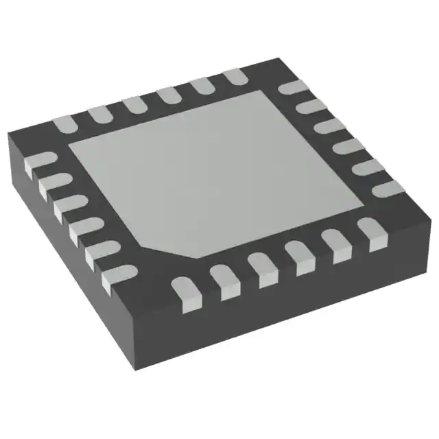
BODY SIZE (NOM)
VQFN(24)
4.00 mm × 4.00 mm
(1) For all available packages, see the orderable addendum at
the end of the data sheet.
BBIN
BBIP
GND
GND
21
20
19
Block Diagram
22
Cellular Base Station Transceiver
CDMA: IS95, UMTS, CDMA2000, TD-SCDMA
TDMA: GSM, IS-136, EDGE/UWC-136
Multicarrier GSM
WiMAX: 802.16d/e
3GPP: LTE
Point-to-Point (P2P) Microwave
Wideband Software-Defined Radio
Public Safety: TETRA/APC025
Communication-System Testers
Cable Modem Termination System (CMTS)
PACKAGE
GND
•
•
•
•
•
•
•
•
•
•
•
PART NUMBER
23
2 Applications
Device Information(1)
VCC
•
•
•
•
•
•
•
•
76-dBc Single-Carrier WCDMA ACPR at –8 dBm
Channel Power
Low Noise Floor: –162.3 dBm/Hz at 2140 MHz
OIP3 of 26.5 dBm at 2140 MHz
P1dB of 12 dBm at 2140 MHz
Carrier Feedthrough of –38 dBm at 2140 MHz
Side-Band Suppression of –50 dBc at 2140 MHz
Single Supply: 4.5-V–5.5-V Operation
Silicon Germanium Technology
1.7-V CM at I, Q Baseband Inputs
24
1
NC
1
18
VCC
GND
2
17
GND
LOP
3
16
RF_OUT
S
0/90
12
NC
GND
13
11
6
GND
NC
10
GND
BBQP
14
9
5
BBQN
GND
8
NC
GND
15
7
4
NC
LON
B0175-01
1
An IMPORTANT NOTICE at the end of this data sheet addresses availability, warranty, changes, use in safety-critical applications,
intellectual property matters and other important disclaimers. PRODUCTION DATA.
�TRF370417
SLWS213A – JANUARY 2010 – REVISED NOVEMBER 2015
www.ti.com
Table of Contents
1
2
3
4
5
6
7
Features ..................................................................
Applications ...........................................................
Description .............................................................
Revision History.....................................................
Pin Configuration and Functions .........................
Specifications.........................................................
1
1
1
2
3
4
6.1
6.2
6.3
6.4
6.5
6.6
6.7
4
4
4
4
5
5
8
Absolute Maximum Ratings ......................................
ESD Ratings..............................................................
Recommended Operating Conditions.......................
Thermal Information ..................................................
Electrical Characteristics...........................................
RF Output Parameters ..............................................
Typical Characteristics ..............................................
Detailed Description ............................................ 16
7.1 Overview ................................................................. 16
7.2 Functional Block Diagram ....................................... 16
7.3 Feature Description................................................. 16
7.4 Device Functional Modes........................................ 16
8
Application and Implementation ........................ 18
8.1 Application Information............................................ 18
8.2 Typical Application ................................................. 20
9 Power Supply Recommendations...................... 23
10 Layout................................................................... 23
10.1 Layout Guidelines ................................................. 23
10.2 Layout Example .................................................... 23
11 Device and Documentation Support ................. 25
11.1
11.2
11.3
11.4
11.5
11.6
Device Support......................................................
Documentation Support ........................................
Community Resources..........................................
Trademarks ...........................................................
Electrostatic Discharge Caution ............................
Glossary ................................................................
25
26
26
26
26
26
12 Mechanical, Packaging, and Orderable
Information ........................................................... 26
4 Revision History
NOTE: Page numbers for previous revisions may differ from page numbers in the current version.
Changes from Original (January 2010) to Revision A
•
2
Page
Added ESD Ratings table, Feature Description section, Device Functional Modes, Application and Implementation
section, Power Supply Recommendations section, Layout section, Device and Documentation Support section, and
Mechanical, Packaging, and Orderable Information section. ................................................................................................. 1
Submit Documentation Feedback
Copyright © 2010–2015, Texas Instruments Incorporated
Product Folder Links: TRF370417
�TRF370417
www.ti.com
SLWS213A – JANUARY 2010 – REVISED NOVEMBER 2015
5 Pin Configuration and Functions
VCC
GND
BBIN
BBIP
GND
GND
24
23
22
21
20
19
RGE Package
24-Pin VQFN With Exposed Thermal Pad
Top View
LON
4
15
NC
GND
5
14
GND
NC
6
13
NC
12
RF_OUT
GND
16
11
3
GND
LOP
10
GND
BBQP
17
9
2
BBQN
GND
8
VCC
GND
18
7
1
NC
NC
Pin Functions
PIN
NAME
NO.
I/O
DESCRIPTION
BBIN
22
I
In-phase negative input
BBIP
21
I
In-phase positive input
BBQN
9
I
Quadrature-phase negative input
BBQP
10
I
Quadrature-phase positive input
GND
2, 5, 8, 11,
12, 14, 17,
19, 20, 23
—
LON
4
I
Local oscillator (LO) negative input
LOP
3
I
Local oscillator (LO) positive input
NC
1, 6, 7, 13,
15
—
No connect
16
O
RF output
18, 24
—
Power supply
RF_OUT
VCC
Ground
Submit Documentation Feedback
Copyright © 2010–2015, Texas Instruments Incorporated
Product Folder Links: TRF370417
3
�TRF370417
SLWS213A – JANUARY 2010 – REVISED NOVEMBER 2015
www.ti.com
6 Specifications
6.1 Absolute Maximum Ratings
over operating free-air temperature range (unless otherwise noted) (1)
MIN
MAX
UNIT
Supply voltage range
–0.3
6
V
TJ
Operating virtual junction temperature range
–40
150
°C
TA
Operating ambient temperature range
–40
85
°C
Tstg
Storage temperature range
–65
150
°C
(1)
Stresses beyond those listed under Absolute Maximum Ratings may cause permanent damage to the device. These are stress ratings
only, which do not imply functional operation of the device at these or any other conditions beyond those indicated under Recommended
Operating Conditions. Exposure to absolute-maximum-rated conditions for extended periods may affect device reliability.
6.2 ESD Ratings
VALUE
V(ESD)
(1)
(2)
Electrostatic discharge
Human-body model (HBM), per ANSI/ESDA/JEDEC JS-001 (1)
±75
Charged-device model (CDM), per JEDEC specification JESD22C101 (2)
±75
UNIT
V
JEDEC document JEP155 states that 500-V HBM allows safe manufacturing with a standard ESD control process.
JEDEC document JEP157 states that 250-V CDM allows safe manufacturing with a standard ESD control process.
6.3 Recommended Operating Conditions
over operating free-air temperature range (unless otherwise noted)
VCC
Power-supply voltage
MIN
NOM
MAX
4.5
5
5.5
UNIT
V
6.4 Thermal Information
TRF370417
THERMAL METRIC
(1)
RGE (VQFN)
UNIT
24 PINS
RθJA
Junction-to-ambient thermal resistance (High-K board, still air)
29.4
°C/W
RθJC(top)
Junction-to-case (top) thermal resistance
18.6
°C/W
RθJB
Junction-to-board thermal resistance
14
°C/W
ψJT
Junction-to-top characterization parameter
—
°C/W
ψJB
Junction-to-board characterization parameter
—
°C/W
RθJC(bot)
Junction-to-case (bottom) thermal resistance
—
°C/W
(1)
4
For more information about traditional and new thermal metrics, see the Semiconductor and IC Package Thermal Metrics application
report, SPRA953.
Submit Documentation Feedback
Copyright © 2010–2015, Texas Instruments Incorporated
Product Folder Links: TRF370417
�TRF370417
www.ti.com
SLWS213A – JANUARY 2010 – REVISED NOVEMBER 2015
6.5 Electrical Characteristics
over operating free-air temperature range (unless otherwise noted)
PARAMETER
TEST CONDITIONS
MIN
TYP
MAX
UNIT
205
245
mA
6
GHz
12
dBm
DC Parameters
ICC
Total supply current (1.7 V CM)
TA = 25°C
LO Input (50-Ω, Single-Ended)
LO frequency range
fLO
0.05
LO input power
–5
LO port return loss
0
15
dB
Baseband Inputs
VCM
I and Q input dc common voltage
BW
1-dB input frequency bandwidth
1
GHz
Input impedance, resistance
5
kΩ
Input impedance, parallel
capacitance
3
pF
ZI(single
ended)
1.7
6.6 RF Output Parameters
over recommended operating conditions, power supply = 5 V, TA = 25°C, VCM = 1.7 V, VinBB = 98 mVrms single-ended in
quadrature, fBB = 50 kHz (unless otherwise noted)
PARAMETER
TEST CONDITIONS
MIN
TYP
MAX
UNIT
fLO = 70 MHz at 8 dBm
G
Voltage gain
P1dB
Output compression point
Output rms voltage over input I (or Q) rms voltage
IP3
Output IP3
fBB = 4.5, 5.5 MHz; Pout = –8 dBm per tone
IP2
Output IP2
fBB = 4.5, 5.5 MHz; Pout = –8 dBm per tone
Carrier feedthrough
Unadjusted
Sideband suppression
Unadjusted; fBB = 4.5, 5.5 MHz
–8
dB
7.3
dBm
22
dBm
69
dBm
–46
dBm
–27.5
dBc
fLO = 400 MHz at 8 dBm
G
Voltage gain
P1dB
Output compression point
Output rms voltage over input I (or Q) rms voltage
–1.9
dB
IP3
Output IP3
fBB = 4.5, 5.5 MHz; Pout = –8 dBm per tone
IP2
Output IP2
fBB = 4.5, 5.5 MHz; Pout = –8 dBm per tone
Carrier feedthrough
Unadjusted
Sideband suppression
Unadjusted; fBB = 4.5, 5.5 MHz
–40
dBc
Output rms voltage over input I (or Q) rms voltage
–2.5
11
dBm
24.5
dBm
68
dBm
–38
dBm
fLO = 945.6 MHz at 8 dBm
G
Voltage gain
P1dB
Output compression point
IP3
Output IP3
fBB = 4.5, 5.5 MHz; Pout = –8 dBm per tone
IP2
Output IP2
fBB = 4.5, 5.5 MHz; Pout = –8 dBm per tone
Carrier feedthrough
Unadjusted
Sideband suppression
Unadjusted; fBB = 4.5, 5.5 MHz
–42
dBc
Output return loss
Output noise floor
dB
11
dBm
25
dBm
65
dBm
–40
dBm
9
≥13 MHz offset from fLO; Pout = –5 dBm
–161.2
dB
dBm/Hz
fLO = 1800 MHz at 8 dBm
G
Voltage gain
P1dB
Output compression point
IP3
Output IP3
IP2
Output IP2
Carrier feedthrough
Sideband suppression
Output rms voltage over input I (or Q) rms voltage
–2.5
dB
12
dBm
fBB = 4.5, 5.5 MHz; Pout = –8 dBm per tone
26
dBm
fBB = 4.5, 5.5 MHz; Pout = –8 dBm per tone
60
dBm
Unadjusted
–40
dBm
Unadjusted; fBB = 4.5, 5.5 MHz
–50
dBc
Submit Documentation Feedback
Copyright © 2010–2015, Texas Instruments Incorporated
Product Folder Links: TRF370417
5
�TRF370417
SLWS213A – JANUARY 2010 – REVISED NOVEMBER 2015
www.ti.com
RF Output Parameters (continued)
over recommended operating conditions, power supply = 5 V, TA = 25°C, VCM = 1.7 V, VinBB = 98 mVrms single-ended in
quadrature, fBB = 50 kHz (unless otherwise noted)
PARAMETER
TEST CONDITIONS
MIN
Output return loss
Output noise floor
TYP
8
≥13 MHz offset from fLO; Pout = –5 dBm
–161.5
MAX
UNIT
dB
dBm/Hz
fLO = 1960 MHz at 8 dBm
G
Voltage gain
Output rms voltage over input I (or Q) rms voltage
–2.5
P1dB
Output compression point
IP3
IP2
12
dBm
Output IP3
fBB = 4.5, 5.5 MHz; Pout = –8 dBm per tone
26.5
dBm
Output IP2
fBB = 4.5, 5.5 MHz; Pout = –8 dBm per tone
60
dBm
Carrier feedthrough
Unadjusted
–38
dBm
Sideband suppression
Unadjusted; fBB = 4.5, 5.5 MHz
–50
dBc
Output return loss
EVM
8
Output noise floor
≥13 MHz offset from fLO; Pout = –5 dBm
Error vector magnitude (rms)
1 EDGE signal, Pout = –5 dBm (1)
–162
ACPR
Alternate-channel power ratio
dB
dBm/Hz
0.43%
1 WCDMA signal; Pout = –8 dBm (2)
Adjacent-channel power ratio
dB
–76
1 WCDMA signal; Pout = –8 dBm (3)
–74
(3)
–68
4 WCDMA signals; Pout = –14 dBm per carrier (3)
–67
1 WCDMA signal; Pout = –8 dBm (2)
–80
2 WCDMA signals; Pout = –11 dBm per carrier
1 WCDMA signal; Pout = –8 dBm (3)
–78
(3)
–72
4 WCDMA signals; Pout = –14 dBm per carrier (3)
–69
Output rms voltage over input I (or Q) rms voltage
–2.4
2 WCDMA signals; Pout = –11 dBm per carrier
dBc
dBc
fLO = 2140 MHz at 8 dBm
G
Voltage gain
P1dB
Output compression point
IP3
Output IP3
fBB = 4.5, 5.5 MHz; Pout = –8 dBm per tone
IP2
Output IP2
fBB = 4.5, 5.5 MHz; Pout = –8 dBm per tone
Carrier feedthrough
Unadjusted
Sideband suppression
Unadjusted; fBB = 4.5, 5.5 MHz
–50
dBc
8.5
dB
Output return loss
Output noise floor
≥13 MHz offset from fLO ; Pout = –5 dBm
Adjacent-channel power ratio
ACPR
Alternate-channel power ratio
(1)
(2)
(3)
6
26.5
dBm
66
dBm
–38
dBm
–72
(3)
–67
4 WCDMA signals; Pout = –14 dBm per carrier (3)
–66
1 WCDMA signal; Pout = –8 dBm (2)
–80
(3)
–78
1 WCDMA signal; Pout = –8 dBm
dBm/Hz
–76
1 WCDMA signal; Pout = –8 dBm (3)
2 WCDMA signal; Pout = –11 dBm per carrier
dBm
–162.3
1 WCDMA signal; Pout = –8 dBm (2)
dB
12
2 WCDMA signal; Pout = –11 dBm (3)
–74
4 WCDMA signals; Pout = –14 dBm per carrier (3)
–68
dBc
dBc
The contribution from the source of about 0.28% is not de-embedded from the measurement.
Measured with DAC5687 as source generator; with 2.5 MHz LPF.
Measured with DAC5687 as source generator; no external BB filters are used.
Submit Documentation Feedback
Copyright © 2010–2015, Texas Instruments Incorporated
Product Folder Links: TRF370417
�TRF370417
www.ti.com
SLWS213A – JANUARY 2010 – REVISED NOVEMBER 2015
RF Output Parameters (continued)
over recommended operating conditions, power supply = 5 V, TA = 25°C, VCM = 1.7 V, VinBB = 98 mVrms single-ended in
quadrature, fBB = 50 kHz (unless otherwise noted)
PARAMETER
TEST CONDITIONS
MIN
TYP
MAX
UNIT
fLO = 2500 MHz at 8 dBm
G
Voltage gain
P1dB
Output compression point
IP3
Output IP3
fBB = 4.5, 5.5 MHz; Pout = –8 dBm per tone
IP2
Output IP2
fBB = 4.5, 5.5 MHz; Pout = –8 dBm per tone
Carrier feedthrough
Unadjusted
Sideband suppression
Unadjusted; fBB = 4.5, 5.5 MHz
–47
dBc
WiMAX 5-MHz carrier, Pout = –8 dBm (4)
–47
dB
–45
dB
0.6
dB
EVM
Error vector magnitude (rms)
Output rms voltage over input I (or Q) rms voltage
WiMAX 5-MHz carrier, Pout = 0 dBm
–1.6
(4)
dB
13
dBm
29
dBm
65
dBm
–37
dBm
fLO = 3500 MHz at 8 dBm
G
Voltage gain
P1dB
Output compression point
13.5
dBm
IP3
Output IP3
fBB = 4.5, 5.5 MHz
25
dBm
IP2
Output IP2
fBB = 4.5, 5.5 MHz
65
dBm
Carrier feedthrough
Unadjusted
–35
dBm
Sideband suppression
Unadjusted; fBB = 4.5, 5.5 MHz
–36
dBc
WiMAX 5-MHz carrier, Pout = –8 dBm (4)
–47
dB
WiMAX 5-MHz carrier, Pout = 0 dBm (4)
–43
dB
Output rms voltage over input I (or Q) rms voltage
0.2
dB
12
dBm
EVM
Error vector magnitude (rms)
Output rms voltage over input I (or Q) rms voltage
fLO = 4000 MHz at 8 dBm
G
Voltage gain
P1dB
Output compression point
IP3
Output IP3
fBB = 4.5, 5.5 MHz
22.5
dBm
IP2
Output IP2
fBB = 4.5, 5.5 MHz
60
dBm
Carrier feedthrough
Unadjusted
–36
dBm
Sideband suppression
Unadjusted; fBB = 4.5, 5.5 MHz
–36
dBc
Output rms voltage over input I (or Q) rms voltage
–5.5
dB
12.9
dBm
fLO = 5800 MHz at 4 dBm
G
Voltage gain
P1dB
Output compression point
IP3
Output IP3
fBB = 4.5, 5.5 MHz
25
dBm
IP2
Output IP2
fBB = 4.5, 5.5 MHz
55
dBm
Carrier feedthrough
Unadjusted
–31
dBm
Sideband suppression
Unadjusted; fBB = 4.5, 5.5 MHz
–36
dBc
Error-vector magnitude
WiMAX 5-MHz carrier, Pout = –12 dBm (4)
–40
dB
EVM
(4)
Sideband suppression optimized with LO drive level; EVM contribution from instrument is not accounted for.
Submit Documentation Feedback
Copyright © 2010–2015, Texas Instruments Incorporated
Product Folder Links: TRF370417
7
�TRF370417
SLWS213A – JANUARY 2010 – REVISED NOVEMBER 2015
www.ti.com
6.7 Typical Characteristics
15
2
10
0
POUT − Output Power − dBm
POUT − Output Power at 2.14 GHz − dBm
VCM = 1.7 V, VinBB = 98 mVrms single-ended sine wave in quadrature, VCC = 5 V, LO power = 4 dBm (single-ended), fBB = 50
kHz (unless otherwise noted).
5
0
−5
−10
−2
−4
25°C
−6
85°C
−8
VIN = 98 mVrms SE
LO = 4 dBm
VCC = 5 V
−10
−15
−12
−20
0.01
0.1
0
1
VBB − Baseband Voltage Single-Ended RMS − V
1000
2000
3000
4000
5000
6000
f − Frequency − MHz
G002
G001
Figure 1. Output Power vs Baseband Voltage
Figure 2. Output Power vs Frequency and Temperature
2
2
5.5 V
−2
5V
−4
4.5 V
−6
−8
VIN = 98 mVrms SE
LO = 4 dBm
TA = 25°C
−10
0 dBm
0
POUT − Output Power − dBm
0
POUT − Output Power − dBm
–40°C
–5 dBm
−2
4 dBm
−4
−6
−8
−10
−12
VIN = 98 mVrms SE
VCC = 5 V
TA = 25°C
8 dBm
−12
0
1000
2000
3000
4000
5000
6000
0
1000
2000
f − Frequency − MHz
3000
4000
5000
6000
f − Frequency − MHz
G003
Figure 3. Output Power vs Frequency and Supply Voltage
G004
Figure 4. Output Power vs Frequency and LO Power
20
20
LO = 4 dBm
VCC = 5 V
25°C
16
16
14
14
12
10
85°C
5.5 V
12
10
5V
4.5 V
–40°C
8
8
6
6
4
4
0
1000
2000
3000
4000
5000
6000
0
f − Frequency − MHz
1000
2000
3000
4000
5000
6000
f − Frequency − MHz
G005
Figure 5. P1dB vs Frequency and Temperature
8
LO = 4 dBm
TA = 25°C
18
P1dB − dBm
P1dB − dBm
18
G006
Figure 6. P1dB vs Frequency and Supply Voltage
Submit Documentation Feedback
Copyright © 2010–2015, Texas Instruments Incorporated
Product Folder Links: TRF370417
�TRF370417
www.ti.com
SLWS213A – JANUARY 2010 – REVISED NOVEMBER 2015
Typical Characteristics (continued)
VCM = 1.7 V, VinBB = 98 mVrms single-ended sine wave in quadrature, VCC = 5 V, LO power = 4 dBm (single-ended), fBB = 50
kHz (unless otherwise noted).
20
40
25°C
18
–5 dBm
–40°C
35
16
0 dBm
30
12
OIP3 − dBm
P1dB − dBm
14
4 dBm
10
8 dBm
8
25
20
85°C
15
6
10
fBB = 4.5, 5.5 MHz
POUT = −8 dBm Per Tone
LO = 4 dBm
VCC = 5 V
4
5
VCC = 5 V
TA = 25°C
2
0
0
0
1000
2000
3000
4000
5000
6000
0
1000
2000
f − Frequency − MHz
G007
4000
5000
6000
G008
Figure 7. P1dB vs Frequency and LO Power
Figure 8. OIP3 vs Frequency and Temperature
40
100
5V
90
35
80
OIP2 − dBm
30
OIP3 − dBm
3000
f − Frequency − MHz
25
4.5 V
20
5.5 V
15
10
70
60
85°C
50
40
fBB = 4.5, 5.5 MHz
POUT = −8 dBm Per Tone
LO = 4 dBm
TA = 25°C
25°C
–40°C
fBB = 4.5, 5.5 MHz
POUT = −8 dBm Per Tone
LO = 4 dBm
VCC = 5 V
30
20
5
0
1000
2000
3000
4000
5000
0
6000
1000
2000
3000
4000
5000
6000
f − Frequency − MHz
f − Frequency − MHz
G009
G011
Figure 9. OIP3 vs Frequency and Supply Voltage
Figure 10. OIP2 vs Frequency and Temperature
100
100
90
90
4 dBm
5V
4.5 V
70
60
50
5.5 V
40
70
60
50
–5 dBm
8 dBm
40
fBB = 4.5, 5.5 MHz
POUT = −8 dBm Per Tone
LO = 4 dBm
TA = 25°C
30
0 dBm
80
OIP2 − dBm
OIP2 − dBm
80
fBB = 4.5, 5.5 MHz
POUT = −8 dBm Per Tone
VCC = 5 V
TA = 25°C
30
20
20
0
1000
2000
3000
4000
5000
6000
0
f − Frequency − MHz
1000
2000
3000
4000
5000
6000
f − Frequency − MHz
G012
Figure 11. OIP2 vs Frequency and Supply Voltage
G013
Figure 12. OIP2 vs Frequency and LO POWER
Submit Documentation Feedback
Copyright © 2010–2015, Texas Instruments Incorporated
Product Folder Links: TRF370417
9
�TRF370417
SLWS213A – JANUARY 2010 – REVISED NOVEMBER 2015
www.ti.com
Typical Characteristics (continued)
VCM = 1.7 V, VinBB = 98 mVrms single-ended sine wave in quadrature, VCC = 5 V, LO power = 4 dBm (single-ended), fBB = 50
kHz (unless otherwise noted).
0
LO = 4 dBm
VCC = 5 V
−10
CS − Unadjusted Carrier Feedthrough − dBm
CS − Unadjusted Carrier Feedthrough − dBm
0
–40°C
−20
−30
−40
−50
−60
25°C
−70
LO = 4 dBm
TA = 25°C
−10
5V
−20
5.5 V
−30
−40
−50
−60
4.5 V
−70
85°C
−80
−80
0
1000
2000
3000
4000
5000
6000
0
1000
2000
3000
4000
5000
6000
f − Frequency − MHz
f − Frequency − MHz
G015
G014
Figure 13. Unadjusted Carrier Feedthrough vs Frequency
and Temperature
Figure 14. Unadjusted Carrier Feedthrough vs Frequency
and Supply Voltage
0
VCC = 5 V
TA = 25°C
SS − Unadjusted Sideband Suppression − dBc
CS − Unadjusted Carrier Feedthrough − dBm
0
−10
8 dBm
−20
–5 dBm
−30
−40
−50
4 dBm
0 dBm
−10
−20
–40°C
−30
25°C
−40
−50
−60
−70
85°C
LO = 4 dBm
VCC = 5 V
−80
−60
0
1000
2000
3000
4000
5000
0
6000
1000
2000
3000
4000
5000
6000
f − Frequency − MHz
f − Frequency − MHz
G016
Figure 15. Unadjusted Carrier Feedthrough vs Frequency
and LO Power
G017
Figure 16. Unadjusted Sideband Suppression vs Frequency
and Temperature
0
SS − Unadjusred Sideband Suppression − dBc
SS − Unadjusted Sideband Suppression − dBc
0
−10
−20
4.5 V
−30
−40
−50
−60
5V
−70
LO = 4 dBm
TA = 25°C
5.5 V
−10
8 dBm
−20
−40
−50
−60
4 dBm
−70
VCC = 5 V
TA = 25°C
0 dBm
−80
−80
0
1000
2000
3000
4000
5000
0
6000
1000
2000
3000
4000
5000
6000
f − Frequency − MHz
f − Frequency − MHz
G019
G018
Figure 17. Unadjusted Sideband Suppression vs Frequency
and Supply Voltage
10
–5 dBm
−30
Figure 18. Unadjusted Sideband Suppression vs Frequency
and LO Power
Submit Documentation Feedback
Copyright © 2010–2015, Texas Instruments Incorporated
Product Folder Links: TRF370417
�TRF370417
www.ti.com
SLWS213A – JANUARY 2010 – REVISED NOVEMBER 2015
Typical Characteristics (continued)
VCM = 1.7 V, VinBB = 98 mVrms single-ended sine wave in quadrature, VCC = 5 V, LO power = 4 dBm (single-ended), fBB = 50
kHz (unless otherwise noted).
−150
−150
−154
85°C
−156
−158
−160
−162
−164
25°C
–40°C
−166
−154
−156
5.5 V
−158
−160
−162
5V
−164
4.5 V
−166
−168
−168
−170
0.8
POUT = −5 dBm
LO = 8 dBm
TA = 25°C
−152
Noise at 13-MHz Offset − dBm/Hz
Noise at 13-MHz Offset − dBm/Hz
−152
POUT = −5 dBm
LO = 8 dBm
VCC = 5 V
1.4
2.0
2.6
3.2
3.8
4.4
5.0
−170
0.8
5.6
1.4
2.0
2.6
3.2
3.8
4.4
5.0
5.6
f − Frequency − GHz
f − Frequency − GHz
G021
G020
Figure 19. Noise at 13-MHz Offset (dBm/Hz) vs Frequency
and Temperature
Figure 20. Noise at 13-MHz Offset (dBm/Hz) vs Frequency
and Supply Voltage
0
−154
CS − Adjusted Carrier Feedthrough − dBm
Noise at 13-MHz Offset − dBm/Hz
−156
VCC = 5 V
LO = 8 dBm
TA = 25°C
5600 MHz
−158
948.5 MHz
−160
−162
2140 MHz
−164
1960 MHz
Adj at 70 MHz @ 25°C
LO = 4 dBm
VCC = 5 V
−10
−20
−30
−40
–40°C
−50
−60
−70
25°C
1800 MHz
85°C
−166
−10 −9 −8 −7 −6 −5 −4 −3 −2 −1 0
−80
1
2
POUT − Output Power − dBm
3
4
60
5
68
70
72
74
76
78
80
G023
0
Adj at 942.6 MHz @ 25°C
LO = 4 dBm
VCC = 5 V
CS − Adjusted Carrier Feedthrough − dBm
CS − Adjusted Carrier Feedthrough − dBm
66
Figure 22. Adjusted Carrier Feedthrough vs Frequency and
Temperature
0
−20
−30
85°C
−40
−50
−60
64
f − Frequency − MHz
Figure 21. Noise at 13-MHz Offset (dBm/Hz) vs Output
Power
−10
62
G022
25°C
–40°C
−70
−80
900 910 920 930 940 950 960 970 980 990 1000
−10
Adj at 2140 MHz @ 25°C
LO = 4 dBm
VCC = 5 V
−20
–40°C
−30
85°C
−40
−50
−60
25°C
−70
−80
2040
f − Frequency − MHz
2080
2120
2160
2200
2240
f − Frequency − MHz
G024
Figure 23. Adjusted Carrier Feedthrough vs Frequency and
Temperature
G025
Figure 24. Adjusted Carrier Feedthrough vs Frequency and
Temperature
Submit Documentation Feedback
Copyright © 2010–2015, Texas Instruments Incorporated
Product Folder Links: TRF370417
11
�TRF370417
SLWS213A – JANUARY 2010 – REVISED NOVEMBER 2015
www.ti.com
Typical Characteristics (continued)
VCM = 1.7 V, VinBB = 98 mVrms single-ended sine wave in quadrature, VCC = 5 V, LO power = 4 dBm (single-ended), fBB = 50
kHz (unless otherwise noted).
−10
0
Adj at 2500 MHz @ 25°C
LO = 4 dBm
VCC = 5 V
CS − Adjusted Carrier Feedthrough − dBm
CS − Adjusted Carrier Feedthrough − dBm
0
−20
–40°C
−30
−40
−50
−60
25°C
−70
−10
Adj at 3500 MHz @ 25°C
LO = 4 dBm
VCC = 5 V
−20
–40°C
−30
−40
−50
25°C
−60
85°C
−70
85°C
−80
2400
2440
2480
2520
2560
−80
3400
2600
3440
f − Frequency − MHz
3480
3520
3560
3600
f − Frequency − MHz
G026
Figure 25. Adjusted Carrier Feedthrough vs Frequency and
Temperature
G027
Figure 26. Adjusted Carrier Feedthrough vs Frequency and
Temperature
0
−10
Adj at 5800 MHz @ 25°C
LO = 4 dBm
VCC = 5 V
SS − Adjusted Sideband Suppression − dBc
CS − Adjusted Carrier Feedthrough − dBm
0
−20
–40°C
−30
−40
−50
25°C
85°C
−60
−70
−80
5700
Adj at 70 MHz @ 25°C
LO = 4 dBm
VCC = 5 V
−10
−20
−30
−40
−50
85°C
−60
25°C
–40°C
−70
−80
5740
5780
5820
5860
60
5900
62
64
66
68
70
72
74
76
78
G029
G028
Figure 27. Adjusted Carrier Feedthrough vs Frequency and
Temperature
Figure 28. Adjusted Sideband Supression vs Frequency and
Temperature
0
Adj at 942.6 MHz @ 25°C
LO = 4 dBm
VCC = 5 V
SS − Adjusted Sideband Suppression − dBc
SS − Adjusted Sideband Suppression − dBc
0
−10
−20
−30
25°C
–40°C
−40
−50
−60
85°C
−70
−80
900 910 920 930 940 950 960 970 980 990 1000
−10
Adj at 2140 MHz @ 25°C
LO = 4 dBm
VCC = 5 V
−20
−30
−40
–40°C
85°C
−50
−60
25°C
−70
−80
2040
2080
2120
2160
2200
2240
f − Frequency − MHz
f − Frequency − MHz
G031
G030
Figure 29. Adjusted Sideband Supression vs Frequency and
Temperature
12
80
f − Frequency − MHz
f − Frequency − MHz
Figure 30. Adjusted Sideband Supression vs Frequency and
Temperature
Submit Documentation Feedback
Copyright © 2010–2015, Texas Instruments Incorporated
Product Folder Links: TRF370417
�TRF370417
www.ti.com
SLWS213A – JANUARY 2010 – REVISED NOVEMBER 2015
Typical Characteristics (continued)
VCM = 1.7 V, VinBB = 98 mVrms single-ended sine wave in quadrature, VCC = 5 V, LO power = 4 dBm (single-ended), fBB = 50
kHz (unless otherwise noted).
−10
0
Adj at 2500 MHz @ 25°C
LO = 4 dBm
VCC = 5 V
SS − Adjusted Sideband Suppression − dBc
SS − Adjusted Sideband Suppression − dBc
0
−20
−30
–40°C
−40
−50
−60
25°C
85°C
−70
−10
Adj at 3500 MHz @ 25°C
LO = 4 dBm
VCC = 5 V
−20
−30
–40°C
−40
−50
−60
−70
85°C
−80
2400
2440
2480
2520
2560
−80
3400
2600
3440
3480
f − Frequency − MHz
25°C
3520
3560
3600
f − Frequency − MHz
G032
Figure 31. Adjusted Sideband Supression vs Frequency and
Temperature
G033
Figure 32. Adjusted Sideband Supression vs Frequency and
Temperature
−10
30
Adj at 5800 MHz @ 25°C
LO = 4 dBm
VCC = 5 V
–40°C
28
26
−20
–40°C
24
−30
OIP3 − dBm
SS − Adjusted Sideband Suppression − dBc
0
−40
−50
85°C
20
18
16
−60
25°C
14
85°C
−70
12
−80
5700
5740
5780
5820
5860
40
37
34
25°C
26
31
85°C
OIP3 − dBm
24
–40°C
20
18
12
28
25
22
–40°C
85°C
19
16
14
G035
25°C
28
22
1.70 1.75 1.80
Figure 34. OIP3 vs Common-Mode Voltage at 948.5 MHz
32
30
1.55 1.60 1.65
VCM − Common-Mode Voltage − V
G034
Figure 33. Adjusted Sideband Supression vs Frequency and
Temperature
fBB = 4.5, 5.5 MHz
POUT = −8 dBm Per Tone
LO = 4 dBm
VCC = 5 V
10
1.40 1.45 1.50
5900
f − Frequency − MHz
OIP3 − dBm
25°C
22
fBB = 4.5, 5.5 MHz
POUT = −8 dBm Per Tone
LO = 4 dBm
VCC = 5 V
10
1.40 1.45 1.50
1.55 1.60 1.65
16
13
1.70 1.75 1.80
VCM − Common-Mode Voltage − V
10
1.40 1.45 1.50
1.55 1.60 1.65
1.70 1.75 1.80
VCM − Common-Mode Voltage − V
G036
Figure 35. OIP3 vs Common-Mode Voltage at 1800 MHz
fBB = 4.5, 5.5 MHz
POUT = −8 dBm Per Tone
LO = 4 dBm
VCC = 5 V
G037
Figure 36. OIP3 vs Common-Mode Voltage at 2140 MHz
Submit Documentation Feedback
Copyright © 2010–2015, Texas Instruments Incorporated
Product Folder Links: TRF370417
13
�TRF370417
SLWS213A – JANUARY 2010 – REVISED NOVEMBER 2015
www.ti.com
Typical Characteristics (continued)
VCM = 1.7 V, VinBB = 98 mVrms single-ended sine wave in quadrature, VCC = 5 V, LO power = 4 dBm (single-ended), fBB = 50
kHz (unless otherwise noted).
40
37
34
40
fBB = 4.5, 5.5 MHz
POUT = −8 dBm Per Tone
LO = 4 dBm
VCC = 5 V
31
1800 MHz
30
28
OIP3 − dBm
OIP3 − dBm
fBB = 4.5, 5.5 MHz
LO = 4 dBm
VCC = 5 V
TA = 25°C
35
25°C
25
22
25
948.5 MHz
20
19
85°C
16
15
13
–40°C
10
1.40 1.45 1.50
1.55 1.60 1.65
10
−12
1.70 1.75 1.80
VCM − Common-Mode Voltage − V
−8
−6
−4
−2
0
2
4
POUT − Total Output Power − dBm
G038
Figure 37. OIP3 vs Common-Mode Voltage at 5800 MHz
G039
Figure 38. OIP3 vs Total Output Power
25
60
50
20
Distribution − %
40
Distribution − %
−10
30
15
10
20
5
10
0
0
24
25
26
27
28
56
29
58
60
62
64
66
68
70
72
OIP2 − dBm
OIP3 − dBm
G043
G042
Figure 40. OIP2 at 1960 MHz Distribution
Figure 39. OIP3 at 1960 MHz Distribution
30
18
16
25
14
20
Distribution − %
Distribution − %
12
10
8
15
10
6
4
5
2
0
0
−36 −40 −44 −48 −52 −56 −60 −64 −68 −72 −76
−24 −28 −32 −36 −40 −44 −48 −52 −56 −60 −64
SS − Unadjusted Sideband Suppression − dBc
CS − Unadjusted Carrier Feedthrough − dBm
G045
G044
Figure 41. Unadjusted Carrier Feedthrough at 1960 MHz
Distribution
14
Figure 42. Unadjusted Sideband Suppression at 1960 MHz
Distribution
Submit Documentation Feedback
Copyright © 2010–2015, Texas Instruments Incorporated
Product Folder Links: TRF370417
�TRF370417
www.ti.com
SLWS213A – JANUARY 2010 – REVISED NOVEMBER 2015
Typical Characteristics (continued)
VCM = 1.7 V, VinBB = 98 mVrms single-ended sine wave in quadrature, VCC = 5 V, LO power = 4 dBm (single-ended), fBB = 50
kHz (unless otherwise noted).
35
30
Distribution − %
25
20
15
10
5
0
11.4
11.6
11.8
12
12.2
12.4
P1dB − dBm
G046
Figure 43. P1dB at 1800 MHz Distribution
Submit Documentation Feedback
Copyright © 2010–2015, Texas Instruments Incorporated
Product Folder Links: TRF370417
15
�TRF370417
SLWS213A – JANUARY 2010 – REVISED NOVEMBER 2015
www.ti.com
7 Detailed Description
7.1 Overview
TRF370417 is a low-noise direct quadrature modulator with high linearity, capable of converting complex
modulated signals from baseband or IF directly to RF. With high-performance and superior-linearity, the
TRF370417 is an ideal device to up-convert to RF frequencies from 50-MHz through 6-GHz. The baseband
inputs can support an input bandwidth up to 1-GHz. The modulator is implemented as a double-balanced mixer.
The RF output block contains a differential to single-ended converter to drive a 50-ohm load without the need for
external matching components. The baseband input common-mode voltage is set at 1.7-V for optimum linearity
performance.
VCC
GND
BBIN
BBIP
GND
GND
24
23
22
21
20
19
7.2 Functional Block Diagram
NC
1
18
VCC
GND
2
17
GND
LOP
3
16
RF_OUT
S
0/90
12
NC
GND
13
11
6
GND
NC
10
GND
BBQP
14
9
5
BBQN
GND
8
NC
GND
15
7
4
NC
LON
B0175-01
NOTE: NC = No connection
7.3 Feature Description
TRF370417 supports an I/Q baseband input bandwidth of 1-GHz. With this bandwidth capability the input signal
can be centered at a high IF frequency to provide frequency separation from unwanted carrier feed-through or
sideband image. Utilizing the full baseband bandwidth yields an RF output bandwidth up to 2-GHz.
7.4 Device Functional Modes
7.4.1 Baseband Common-Mode Voltage
TRF370417 input baseband pins operate around a common-mode voltage of 1.7-V. Variation around this
common-mode is possible but best linearity performance is generally achieved when kept at nominal voltage.
16
Submit Documentation Feedback
Copyright © 2010–2015, Texas Instruments Incorporated
Product Folder Links: TRF370417
�TRF370417
www.ti.com
SLWS213A – JANUARY 2010 – REVISED NOVEMBER 2015
Device Functional Modes (continued)
7.4.2 LO Drive Level
The LO drive level is nominally specified at 4-dBm. The device can accept a large range of LO drive level. A
higher drive level generally provides better output noise performance and some linearity improvement. There is
some trade-off between carrier feed-through and sideband suppression performance that is dependent on
frequency and drive level. The LO drive level of 4-dB is deemed a good balance between those two parameters
across frequency.
Submit Documentation Feedback
Copyright © 2010–2015, Texas Instruments Incorporated
Product Folder Links: TRF370417
17
�TRF370417
SLWS213A – JANUARY 2010 – REVISED NOVEMBER 2015
www.ti.com
8 Application and Implementation
NOTE
Information in the following applications sections is not part of the TI component
specification, and TI does not warrant its accuracy or completeness. TI’s customers are
responsible for determining suitability of components for their purposes. Customers should
validate and test their design implementation to confirm system functionality.
8.1 Application Information
8.1.1 Basic Connections
• See Figure 44 for proper connection of the TRF3704 modulator.
• Connect a single power supply (4.5 V–5.5 V) to pins 18 and 24. These pins should be decoupled as shown
on pins 4, 5, 6, and 7.
• Connect pins 2, 5, 8, 11, 12, 14, 17, 19, 20, and 23 to GND.
• Connect a single-ended LO source of desired frequency to LOP (amplitude between –5 dBm and 12 dBm).
This should be ac-coupled through a 100-pF capacitor.
• Terminate the ac-coupled LON with 50 Ω to GND.
• Connect a baseband signal to pins 21 = I, 22 = I, 10 = Q, and 9 = Q.
• The differential baseband inputs should be set to the proper common-mode voltage of 1.7 V.
• RF_OUT, pin 16, can be fed to a spectrum analyzer set to the desired frequency, LO ± baseband signal. This
pin should also be ac-coupled through a 100-pF capacitor.
• All NC pins can be left floating.
8.1.1.1 ESD Sensitivity
RF devices may be extremely sensitive to electrostatic discharge (ESD). To prevent damage from ESD, devices
should be stored and handled in a way that prevents the build-up of electrostatic voltages that exceed the rated
level. Rated ESD levels should also not be exceeded while the device is installed on a printed circuit board
(PCB). Follow these guidelines for optimal ESD protection:
• Low ESD performance is not uncommon in RF ICs; see the Absolute Maximum Ratings table. Therefore,
customers’ ESD precautions should be consistent with these ratings.
• The device should be robust once assembled onto the PCB unless external inputs (connectors, etc.) directly
connect the device pins to off-board circuits.
18
Submit Documentation Feedback
Copyright © 2010–2015, Texas Instruments Incorporated
Product Folder Links: TRF370417
�TRF370417
www.ti.com
SLWS213A – JANUARY 2010 – REVISED NOVEMBER 2015
Application Information (continued)
DNI C10
DNI C11
.1uF
.1uF
J3
BBIN
2
3
4
5
1
TP3
GND
BLK
TP4
VCC2
R2
R3
0
0
SMA_END
5
4
3
2
1
SMA_END
J4
BBIP
TP2
VCC1
RED
RED
+ C6
4.7uF
C5
C4
1000pF
1000pF
TP1
GND
BLK
+ C7
4.7uF
C15
C14
10pF
10pF
J1
LOP
VCC1
GND7
RF_OUT
U1
NC5
TRF370x
GND6
NC4
J7
RF_OUT
18
17
16
15
14
13
C3
C2
1
R1
100pF
0
SMA_END
1
C8
C9
1uF
DNI
1uF
DNI
7
8
9
10
11
12
J2
LON
100pF
2
3
4
5
SMA_END
NC1
GND1
LOP
LON
GND2
NC2
NC3
GND3
BBQN
BBQP
GND4
GND5
1
2
3
4
5
6
5
4
3
2
2
3
4
5
25
24
23
22
21
20
19
100pF
GND
VCC2
GND10
BBIN
BBIP
GND9
GND8
C1
1
SMA_END
TRF370333
0
DNI
0
TRF370315
0
J5
QN
DNI
TRF370417
0
R4
R5
0
0
1
SMA_END
2
3
4
5
DNI
J6
QP
1
DNI
DNI
C12
C13
.1uF
.1uF
SMA_END
5
4
3
2
TRF370317
S0214-03
NOTE: DNI = Do not install.
Figure 44. TRF3704 EVM Schematic
8.1.2 GSM Applications
The TRF370417 is suited for GSM and multicarrier GSM applications because of its high linearity and low noise
level over the entire recommended operating range. It also has excellent EVM performance, which makes it ideal
for the stringent GSM/EDGE applications.
Submit Documentation Feedback
Copyright © 2010–2015, Texas Instruments Incorporated
Product Folder Links: TRF370417
19
�TRF370417
SLWS213A – JANUARY 2010 – REVISED NOVEMBER 2015
www.ti.com
Application Information (continued)
8.1.3 WCDMA Applications
The TRF370417 is also optimized for WCDMA applications where both adjacent-channel power ratio (ACPR)
and noise density are critically important. Using Texas instruments’ DAC568X series of high-performance digitalto-analog converters as depicted in Figure 44, excellent ACPR levels were measured with one-, two-, and fourWCDMA carriers. See Electrical Characteristics, fLO = 1960 MHz and fLO = 2140 MHz for exact ACPR values.
8.2 Typical Application
16
TRF370x
I/Q
Modulator
DAC5687
RF Out
16
CLK1
CLK2
VCXO
TRF3761
PLL
LO Generator
CDCM7005
Clock Gen
Ref Osc
B0176-02
Figure 45. Typical Transmit Setup Block Diagram
8.2.1 Design Requirements
Table 1 lists the requirements and limitations for pin termination.
Table 1. Pin Termination Requirements and Limitations
20
NAME
PIN NO.
DESCRIPTION
BBQM
9
Baseband in-quadrature input: negative terminal. Optimal linearity is obtained if VCM is 1.7-V.
Normally terminated in 50 Ω
BBQP
10
Baseband in-quadrature input: positive terminal. Optimal linearity is obtained if VCM is 1.7-V. Normally
terminated in 50 Ω
BBIP
21
Baseband in-phase input: positive terminal. Optimal linearity is obtained if VCM is 1.7-V. Normally
terminated in 50 Ω
BBIM
22
Baseband in-phase input: negative terminal. Optimal linearity is obtained if VCM is 1.7-V. Normally
terminated in 50 Ω
LOP
3
Local oscillator input: positive terminal. This is preferred port when driving single ended. Normally AC
coupled and terminated in 50 Ω
LOM
4
Local oscillator input: negative terminal. When driving LO single-ended, normally AC coupled and
terminated in 50 Ω.
RFOUT
16
RF output. Normally AC coupled. Recommend to terminate with broadband 50- Ω load.
VCC
18, 24
5.0-V power supply. Can be tied together and sourced from a single clean supply. Each pin should be
properly RF bypassed.
Submit Documentation Feedback
Copyright © 2010–2015, Texas Instruments Incorporated
Product Folder Links: TRF370417
�TRF370417
www.ti.com
SLWS213A – JANUARY 2010 – REVISED NOVEMBER 2015
8.2.2 Detailed Design Procedure
Table 2. Bill of Materials for TRF370x EVM
ITEM
NUMBER
QUANTITY
1
3
C1, C2, C3
100 pF
0402
PANASONIC
ECJ-0EC1H101J
2
2
C4, C5
1000 pF
0402
PANASONIC
ECJ-0VC1H102J
3
2
C6, C7
4.7 μF
TANT_A
KERMET
T491A475K016AS
4
0
C8, C9
1 μF
0402
PANASONIC
ECJ0EC1H010C_DNI
DNI
5
0
C10, C11, C12,
0.1 μF
C13
0402
PANASONIC
ECJ0EB1A104K_DNI
DNI
6
2
C14, C15
10 pF
0402
MURATA
GRM1555C1H100JZ0
1D
7
7
J1, J2, J3, J4,
J5, J6, J7
LOP
SMA_SMEL_250x215
JOHNSON
COMPONENTS
142-0711-821
8
2
R1
0
0402
PANASONIC
ERJ-2GE0R00
OR EQUIVALENT
9
4
R2, R3, R4, R5
0
0402
PANASONIC
ERJ-2GE0R00
OR EQUIVALENT
TRF370333
QFN_24_163x163_
0p50mm
TI
TRF370333
For TRF370333
EVM, TI supplied
TRF370317
QFN_24_163x163_
0p50mm
TI
TRF370317
For TRF370317
EVM, TI supplied
TRF370315
QFN_24_163x163_
0p50mm
TI
TRF370315
For TRF370315
EVM, TI supplied
TRF370417
QFN_24_163x163_
0p50mm
TI
TRF370417
For TRF370417
EVM, TI supplied
10
1
REFERENCE
DESIGNATOR
VALUE
U1
PCB FOOTPRINT
MFR. NAME
MFT. PART
NUMBER
11
2
TP1, TP3
BLK
TP_THVT_100_RND
KEYSTONE
5001K
12
2
TP2, TP4
RED
TP_THVT_100_RND
KEYSTONE
5000K
NOTE
8.2.2.1 DAC-to-Modulator Interface Network
For optimum linearity and dynamic range, the digital-to-analog converter (DAC) can interface directly with the
modulator; however, the common-mode voltage of each device must be maintained. A passive interface circuit is
used to transform the common-mode voltage of the DAC to the desired set-point of the modulator. The passive
circuit invariably introduces some insertion loss between the two devices. In general, it is desirable to keep the
insertion loss as low as possible to achieve the best dynamic range. Figure 46 shows the passive interconnect
circuit for two different topologies. One topology is used when the DAC (such as the DAC568x) common-mode is
larger than the modulator. The voltage Vee is nominally set to ground, but can be set to a negative voltage to
reduce the insertion loss of the network. The second topology is used when the DAC (such as the DAC56x2)
common-mode is smaller than the modulator. Note that this passive interconnect circuit is duplicated for each of
the differential I/Q branches.
Submit Documentation Feedback
Copyright © 2010–2015, Texas Instruments Incorporated
Product Folder Links: TRF370417
21
�TRF370417
SLWS213A – JANUARY 2010 – REVISED NOVEMBER 2015
www.ti.com
Vdd
It
DAC568x
R1
R2
TRF370x
1.7V
3.3V
R3
Id
Vee
Topology 1: DAC Vcm > TRF370x Vcm
Vdd
It
DAC56x2
0.7V
R1
TRF370x
R2
1.7V
R3
Id
Topology 2: DAC Vcm < TRF370x Vcm
S0338-01
Figure 46. Passive DAC-to-Modulator Interface Network
Table 3. DAC-to-Modulator Interface Network Values
TOPOLOGY 1
TOPOLOGY 2
WITH VEE = 0 V
WITH VEE = 5 V
DAC Vcm [V]
3.3
3.3
0.7
TRF370x Vcm [V]
1.7
1.7
1.7
Vdd [V]
5
5
5
Vee [V]
Gnd
–5
N/A
R1 [Ω]
66
56
960
R2 [Ω]
100
80
290
R3 [Ω]
108
336
52
Insertion loss [dB]
5.8
1.9
2.3
22
Submit Documentation Feedback
Copyright © 2010–2015, Texas Instruments Incorporated
Product Folder Links: TRF370417
�TRF370417
www.ti.com
SLWS213A – JANUARY 2010 – REVISED NOVEMBER 2015
8.2.3 Application Curves
−60
−63
One Carrier, WCDMA at 1960 MHz
DAC5687 as Source with 2.5 MHz LPF
ACPR − Adjacent Channel Power Ratio − dBc
ACPR − Adjacent Channel Power Ratio − dBc
−60
−66
−69
Adj
−72
−75
−78
−81
−84
Alt
−87
−90
−20
−18
−16
−14
−12
−10
−8
−6
−4
POUT − Output Power − dBm
−63
−66
−69
−72
Adj
−75
−78
−81
−84
Alt
−87
−90
−20
−18
−16
−14
−12
−10
−8
POUT − Output Power − dBm
G040
Figure 47. Adjacent Channel Power Ratio vs Output Power
at 1960 MHz
One Carrier, WCDMA at 2140 MHz
DAC5687 as Source with 2.5 MHz LPF
−6
−4
G041
Figure 48. Adjacent Channel Power Ratio vs. Output
Power at 2140 MHz
9 Power Supply Recommendations
The TRF370417 is powered by supplying a nominal 5 V to pins 18 and 24. These supplies can be tied together
and sourced from a single clean supply. Proper RF bypassing should be placed close to each power supply pin.
Ground pin connections should have at least one ground via close to each ground pin to minimize ground
inductance. The thermal pad must be tied to ground, preferably with the recommended ground via pattern to
provide a good thermal conduction path to the alternate side of the board and to provide a good RF ground for
the device. (Refer to Layout Guidelines for additional information.)
10 Layout
10.1 Layout Guidelines
The TRF370417 device is fitted with a ground slug on the back of the package that must be soldered to the
printed circuit board (PCB) ground with adequate ground vias to ensure a good thermal and electrical
connection. The recommended via pattern and ground pad dimensions are shown in Figure 76. The
recommended via diameter is 10 mils (0.10 in or 0.25 mm). The ground pins of the device can be directly tied to
the ground slug pad for a low-inductance path to ground. Additional ground vias may be added if space allows.
Decoupling capacitors at each of the supply pins are strongly recommended. The value of these capacitors
should be chosen to provide a low-impedance RF path to ground at the frequency of operation. Typically, the
value of these capacitors is approximately 10 pF or lower. The device exhibits symmetry with respect to the
quadrature input paths. TI recommends that the PCB layout maintain this symmetry to ensure that the
quadrature balance of the device is not impaired. The I/Q input traces should be routed as differential pairs and
the respective lengths all kept equal to each other. On the RF traces, maintain proper trace widths to keep the
characteristic impedance of the RF traces at a nominal 50 Ω.
10.2 Layout Example
Figure 49 shows the top view of the TRF3704 EVM board.
Submit Documentation Feedback
Copyright © 2010–2015, Texas Instruments Incorporated
Product Folder Links: TRF370417
23
�TRF370417
SLWS213A – JANUARY 2010 – REVISED NOVEMBER 2015
www.ti.com
Layout Example (continued)
Æ 0,254
0,508
1,16
2,45
2,45
0,508
1,16
Figure 49. PCB Via Ground Layout Guide
24
Submit Documentation Feedback
Copyright © 2010–2015, Texas Instruments Incorporated
Product Folder Links: TRF370417
�TRF370417
www.ti.com
SLWS213A – JANUARY 2010 – REVISED NOVEMBER 2015
11 Device and Documentation Support
11.1 Device Support
11.1.1 Device Nomenclature
Adjusted (Optimized) Carrier Feedthrough This differs from the unadjusted suppression number in that the
baseband input dc offsets are iteratively adjusted around their theoretical value of VCM to yield the
maximum suppression of the LO component in the output spectrum. This is measured in dBm.
Adjusted (Optimized) Sideband Suppression This differs from the unadjusted sideband suppression in that
the gain and phase of the baseband inputs are iteratively adjusted around their theoretical values to
maximize the amount of sideband suppression. This is measured in dBc.
gn
IM
d
ire
D
es
O
rd
Si
er
IM
er
rd
U
nw
an
te
d
Si
de
ba
nd
2
3
rd
O
nd
al
Suppressions Over Temperature This specification assumes that the user has gone though the optimization
process for the suppression in question, and set the optimal settings for the I, Q inputs. This
specification then measures the suppression when temperature conditions change after the initial
calibration is done.
Figure 50 shows a simulated output and illustrates the respective definitions of various terms
used in this data sheet.
+
B2
(f B
)+
1
f BB
LO
rd
=
B2
(f B
fnBBn = RF FrequencyBBn
dH
L
=
rd
f 2n
f1
–
2
2f
= LO
+
H
f 3rd 2 O
f
BB L
= 1+ 2
f
f2
f
BB –
LO
= f1
)+
f1 = 2
1
f BB
–
f 3rd
dL
f 2n
LO
1
f BB
–
2
LO f BB
= –
B1 LO
LS 2 =
B
LS
rd
fBBnBBn= Baseband FrequencyBBn
f
rd
rd rd rd
f3rdH/L 3= 3BBnOrder Intermodulation Product Frequency (High Side/Low Side)BBn
nd nd rd
f2ndH/L 2
= 2BBnOrder Intermodulation Product
rd
rd
LOBBn = Local Oscillator FrequencyBBn
rd
rd
= Lower Sideband FrequencyBBn
LSBnBBn
(High Side/Low Side)BBn
rd
rd
M0104-01
Figure 50. Graphical Illustration of Common Terms
Unadjusted Carrier Feedthrough This specification measures the amount by which the local oscillator
component is suppressed in the output spectrum of the modulator. If the common-mode voltage at
each of the baseband inputs is exactly the same and there was no dc imbalance introduced by the
modulator, the LO component would be naturally suppressed. DC offset imbalances in the device
allow some of the LO component to feed through to the output. Because this phenomenon is
independent of the RF output power and the injected LO input power, the parameter is expressed
in absolute power, dBm.
Unadjusted Sideband Suppression This specification measures the amount by which the unwanted sideband
of the input signal is suppressed in the output of the modulator, relative to the wanted sideband. If
the amplitude and phase within the I and Q branch of the modulator were perfectly matched, the
unwanted sideband (or image) would be naturally suppressed. Amplitude and phase imbalance in
the I and Q branches results in the increase of the unwanted sideband. This parameter is
measured in dBc relative to the desired sideband.
Submit Documentation Feedback
Copyright © 2010–2015, Texas Instruments Incorporated
Product Folder Links: TRF370417
25
�TRF370417
SLWS213A – JANUARY 2010 – REVISED NOVEMBER 2015
www.ti.com
11.2 Documentation Support
11.2.1 Related Documentation
For related documentation, see the documents that follow:
• TRF370x User's Guide
• TRF370417: Optimizing OIP3 Performance at Local Oscillator (LO) Frequencies Beyond 4.5 GHz
• High Bandwidth, High Frequency Transmitter Reference Design
11.3 Community Resources
The following links connect to TI community resources. Linked contents are provided "AS IS" by the respective
contributors. They do not constitute TI specifications and do not necessarily reflect TI's views; see TI's Terms of
Use.
TI E2E™ Online Community TI's Engineer-to-Engineer (E2E) Community. Created to foster collaboration
among engineers. At e2e.ti.com, you can ask questions, share knowledge, explore ideas and help
solve problems with fellow engineers.
Design Support TI's Design Support Quickly find helpful E2E forums along with design support tools and
contact information for technical support.
11.4 Trademarks
E2E is a trademark of Texas Instruments.
All other trademarks are the property of their respective owners.
11.5 Electrostatic Discharge Caution
These devices have limited built-in ESD protection. The leads should be shorted together or the device placed in conductive foam
during storage or handling to prevent electrostatic damage to the MOS gates.
11.6 Glossary
SLYZ022 — TI Glossary.
This glossary lists and explains terms, acronyms, and definitions.
12 Mechanical, Packaging, and Orderable Information
The following pages include mechanical, packaging, and orderable information. This information is the most
current data available for the designated devices. This data is subject to change without notice and revision of
this document. For browser-based versions of this data sheet, refer to the left-hand navigation.
26
Submit Documentation Feedback
Copyright © 2010–2015, Texas Instruments Incorporated
Product Folder Links: TRF370417
�PACKAGE OPTION ADDENDUM
www.ti.com
6-Feb-2020
PACKAGING INFORMATION
Orderable Device
Status
(1)
Package Type Package Pins Package
Drawing
Qty
Eco Plan
Lead/Ball Finish
MSL Peak Temp
(2)
(6)
(3)
Op Temp (°C)
Device Marking
(4/5)
TRF370417IRGER
ACTIVE
VQFN
RGE
24
3000
Green (RoHS
& no Sb/Br)
NIPDAU
Level-2-260C-1 YEAR
-40 to 85
TRF37
0417
TRF370417IRGET
ACTIVE
VQFN
RGE
24
250
Green (RoHS
& no Sb/Br)
NIPDAU
Level-2-260C-1 YEAR
-40 to 85
TRF37
0417
(1)
The marketing status values are defined as follows:
ACTIVE: Product device recommended for new designs.
LIFEBUY: TI has announced that the device will be discontinued, and a lifetime-buy period is in effect.
NRND: Not recommended for new designs. Device is in production to support existing customers, but TI does not recommend using this part in a new design.
PREVIEW: Device has been announced but is not in production. Samples may or may not be available.
OBSOLETE: TI has discontinued the production of the device.
(2)
RoHS: TI defines "RoHS" to mean semiconductor products that are compliant with the current EU RoHS requirements for all 10 RoHS substances, including the requirement that RoHS substance
do not exceed 0.1% by weight in homogeneous materials. Where designed to be soldered at high temperatures, "RoHS" products are suitable for use in specified lead-free processes. TI may
reference these types of products as "Pb-Free".
RoHS Exempt: TI defines "RoHS Exempt" to mean products that contain lead but are compliant with EU RoHS pursuant to a specific EU RoHS exemption.
Green: TI defines "Green" to mean the content of Chlorine (Cl) and Bromine (Br) based flame retardants meet JS709B low halogen requirements of