TRF3750
www.ti.com
SLWS146B − MARCH 2004 − REVISED AUGUST 2007
HIGH-PERFORMANCE INTEGER-N PLL FREQUENCY SYNTHESIZER
D
D Lock Detect Output (Digital and Analog)
D Versatile Hardware and Software Power Down
D Packaged in a 16-Pin TSSOP Thin Quad
FlatPack and a 20-Pin 4 x 4 mm QFN Package
APPLICATIONS
D Wireless Infrastructure
PW PACKAGE
(TOP VIEW)
RSET
CPOUT
CPGND
AGND
RFIN
RFIN
AVDD
REFIN
DESCRIPTION
The TRF3750 frequency synthesizer is ideal for designing
the local os cillator portion of wireless transceivers by
providing complete programmability and ultra-low phase
noise. The device features a user-selectable dualmodulus prescaler, a 14-bit reference (R) divider, a 6-bit A,
16
15
14
13
12
11
10
9
VCP
DVDD
MUXOUT
LE
DATA
CLOCK
CE
DGND
RGP PACKAGE
(TOP VIEW)
CPOUT
RSET
VCP
DVDD
DVDD
− GSM, IS136, EDGE/UWC−136
− IS95, UMTS, CDMA2000
Portable Wireless Communications
Wireless LAN
D
D
D Wireless Transceivers
D Communication Test Equipment
1
2
3
4
5
6
7
8
CPGND
1
20 19 18 17 16
15
AGND
AGND
RFIN
2
14
3
13
4
12
RFIN
5
6
7
8
9
11
10
MUXOUT
LE
DATA
CLOCK
CE
DGND
D
AVDD
REFIN
DGND
D
2.4 GHz
Dual Supply Range: 3 V − 3.6 V and
4.5 V − 5.5 V
Separate Charge Pump Supply (VCP) Up
to 8 V
Simple 3-Wire Serial Interface Allows for Fully
Programmable:
− A, B, and R Counters
− Dual Modulus Prescaler [8/9, 16/17, 32/33,
and 64/65]
− Charge Pump Current
and a 13-bit B counter. The R divider allows the user to
select the frequency of choice for the phase-frequency
detector (PFD) circuit, and with the use of the counters
implement an N divider of value N = A + P x B. With an
extended charge-pump supply (VCP) of up to 8 V, a wide
variety of external VCOs can be used to complete the
phase-locked loop. Ultra-low phase noise and reference
spur performance make the TRF3750 ideal for generating
the local oscillator in the most demanding wireless
applications.
AVDD
FEATURES
D Single Device Covers Frequencies Up to
Please be aware that an important notice concerning availability, standard warranty, and use in critical applications of Texas Instruments
semiconductor products and disclaimers thereto appears at the end of this data sheet.
PRODUCTION DATA information is current as of publication date. Products
conform to specifications per the terms of Texas Instruments standard warranty.
Production processing does not necessarily include testing of all parameters.
Copyright © 2007, Texas Instruments Incorporated
�TRF3750
www.ti.com
SLWS146B − MARCH 2004 − REVISED AUGUST 2007
This integrated circuit can be damaged by ESD. Texas Instruments recommends that all integrated circuits be handled with appropriate
precautions. Failure to observe proper handling and installation procedures can cause damage.
ESD damage can range from subtle performance degradation to complete device failure. Precision integrated circuits may be more
susceptible to damage because very small parametric changes could cause the device not to meet its published specifications.
FUNCTIONAL BLOCK DIAGRAM FOR TSSOP PACKAGE
DVDD
AVDD
15
VCP
7
16
Bias
PFD
REFIN
CLOCK
DATA
LE
CE
Charge
Pump
2
RSET
CPOUT
14
11
24-Bit Data
Shift Register
12
13
10
1
14-Bit R
Counter
8
Power
Down
Function
Latch
Current
Setting 2
22
N Counter
Latch
22
Initialization
Latch
Current
Setting 1
R Counter
Latch
22
22
Lock
Detect
19
N Divider
6
RFIN
RFIN
6
5
13
6-Bit
A Counter
Prescaler
P/P+1
13-Bit
B Counter
LD
LD
MUX
DVDD
4
AGND
2
9
DGND
3
CPGND
14
MUXOUT
�TRF3750
www.ti.com
SLWS146B − MARCH 2004 − REVISED AUGUST 2007
ORDERING INFORMATION
PRODUCT
PACKAGE /
LEADS
PACKAGE
DESIGNATOR
SPECIFIED
TEMPERATURE
RANGE
PACKAGE
MARKING
ORDERING
NUMBER
TRANSPORT
MEDIA
QUANTITY
TRF3750IPW
TSSOP-16
PW
–40°C to 85°C
TRF3750
TRF3750IPW
Tube
90
TRF3750IPWR
TSSOP-16
PW
–40°C to 85°C
TRF3750
TRF3750IPWR
Reel
2000
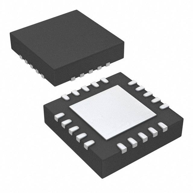
TRF3750IRGP
QFN-20
RGP
–40°C to 85°C
TRF3750
TRF3750IRGP
Tube
91
TRF3750IRGPR
QFN-20
RGP
–40°C to 85°C
TRF3750
TRF3750IRGPR
Reel
1000
PIN ASSIGNMENTS
TERMINAL
NAME
RSET
QFN(1)
NO.
TSSOP
NO.
TYPE
19
1
O
DESCRIPTION
The user needs to place an external resistor (RSET) from this pin to ground to control the
maximum charge pump current. This node’s output voltage is typically around 1 V and the
relationship between ICPOUTmax and RSET is:
+ 23.5
RSET
A 4.7-kΩ resistor placed at this pin to ground would hence provide a maximum charge pump
output current of approximately 5 mA.
I
CPOUT
CPOUTmax
20
2
O
Charge pump output. This node provides the charge pump current that ultimately controls the
external VCO.
CPGND
1
3
I
Charge pump ground
AGND
23
4
I
Analog ground
RFIN
4
5
I
Complementary input to the prescaler. For single-ended applications, bypass with a small
capacitor to ground (typically 100 pF).
RFIN
5
6
I
Input to the prescaler. To complete the PLL, this signal must come from the output of the
external VCO.
AVDD
6, 7
7
I
Analog power supply. There are two possible supply ranges: 3 V − 3.6 V and 4.5 V − 5.5 V.
This value should be the same as the DVDD. Appropriate decoupling is necessary for optimal
performance.
REFIN
8
8
I
Reference frequency input. This externally provided reference gets divided by the selectable R
divider, and is used to synthesize the desired output frequency. Typically this input is an
ac-coupled sinusoid; however, a TTL or CMOS signal can also be used.
DGND
9, 10
9
I
Digital ground
CE
11
10
I
Chip enable. Setting this pin low puts the device into power down; setting it high activates the
charge pump if the software controlled power down is also disabled.
CLOCK
12
11
I
Serial clock input. This is the input that is used to clock the serial data into the 24-bit shift
register of the device. The data is read at the rising edge of this clock.
DATA
13
12
I
Serial data input. This is the data stream that contains the data to be loaded into the shift
register. The data is loaded MSB first.
LE
14
13
I
Load enable. When this asynchronous signal is asserted high, the data existing in the shift
register get loaded onto the selected latch.
MUXOUT
15
14
O
This user-selectable output can be controlled to provide the digital or analog lock detect
signals, the divide by N RF signal or the divide by R reference. The output can also be
3-stated.
16, 17
15
I
Digital power supply. There are two possible supply ranges: 3 V − 3.6 V and 4.5 V − 5.5 V. This
value should be the same as the AVDD. Appropriate decoupling is necessary for optimal
performance.
18
16
I
Charge pump supply. This supply must be at least 1 V greater than the AVDD and DVDD and
can be as high as 8 V, accommodating a large range of possible VCOs.
DVDD
VCP
(1)
The thermal pad on the bottom of the QFN package may be tied to ground, but is not required to meet specified performance.
3
�TRF3750
www.ti.com
SLWS146B − MARCH 2004 − REVISED AUGUST 2007
ABSOLUTE MAXIMUM RATINGS
over operating free-air temperature range unless otherwise noted(1)
UNIT
Supply voltage range(2)
AVDD
−0.3 V to 6.5 V
AVDD to DVDD
−0.3 V to 0.3 V
VCP to AGND
−0.3 V to 9 V
Digital I/O voltage to DGND (DGND = 0 V)
−0.3 V to 6.5 V
Reference signal input
REFIN to DGND
RF prescaler input
RFIN, RFIN to AGND
−0.3 V to DVDD + 0.3 V
−0.3 V to 6.5 V
Continuous power dissipation
See Dissipation Rating Table
Storage temperature, TStg
−65°C to 150°C
Lead temperature 1,6 mm (1/16 inch) from case for 10 seconds
260°C
(1)
Stresses beyond those listed under “absolute maximum ratings” may cause permanent damage to the device. These are stress ratings only, and
functional operation of the device at these or any other conditions beyond those indicated under “recommended operating conditions” is not
implied. Exposure to absolute-maximum-rated conditions for extended periods may affect device reliability.
(2) All voltage values are with respect to network ground terminal.
DISSIPATION RATING TABLE
(1)
PACKAGE
TA ≤ 25°C
DERATING FACTOR(1)
ABOVE TA = 25°C
TA = 85°C
POWER RATING
16-pin TSSOP
2780 mW
22.2 mW/_C
1440 mW
20-pin QFN
2780 mW
29 mW/_C
1440 mW
This is the inverse of the junction-to-ambient thermal resistance when board mounted and with no airflow.
RECOMMENDED OPERATING CONDITIONS
AVDD = DVDD, 3.3 V range
Supply voltage
AVDD = DVDD, 5 V range
VCP
High−level input voltage, VIH
Low−level input voltage, VIL
High−level output voltage, VOH
Low−level output voltage, VOL
Operating free-air temperature, TA
4
LE DATA
LE,
DATA, CLK
CLK, CE
MUXOUT
MIN
NOM
MAX
3
3.3
3.6
V
4.5
5
5.5
V
8
V
(AVDD, DVDD) + 1
0.8 x DVDD
V
0.2 x DVDD
DVDD − 0.4
−40
UNIT
V
V
0.4
V
85
°C
�TRF3750
www.ti.com
SLWS146B − MARCH 2004 − REVISED AUGUST 2007
ELECTRICAL CHARACTERISTICS
Conditions: (AVDD = DVDD = 3.3 V or 5 V, AVDD + 1≤ VCP ≤ 8 V, RSET = 4.7 kΩ, TA = −40°C to 85°C, REFIN = 10 MHz at +5 dBm) (unless
otherwise stated)
PARAMETER
IAVDD
Supply current
IDVDD
Supply current
IVCP
Supply current
TEST CONDITIONS
MIN
TYP
AVDD = 3.3 V
10
AVDD = 5 V
13
DVDD = 3.3 V
3.5
VCP = 7 V
7.5
RFIN input frequency (RF input)
RF prescaler output frequency
−15
(1)
REFIN input frequency (reference input) (1)
4
REFIN input power level sensitivity
Charge pump max source current
ICPOUTmin
Charge pump max sink current
VTUNE
(1)
(2)
Output tuning voltage (2)
mA
2400
MHz
+5
dBm
200
MHz
200
MHz
dBm
5
PFD maximum frequency (1)
ICPOUTmax
mA
−10
REFIN input capacitance
pF
60
Measured at the output of the
external loop filter, in locked
condition
1
UNIT
mA
3
DVDD = 5 V
RFIN input power level
MAX
MHz
5
mA
−5
mA
VCP−1.1
V
Assured by design.
VTUNE range shown is for optimal spurious performance; the device can function beyond these limits.
5
�TRF3750
www.ti.com
SLWS146B − MARCH 2004 − REVISED AUGUST 2007
ELECTRICAL CHARACTERISTICS
Conditions (unless otherwise stated): AVDD = DVDD = 3.3 V or 5 V, VCP = 7 V; RSET = 4.7 kΩ, TA = 27°C, REFIN = 10 MHz at 6.5 dBm
Referenced to 50 Ω, ICPOUTmax = 5 mA, Power Down: Normal Operation; Timer Counter Control: Not used; MUXOUT Control: 3-state; Fast
Lock Mode: Disabled, PFD Polarity: Positive, Anti-backlash Pulse width: 1.5 ns, Resync/Delay: Normal (Delay=0, Resync=0), Counter
Operation: Normal, Charge Pump Output: Normal, Lock Detect Precision: 5 cycles
PARAMETER
Phase noise 110 MHz)
Reference spurs 110 MHz
Phase noise 300 MHz
Reference spurs 300 MHz
Phase noise 540 MHz
Reference spurs 540 MHz
Phase noise 836 MHz
Reference spurs 836 MHz
Phase noise 900 MHz
Phase noise 900 MHz, over temperature and supply
Reference spurs 900 MHz
Reference spurs 900 MHz, over temperature and supply
Phase noise 1750 MHz
Reference spurs 1750 MHz
Phase noise 1960 MHz
Phase noise 1960 MHz, over temperature and supply
Reference spurs 1960 MHz
Reference spurs 1960 MHz, over temperature and supply
Phase noise 2200 MHz
Reference spurs 2200 MHz
6
TEST CONDITIONS
PFD = 200 kHz, Loop Loop BW = 20 kHz,
N =550,
550 Phase noise measured at 1-kHz
1 kHz offset
spurs measured at ±PFD, ±2 x PFD
MIN
TYP
MAX
UNIT
−106
dBc/Hz
−110
dBc
−99
dBc/Hz
−110
dBc
PFD = 200 kHz, Loop Loop BW = 20 kHz,
N = 2700,
2700 Phase noise measured at 1
1-kHz
kHz
offset spurs measured at ±PFD, ±2 x PFD
−94
dBc/Hz
−90
dBc
PFD = 200 kHz, Loop Loop BW = 20 kHz,
N = 4180,
4180 Phase noise measured at 1
1-kHz
kHz
offset spurs measured at ±PFD, ±2 x PFD
−91
dBc/Hz
−100
dBc
PFD = 200 kHz, Loop Loop BW = 20 kHz,
N =1500,
1500 Phase noise measured at 1
1-kHz
kHz
offset spurs measured at ±PFD, ±2 x PFD
PFD = 200 kHz, Loop Loop BW = 20 kHz,
N = 4500
4500, Phase noise measured at 1
1−kHz
kHz
offset spurs measured at ±PFD, ±2 x PFD
−91
PFD = 200 kHz, Loop Loop BW = 20 kHz,
N = 4500,
4500 Phase noise measured at 1
1-kHz
kHz
offset spurs measured at ±PFD, ±2 x PFD
−100
dBc
−100
dBc
PFD = 200 kHz, Loop Loop BW = 20 kHz,
N = 8750
Phase noise measured at 1-kHz offset spurs
measured at ±PFD, ±2 x PFD
−84
dBc/Hz
−96
dBc
PFD = 200 kHz, Loop Loop BW = 20 kHz,
N = 9800,
9800 Phase noise measured at 1
1-kHz
kHz
offset spurs measured at ±PFD, ±2 x PFD
−84
PFD = 200 kHz, Loop Loop BW = 20 kHz,
N = 9800,
9800 Phase noise measured at 1-kHz
1 kHz
offset spurs measured at ±PFD, ±2 x PFD
−90
dBc
−90
dBc
PFD = 200 kHz, Loop Loop BW = 20 kHz,
N = 11000
11000, Phase noise measured at 1
1-kHz
kHz
offset spurs measured at ±PFD, ±2 x PFD
−83
dBc/Hz
−90
dBc
−90
−82
dBc/Hz
dBc/Hz
�TRF3750
www.ti.com
SLWS146B − MARCH 2004 − REVISED AUGUST 2007
PRODUCT TIMING CHARACTERISTICS
AVDD = DVDD = 3.3 V ±10% or 5 V ±10% , TA = −40°C to 85°C (unless otherwise stated)
PARAMETER
TEST CONDITIONS
MIN
period(1)
TYP
MAX
UNIT
t(CLK)
Clock
50
ns
tsu1
Data setup time(2)
10
ns
th
Data hold time(2)
10
ns
tw
LE pulse
width(2)
20
ns
tsu2
LE setup time(2)
10
ns
(1)
Production tested.
(2) Assured by design.
t(CLK)
CLOCK
tsu1
th
DATA
DB20 (MSB)
DB19
DB2
DB1
DB0 (LSB)
tw
LE
tsu2
Figure 1. Serial Programming Timing Diagram
7
�TRF3750
www.ti.com
SLWS146B − MARCH 2004 − REVISED AUGUST 2007
TYPICAL CHARACTERISTICS
(Conditions are based on Electrical Characteristics table on page 6, unless otherwise noted)
OUTPUT POWER
vs
FREQUENCY
−10
Reference Level = −7.4 dBm
PO − Output Power − dBc
−20
−30
−40
AVDD = DVDD = 3.3 V
ICP = 5 mA
Res. Bandwidth = 100 Hz
Video Bandwidth = 100 Hz
Average = 30
PFD = 200 kHz
Loop Loop BW = 20 kHz
−50
−60
−70
−80
−90
−40
RMS = 0.14°
PFD = 200 kHz
Loop BW = 20 kHz
−50
−60
Phase Noise − dBc/Hz
0
PHASE NOISE
vs
FREQUENCY
−110 dBc
−70
−80
−90
−100
−110
−120
−100
−130
−110
−120
−500−400 −300 −200 −100 0
−140
100
100 200 300 400 500
f − Frequency Offset from 110 MHz Carrier − kHz
1k
Figure 2. Reference Spurs
(RFOUT = 110 MHz)
PO − Output Power − dBc
−20
−30
−40
AVDD = DVDD = 3.3 V
ICP = 5 mA
Res. Bandwidth = 300 Hz
Video Bandwidth = 300 Hz
Average = 20
PFD = 200 kHz
Loop BW = 20 kHz
−50
−60
−70
−80
−90
−108 dBc
−100
−40
RMS = 0.18°
PFD = 200 kHz
Loop BW = 20 kHz
−50
−60
−70
−80
−90
−100
−110
−120
−130
−110
−120
−500−400 −300 −200 −100 0
100 200 300 400 500
f − Frequency Offset from 300 MHz Carrier − kHz
Figure 4. Reference Spurs
(RFOUT = 300 MHz)
8
1M
PHASE NOISE
vs
FREQUENCY
Phase Noise − dBc/Hz
−10
Reference Level = −5.5 dBm
100k
Figure 3. Integrated Phase Noise
(RFOUT = 110 MHz)
OUTPUT POWER
vs
FREQUENCY
0
10k
f − Frequency Offset from 110 MHz Carrier − Hz
−140
100
1k
10k
100k
f − Frequency Offset from 300 MHz Carrier − Hz
Figure 5. Integrated Phase Noise
(RFOUT = 300 MHz)
1M
�TRF3750
www.ti.com
SLWS146B − MARCH 2004 − REVISED AUGUST 2007
TYPICAL CHARACTERISTICS
OUTPUT POWER
vs
FREQUENCY
Reference Level = −5.7 dBm
PO − Output Power − dBc
−20
−30
−40
AVDD = DVDD = 3.3 V
ICP = 5 mA
Res. Bandwidth = 1 kHz
Video Bandwidth = 1 kHz
Average = 30
PFD = 200 kHz
Loop BW = 20 kHz
−50
−60
−70
−91.5 dBc
−80
−90
−40
RMS = 0.36°
PFD = 200 kHz
Loop BW = 20 kHz
−50
−60
Phase Noise − dBc/Hz
0
−10
PHASE NOISE
vs
FREQUENCY
−70
−80
−90
−100
−110
−120
−100
−130
−110
−120
−500−400 −300 −200 −100 0
−140
100
100 200 300 400 500
1k
Figure 6. Reference Spurs
(RFOUT = 540 MHz)
PO − Output Power − dBc
−20
−30
−40
AVDD = AVDD = 3.3 V
ICP = 5 mA
Res. Bandwidth = 1 kHz
Video Bandwidth = 1 kHz
Average = 30
PFD = 200 kHz
Loop BW = 20 kHz
−50
−60
−70
−80
1M
PHASE NOISE
vs
FREQUENCY
−100 dBc
−90
−40
RMS = 0.39°
PFD = 200 kHz
Loop BW = 20 kHz
−50
−60
Phase Noise − dBc/Hz
−10
Reference Level = −5.7 dBm
100k
Figure 7. Integrated Phase Noise
(RFOUT = 540 MHz)
OUTPUT POWER
vs
FREQUENCY
0
10k
f − Frequency Offset from 540 MHz Carrier − Hz
f − Frequency Offset from 540 MHz Carrier − kHz
−70
−80
−90
−100
−110
−120
−100
−130
−110
−120
−500−400 −300 −200 −100 0
100 200 300 400 500
f − Frequency Offset from 836 MHz Carrier − kHz
Figure 8. Reference Spurs
(RFOUT = 836 MHz)
−140
100
1k
10k
100k
1M
f − Frequency Offset from 836 MHz Carrier − Hz
Figure 9. Integrated Phase Noise
(RFOUT = 836 MHz)
9
�TRF3750
www.ti.com
SLWS146B − MARCH 2004 − REVISED AUGUST 2007
TYPICAL CHARACTERISTICS
OUTPUT POWER
vs
FREQUENCY
0
−30
−40
Reference Level = −5.4 dBm
−10
−20
PO − Output Power − dBc
−20
PO − Output Power − dBc
0
AVDD = DVDD = 3.3 V
ICP = 5 mA
Res. Bandwidth = 1 kHz
Video Bandwidth = 1 kHz
Average = 30
PFD = 200 kHz
Loop BW = 20 kHz
Reference Level = −5.5 dBm
−10
OUTPUT POWER
vs
FREQUENCY
−50
−60
−70
−80
−100 dBc
−90
−30
−40
−50
−60
−70
−90
−110
−120
−500−400 −300 −200 −100 0
−100
−2.5 −2.0 −1.5 −1.0 −0.5 0.0 0.5 1.0 1.5 2.0 2.5
100 200 300 400 500
f − Frequency Offset from 900 MHz Carrier − kHz
f − Frequency Offset from 900 MHz Carrier − kHz
Figure 10. Reference Spurs
(RFOUT = 900 MHz)
Figure 11. Phase Noise
(RFOUT = 900 MHz)
PHASE NOISE
vs
FREQUENCY
−40
OUTPUT POWER
vs
FREQUENCY
0
RMS = 0.40°
PFD = 200 kHz
Loop BW = 20 kHz
−50
−10
PO − Output Power − dBc
Phase Noise − dBc/Hz
Reference Level = −5.3 dBm
−20
−60
−70
−80
−90
−100
−110
−120
−30
−40
AVDD = DVDD = 3.3 V
ICP = 5 mA
Res. Bandwidth = 1 kHz
Video Bandwidth = 1 kHz
Average = 25
PFD = 200 kHz
Loop BW = 20 kHz
−50
−60
−70
−96 dBc
−80
−90
−100
−130
−110
−140
100
1k
10k
100k
f − Frequency Offset from 900 MHz Carrier − Hz
Figure 12. Integrated Phase Noise
(RFOUT = 900 MHz)
10
−93 dBc/Hz
−80
−100
AVDD = DVDD = 3.3 V
ICP = 5 mA
Res. Bandwidth = 1 Hz
Video Bandwidth = 1 Hz
Average = 30
PFD = 200 kHz
Loop BW = 20 kHz
1M
−120
−500−400 −300 −200−100 0
100 200 300 400 500
f − Frequency Offset from 1750 MHz Carrier − kHz
Figure 13. Reference Spurs
(RFOUT = 1750 MHz)
�TRF3750
www.ti.com
SLWS146B − MARCH 2004 − REVISED AUGUST 2007
TYPICAL CHARACTERISTICS
PHASE NOISE
vs
FREQUENCY
−40
OUTPUT POWER
vs
FREQUENCY
0
RMS = 0.95°
RMS
= 0.95°
PFD = 200 kHz
Loop BW = 20 kHz
−50
−20
−70
PO − Output Power − dBc
Phase Noise − dBc/Hz
−60
−80
−90
−100
−110
−120
−30
−40
−50
−60
−70
−92 dBc
−80
−90
−100
−130
−110
−140
100
1k
10k
100k
−120
−500−400 −300 −200−100 0
1M
f − Frequency Offset from 1750 MHz Carrier − Hz
PO − Output Power − dBc
−20
−30
OUTPUT POWER
vs
FREQUENCY
Reference Level = −6.7 dBm
AVDD = DVDD = 3.3 V
ICP = 5 mA
Res. Bandwidth = 1 Hz
Video Bandwidth = 1 Hz
Average = 30
PFD = 200 kHz
Loop BW = 20 kHz
−40
−50
−60
−70
Figure 15. Reference Spurs
(RFOUT = 1960 MHz)
−84 dBc/Hz
−80
PHASE NOISE
vs
FREQUENCY
−40
RMS = 0.98°
PFD = 200 kHz
Loop BW = 20 kHz
−50
−60
Phase Noise − dBc/Hz
−10
100 200 300 400 500
f − Frequency Offset from 1960 MHz Carrier − kHz
Figure 14. Phase Noise
(RFOUT = 1750 MHz)
0
AVDD = DVDD = 3.3 V
ICP = 5 mA
Res. Bandwidth = 1 kHz
Video Bandwidth = 1 kHz
Average = 30
PFD = 200 kHz
Loop BW = 20 kHz
Reference Level = −6.9 dBm
−10
−70
−80
−90
−100
−110
−120
−90
−130
−100
−2.5 −2.0 −1.5 −1.0 −0.5 0.0 0.5 1.0 1.5 2.0 2.5
f − Frequency Offset from 1960 MHz Carrier − kHz
Figure 16. Phase Noise
(RFOUT = 1960 MHz)
−140
100
1k
10k
100k
1M
f − Frequency Offset from 1960 MHz Carrier − Hz
Figure 17. Integrated Phase Noise
(RFOUT = 1960 MHz)
11
�TRF3750
www.ti.com
SLWS146B − MARCH 2004 − REVISED AUGUST 2007
TYPICAL CHARACTERISTICS
OUTPUT POWER
vs
FREQUENCY
0
−30
−40
−60
−50
−60
−70
RMS = 0.98°
PFD = 200 kHz
Loop BW = 20 kHz
−50
Phase Noise − dBc/Hz
−20
PO − Output Power − dBc
−40
AVDD = AVDD = 3.3 V
ICP = 5 mA
Res. Bandwidth = 1 kHz
Video Bandwidth = 1 kHz
Average = 25
PFD = 200 kHz
Loop BW = 20 kHz
Reference Level = −7.0 dBm
−10
PHASE NOISE
vs
FREQUENCY
−90 dBc
−80
−90
−70
−80
−90
−100
−110
−120
−100
−130
−110
−120
−500−400 −300 −200 −100 0
−140
100
100 200 300 400 500
1k
Figure 18. Reference Spurs
(RFOUT = 2200 MHz)
−90
VCP = 7 V
VCP = 7 V
−95
1960 MHz, AVDD = DVDD = 3.3 V
Reference Spur Level − dBc
−80
Phase Noise − dBc/Hz
1M
REFERENCE SPUR LEVEL
vs
FREE-AIR TEMPERATURE
−75
−85
1960 MHz, AVDD = DVDD = 5 V
900 MHz, AVDD = DVDD = 5 V
−90
900 MHz, AVDD = DVDD = 3.3 V
−95
1960 MHz, AVDD = DVDD = 3.3 V
1960 MHz, AVDD = DVDD = 5 V
−100
−105
900 MHz, AVDD = DVDD = 5 V
−110
900 MHz, AVDD = DVDD = 3.3 V
−115
−20
0
20
40
60
TA − Free-Air Temperature − °C
Figure 20.
12
100k
Figure 19. Integrated Phase Noise
(RFOUT = 2200 MHz)
PHASE NOISE
vs
FREE-AIR TEMPERATURE
−100
−40
10k
f − Frequency Offset from 2200 MHz Carrier − Hz
f − Frequency Offset from 2200 MHz Carrier − kHz
80
100
−120
−40
−20
0
20
40
60
TA − Free-Air Temperature − °C
Figure 21.
80
100
�TRF3750
www.ti.com
SLWS146B − MARCH 2004 − REVISED AUGUST 2007
TYPICAL CHARACTERISTICS
REFERENCE SPURS
vs
VTUNE
CURRENT
vs
PRESCALER SETTING
0
12
IAVDD
−10
−30
−40
I − Current − mA
Reference Spurs − dBc
IDVDD
10
−20
−50
−60
−70
VCP = 7 V
−80
8
6
4
VCP = 5 V
−90
2
−100
−110
1
2
3
VTUNE − V
Figure 22.
4
0
0
8
16
24
32
40
48
56
64
Prescaler Setting
Figure 23.
13
�TRF3750
www.ti.com
SLWS146B − MARCH 2004 − REVISED AUGUST 2007
Table 1. S11 Data for RFIN Buffer
14
FREQ (Hz)
MAG(S11)
PHASE(S11)
300M
849.388m
1.07722
344M
848.792m
1.02901
388M
848.317m
998.914m
432M
847.916m
981.324m
476M
847.565m
972.594m
520M
847.25m
970.294m
564M
846.962m
972.761m
608M
846.696m
978.834m
652M
846.448m
987.691m
696M
846.217m
998.737m
740M
846m
1.01154
784M
845.797m
1.02578
828M
845.605m
1.04122
872M
845.425m
1.05768
916M
845.255m
1.07502
960M
845.094m
1.09312
1.004G
844.943m
1.11191
1.048G
844.8m
1.13131
1.092G
844.664m
1.15127
1.136G
844.535m
1.17173
1.18G
844.413m
1.19267
1.224G
844.296m
1.21403
1.268G
844.185m
1.2358
1.312G
844.079m
1.25795
1.356G
843.978m
1.28045
1.4G
843.88m
1.30327
1.444G
843.787m
1.32641
1.488G
843.697m
1.34985
1.532G
843.61m
1.37355
1.576G
843.526m
1.39752
1.62G
843.444m
1.42174
1.664G
843.365m
1.44619
1.708G
843.288m
1.47086
1.752G
843.214m
1.49574
1.796G
843.14m
1.52082
1.84G
843.069m
1.54608
1.884G
842.999m
1.57152
1.928G
842.93m
1.59713
1.972G
842.862m
1.62291
2.016G
842.796m
1.64883
2.06G
842.73m
1.6749
2.104G
842.665m
1.70111
2.148G
842.601m
1.72744
2.192G
842.537m
1.7539
2.236G
842.474m
1.78048
2.28G
842.411m
1.80717
2.324G
842.349m
1.83397
2.368G
842.287m
1.86086
2.412G
842.225m
1.88786
2.456G
842.164m
1.91494
2.5G
842.103m
1.94211
�TRF3750
www.ti.com
SLWS146B − MARCH 2004 − REVISED AUGUST 2007
FUNCTIONAL DESCRIPTION
REFIN Stage
This input typically comes from an external oscillator and is the reference used to synthesize the desired
frequency on the output of the complete PLL. The equivalent schematic of this section is given in Figure 24.
The output of this section goes to the R divider, so that the desired PFD frequency can be implemented.
PDZ
PDZ
R
PD
PD
Figure 24. REFIN Stage
RFIN Stage
Figure 25 shows the input stage of the TRF3750. This is where the output of the external VCO is fed back to the
synthesizer. The RFIN signal subsequently feeds the prescaler section.
AVDD
RFIN
VBIAS
RFINB
Figure 25. RFIN Stage
Prescaler Stage
This stage divides down the RFIN frequency before the A and B counters. This is a dual-modulus prescaler and the
user can select any of the following settings: 8/9, 16/17, 32/33, and 64/65.
A and B Counter Stage
The TRF3750 includes a 6-bit A counter and a 13-bit B counter that operate on the output of the prescaler. The A
counter can take values from 0 to 63, while the B counter can take values from 3 to 8191. Also, the value for the B
counter has to be greater than or equal to the value for the A counter. These are CMOS devices, and can easily
operate up to 200 MHz. The selection of the prescaler needs to be such that the resultant frequency does not exceed
the rated 200-MHz threshold.
R Divider
The output of the REFIN stage is fed into the R divider stage. The 14-bit R divider allows the input reference frequency
to be divided down to produce the reference clock to the phase frequency detector (PFD). Division ratios from 1 to
16,383 are allowed.
15
�TRF3750
www.ti.com
SLWS146B − MARCH 2004 − REVISED AUGUST 2007
Phase Frequency Detector (PFD) and Charge Pump Stage
The outputs of the R divider and the N counter (please see pulse swallow section) are fed into the PFD stage, where
the two signals are compared in frequency and phase. The TRF3750 features an anti-backlash pulse, whose width
is controllable by the user, in order to optimize phase and spurious performance. The PFD feeds the charge pump,
which is the final output of the TRF3750. The charge pump output pulses need to be fed into an external loop filter,
which eventually produces the tuning voltage needed to control the external VCO to the desired frequency.
Pulse Swallow/Frequency Synthesis
The different stages of the TRF3750 enable the user to synthesize a large range of frequencies at the output of a
complete PLL. For a given reference frequency (fREFIN), the user’s choice of the R divider yields the PFD frequency
(fPFD), which is the step by which the resultant output frequency can be incremented or decremented. The choice
of prescaler, and A and B counters yields the output frequency at the external VCO (RFOUT) as shown below.
RFOUT = fPFD x N = (fREFIN / R) x (A + P x B)
MUXOUT Stage
The TRF3750 features a multiplexer that allows programmable access to several signals. Table 5 and Table 6 show
the truth tables. Some of the different signals available are detailed below.
Digital Lock Detect
This is an active high digital output that indicates when the device has achieved lock. The user can choose between
two precision settings for the lock detection, through the reference counter latch. A 0 on the lock detect precision
means that the digital lock detect output goes high only if three contiguous cycles of the PFD have an error of less
than 15 ns. A 1 would require five contiguous cycles (a more stringent condition). Any error of greater than 25 ns,
even on one cycle, would produce a 0 in the digital lock detect signal, indicating loss of lock.
Analog Lock Detect
Selecting the analog lock detect option at the output of the output multiplexer requires an external pull-up resistor
(≈10 kΩ) to be placed on the output (MUXOUT, pin 14).
Fastlock Mode
The TRF3750 features two Fastlock Modes, which the user may select depending on the particular application.
There are two separate charge pump current settings (1 and 2) that can be programmed, and the Fastlock
Modes, when activated, enable the device to quickly switch from current setting 1 to current setting 2. The two
Fastlock Modes (1 and 2) differ in the way the device reverts back to current setting 1. In normal (steady-state)
operation, current setting 1 is used. For transient situations such as frequency jumps, current setting 2 can be
used.
Fastlock Mode 1
As soon as Fastlock Mode 1 is entered, the charge pump current is switched to the preprogrammed setting 2
and stays there until the charge pump gain programming bit is set to 0 in the N counter latch. This way, the user
has immediate software control of the transition between charge pump setting 1 and 2.
Fastlock Mode 2
As soon as Fastlock Mode 2 is entered, the charge pump current is switched to the preprogrammed setting 2
and stays there until the timer counter has expired. The timer counter is programmed by the user and counts
how many PFD cycles the device spends in current setting 2 in Fastlock Mode 2. The number of timer cycles
can be set in increments of four cycles in the range of 3 to 63. When the counter has expired, the device returns
to normal operation (fastlock disabled and charge pump current setting 1). This way no extra programming is
needed in order for the device to exit fastlock.
3-Wire Serial Programming
The TRF3750 features an industry-standard 3-wire serial interface that controls an internal 24-bit shift register.
There are a total of 3 signals that need to be applied: the clock (CLK, pin 11), the serial data (DATA, pin 12)
and the load enable (LE, pin13). The DATA (DB0−DB23) is loaded MSB first and is read on the rising edge of
the CLK. The LE signal is asynchronous to the clock and at its rising edge the DATA gets loaded onto the
16
�TRF3750
www.ti.com
SLWS146B − MARCH 2004 − REVISED AUGUST 2007
selected latch. The last two bits of the serial data (DB0 and DB1) are the bits that control one of the four available
latches (R counter latch, N counter latch, function latch, and initialization latch). The truth table for selecting
the appropriate latch is shown in Table 2.
Table 2. Latch Selection Truth Table
DB1 (C2)
DB0 (C1)
SELECTED DATA LATCH
0
0
R counter
0
1
N counter
1
0
Function
1
1
Initialization
17
�TRF3750
www.ti.com
SLWS146B − MARCH 2004 − REVISED AUGUST 2007
Latch Description
Table 3. R Counter Latch
Reserved
Lock
Detect
Precision
DB23 DB22 DB21
DB20
X†
DLY
SYNC
LDP
Test
Mode
Bits
Anti
Backlash
Pulse Width
DB19 DB18 DB17 DB16 DB15 DB14 DB13 DB12 DB11 DB10
T2
T1
ABP2 ABP1
Control
Bits
14-Bit Reference Counter, R
R14
R13
R12
R11
R10
R9
DB9
DB8
DB7
DB6
DB5
DB4
DB3
DB2
DB1
DB0
R8
R7
R6
R5
R4
R3
R2
R1
C2(0)
C1(0)
Set to 00
AntiBacklash Pulse Width
0
0
3 ns
0
1
1.5 ns
1
0
6 ns
1
1
3 ns
LDP
Operation
0
3 contiguous cycles of phase delay < 15 ns
must occur before Lock Detect is set.
1
5 contiguous cycles of phase delay < 15 ns
must occur before Lock Detect is set.
SYNC
0
0
Normal operation
0
1
Prescaler resynchronized with nondelayed
form of RF input
1
0
Normal operation
1
Prescaler resynchronized with delayed form
of RF input
X = Don’t Care
18
ABP1
DLY
1
†
ABP2
Operation
R14
R13
R12
•••
R3
R2
R1
Divide
Ratio
0
0
0
•••
0
0
1
1
0
0
0
•••
0
1
0
2
0
0
0
•••
0
1
1
3
0
0
0
•••
1
0
0
4
•
•
•
•••
•
•
•
•
•
•
•
•••
•
•
•
•
•
•
•
•••
•
•
•
•
1
1
1
•••
1
0
0
16380
1
1
1
•••
1
0
1
16381
1
1
1
•••
1
1
0
16382
1
1
1
•••
1
1
1
16383
�TRF3750
www.ti.com
SLWS146B − MARCH 2004 − REVISED AUGUST 2007
Latch Description (Continued)
Table 4. AB Counter Latch
Reserved
CP
Gain
DB23 DB22
DB21
X†
X†
G1
13-Bit B Counter
DB20 DB19 DB18 DB17 DB16 DB15 DB14 DB13 DB12 DB11 DB10
B13
B12
B11
B10
B9
B8
Control
Bits
6-Bit A Counter
B7
B6
B5
B4
DB9
DB8
DB7
DB6
DB5
DB4
DB3
DB2
DB1
DB0
B2
B1
A6
A5
A4
A3
A2
A1
C2(0)
C1(1)
B3
B≥A
B12
B11
•••
B3
B2
B1
B Counter
Divide Ratio
A6
A5
•••
A2
A1
A Counter
0
0
0
•••
0
0
0
N/A
0
0
•••
0
0
0
0
0
0
•••
0
0
1
N/A
0
0
•••
0
1
1
0
0
0
•••
0
1
0
N/A
0
0
•••
1
0
2
0
0
0
•••
0
1
1
3
0
0
•••
1
1
3
0
0
0
•••
1
0
0
4
•
•
•••
•
•
•
•
•
•
•••
•
•
•
•
•
•
•••
•
•
•
•
•
•
•••
•
•
•
•
•
•
•••
•
•
•
•
•
•
•••
•
•
•
•
1
1
•••
0
0
60
1
1
1
•••
0
0
0
8188
1
1
•••
0
1
61
1
1
1
•••
0
0
1
8189
1
1
•••
1
0
62
1
1
1
•••
1
1
0
8190
1
1
•••
1
1
63
1
1
1
•••
1
1
1
8191
F4 (Function Latch D89)
Fastlock Enable
CP
Gain
Charge Pump Current Setting Operation
0
0
Current setting 1 is always used
0
1
Current setting 2 is always used
1
0
1
†
B13
1
Current setting 1 used
Current setting 2 is used until fastlock mode exits (returns to current setting 1)
X = Don’t Care
19
�TRF3750
www.ti.com
SLWS146B − MARCH 2004 − REVISED AUGUST 2007
Latch Description (Continued)
Table 5. Function Latch
Prescaler
Value
Power
Down
2
DB23 DB22
DB21
DB20 DB19 DB18 DB17 DB16 DB15 DB14 DB13 DB12 DB11
PD2
CP16 CP15 CP14 CP13 CP12 CP11 TC4
P2
P1
Current
Setting 2
Current
Setting 1
CP16 CP15 CP14
CP13 CP12 CP11
†
Reserved
DB10
DB9
DB8
DB7
F5
F4
F3
X{
MUXOUT
Control
Power
Down
1
Counter
Reset
Control
Bits
DB6 DB5 DB4
DB3
DB2
DB1 DB0
PD1
F1
C2(1) C1(0)
M3
M2
F1
4.7 kΩ
10 kΩ
Normal
1
R, A, B counters
reset
M2
M1
Output
0
0
0
3-State output
0
0
1
Digital lock detect
0
1
0
N divider output
0
1
1
DVDD
1
0
0
R divider output
1
0
1
Analog lock detect
0.29
0
0
1
2.18
1.25
0.59
0
1
0
3.26
1.88
0.88
F3
Charge Pump Output
0
1
1
4.35
2.50
1.76
0
Normal
M3
1
0
0
5.44
3.13
1.47
1
Tri-State
1
0
1
6.53
3.75
1.76
1
1
0
7.62
4.38
2.06
1
1
1
8.70
5.00
2.35
8/9
0
1
16/17
1
0
32/33
1
1
64/65
F4
F5
Fastlock Mode
0
X†
Fastlock disable
1
0
Fastlock mode 1
1
1
Fastlock mode 2
Counter Operation
0
0.63
0
M1
ICPOUTmax (mA)
2.7 kΩ
1.09
0
20
CP
Tri-State
0
Prescaler Value
TC4
TC3
TC2
TC1
Timeout
(PFD Cycles)
1
1
0
Serial data output
0
0
0
0
3
1
1
1
DGND
0
0
0
1
7
0
0
1
0
11
0
0
1
1
15
0
1
0
0
19
0
1
0
1
23
Mode
0
1
1
0
27
0
1
1
1
31
1
0
0
0
35
1
0
0
1
39
1
0
1
0
43
1
0
1
1
47
1
1
0
0
51
1
1
0
0
55
1
1
1
0
59
1
1
1
1
63
0
X†
X†
Asynchronous power down
1
X†
0
Normal operation
1
0
1
Asynchronous power down
1
1
1
Synchronous power down
X = Don’t Care
TC1
Fastlock
Enable
0
P1
PD2 PD1
TC3 TC2
Fastlock
Mode
0
P2
CE
(Pin 10)
Timer Counter Control
�TRF3750
www.ti.com
SLWS146B − MARCH 2004 − REVISED AUGUST 2007
Latch Description (Continued)
Table 6. Initialization Latch
Prescaler
Value
Power
Down
2
DB23 DB22
DB21
DB20 DB19 DB18 DB17 DB16 DB15 DB14 DB13 DB12 DB11
PD2
CP16 CP15 CP14 CP13 CP12 CP11 TC4
P2
P1
Current
Setting 2
Current
Setting 1
†
TC1
Fastlock
Enable
CP
3-State
DB10
DB9
DB8
DB7
F5
F4
F3
X{
Reserved
MUXOUT
Control
Power
Down
1
Counter
Reset
Control
Bits
DB6 DB5 DB4
DB3
DB2
DB1 DB0
PD1
F1
C2(1) C1(1)
M3
M2
M1
2.7 kΩ
4.7 kΩ
10 kΩ
F1
Counter Operation
0
Normal
1
R, A, B counters
reset
0
0
0
1.09
0.63
0.29
0
0
1
2.18
1.25
0.59
0
1
0
3.26
1.88
0.88
F3
Charge Pump Output
0
1
1
4.35
2.50
1.76
0
Normal
M3
M2
M1
Output
1
0
0
5.44
3.13
1.47
1
3-State
0
0
0
3-State output
1
0
1
6.53
3.75
1.76
0
0
1
Digital lock detect
1
1
0
7.62
4.38
2.06
0
1
0
N divider output
1
1
1
8.70
5.00
2.35
0
1
1
DVDD
1
0
0
R divider output
P2
P1
Prescaler Value
0
0
8/9
0
1
16/17
1
0
32/33
1
1
64/65
CE
(Pin 10)
TC3 TC2
Fastlock
Mode
ICPOUTm,ax (mA)
CP16 CP15 CP14
CP13 CP12 CP11
Timer Counter Control
F4
F5
Fastlock Mode
0
X
Fastlock disable
1
0
Fastlock mode 1
1
1
Fastlock mode 2
TC4
TC3
TC2
TC1
Timeout
(PFD Cycles)
0
0
0
0
3
0
0
0
1
7
0
0
1
0
11
0
0
1
1
15
0
1
0
0
19
0
1
0
1
23
PD2
PD1
Mode
0
1
1
0
27
0
X
X
Asynchronous power down
0
1
1
1
31
1
X
0
Normal operation
1
0
0
0
35
1
0
1
Asynchronous power down
1
0
0
1
39
1
1
1
Synchronous power down
1
0
1
0
43
1
0
1
1
47
1
1
0
0
51
1
1
0
0
55
1
1
1
0
59
1
1
1
1
63
1
0
1
Analog lock detect
1
1
0
Serial data output
1
1
1
DGND
X = Don’t Care
21
�TRF3750
www.ti.com
SLWS146B − MARCH 2004 − REVISED AUGUST 2007
R Counter Latch
By selecting (0,0) for the control bits DB0 and DB1, the R counter latch is selected. Table 7 shows the setup
of the R counter latch.
Reserved
Table 7. R Counter Latch
DLY SYNC
DB23 DB22 DB21
X
DLY SYNC
Lock
Detect
Precision
DB20
LDP
Test
Mode Bits
Anti
Backlash
Width
Control
Bits
14-Bit Reference Counter; R
DB19 DB18 DB17 DB16 DB15 DB14 DB13 DB12 DB11 DB10 DB9 DB8 DB7 DB6 DB5 DB4 DB3 DB2 DB1
T2
T1
ABP2 ABP1 R14
R13
R12
R11
R10
R9
R8
R7
R6
R5
R4
R3
R2
DB0
R1 C2(0) C1(0)
R Value
This latch is used primarily to select the R divider for the input reference signal (REFIN). DB2 through DB15
are used to select the chosen value for the 14-bit counter. DB2 is the LSB and DB15 the MSB.
Anti-backlash Pulse
DB16 and DB17 can be used to select the width of the anti-backlash pulse in the PFD. In any PFD
implementation, there is an inherent risk of backlash, a phenomenon that can occur when the device is almost
in lock. In order to ensure that there are always pulses coming out of the charge pump and that therefore the
VCO cannot drift out of lock, the TRF3750 employs an anti-backlash pulse. The user can select the width of
the anti-backlash pulse; the values allowed are 1.5 ns, 3 ns, and 6 ns.
Lock Detect Precision
Setting DB20 of the R counter latch to 0 results in a precision of three cycles for the lock detect, while setting
it to 1 results in a precision of five cycles.
Sync / Delay
DB21−22 control the sync/delay operation of the device. If DB21 is 0, then the device is in normal operation.
Assuming DB21 is set to 1, setting DB22 to 0 utilizes a non-delayed form of the RF signal for the
resynchronization of the prescaler output, whereas setting DB22 to 1 utilizes a delayed form.
Reserved Bits
Bits DB18, DB19 and DB23 of the R counter latch are reserved. It is recommended to keep those bits 0 for
normal operation.
N Counter Latch
Setting (DB1, DB0) = (0,1) for the latch control bits selects the N counter latch. Table 8 shows the setup of the
N counter latch.
Table 8. N Counter Latch
CP
Reserved Gain
13-Bit B Counter
6-Bit B Counter
Control
Bits l
DB23 DB22 DB21 DB20 DB19 DB18 DB17 DB16 DB15 DB14 DB13 DB12 DB11 DB10 DB9 DB8 DB7 DB6 DB5 DB4 DB3 DB2 DB1 DB0
X
X
G1 B13 B12 B11 D10 B9
B8
B7
B6
B5
B4
B3 B2 B1 A6 A5 A4 A3 A2 A1 C2(0) C1(0)
A Counter
The 6 bits DB2−DB7 control the value of the A counter. The valid range is from 0 to 63. For example,
programming (DB7, DB6, DB5, DB4, DB3,DB2) = (0,0,0,0,1,0) results in a value of 2 for the A counter.
B Counter
The 13 bits DB8−DB20 of the N counter latch control the value of the B counter. The valid range is from 3 to
8191. For example, (DB20, DB19, …, DB10, DB9, DB8) = (0, 0, 0, 0, 0, 0, 0, 0, 0, 0, 1, 0, 0) results in a value
of 4 for the B counter.
Charge Pump Gain
DB21 of the N counter latch determines when the TRF3750 enters Fastlock Mode. When this bit is 1, the device
switches into fastlock and when this bit is 0, the device exits fastlock (fastlock mode 1).
22
�TRF3750
www.ti.com
SLWS146B − MARCH 2004 − REVISED AUGUST 2007
Reserved Bits
Bits DB22−DB23 of the N counter latch are reserved and can be treated as don’t cares by the user.
Function Latch
Table 9 depicts the function latch. By selecting (0,1) for the control bits DB0 and DB1, the function latch is
selected.
Table 9. Function Latch
Power
CP
Prescaler Power
MUXOUT
Current
Counter Control
Timer Counter
Fasklock Fasklock
Current
Down
Down
Tri− Reserved
Value
Control
Bits
Setting 2
Reset
Control
Mode
Enable
Setting
1
2
1
State
DB23 DB22 DB21 DB20 DB19 DB18 DB17 DB16 DB15 DB14 DB13 DB12 DB11 DB10
DB9
DB8 DB7
DB6 DB5 DB4 DB3
DB2
DB1 DB0
P2
P1 PD2 CPI6 CPI5 CPI4 CPI3 CPI2 CPI1 TC4 TC3 TC2 TC1
F5
F4
F3
M3
M2
M1
PD1
F1
C2(1) C1(0)
X
Counter Reset Bit
When this bit is set to 1, all the counters in the PLL are reset. This includes the R, A, and B counters. In a typical
application, this bit should be set to 0.
Power Down
The complete power down functionality of the TRF3750 is controlled in software by the two bits DB3 and DB21
in the function latch and in hardware by the external pin CE (pin 10). When the TRF3750 enters the power down
state, the power consumption is lowered, the charge pump is 3-stated, but the registers are still operational
enabling programming of the device. The hardware power down (CE set to 0) is immediate and asynchronous.
Assuming that CE is set to 1, the two bits can select between the software power down options available. Setting
DB3 to 0 enables normal operation of the PLL. When (DB21, DB3) = (0,1), then the asynchronous power down
is selected, which means that the device powers down as soon as the programming is read. When (DB21, DB3)
= (1,1), then the synchronous power down is enabled. In this mode, the device enters power down on the next
cycle of the charge pump. This is a more controlled power down, as it avoids potential transients or erroneous
output frequencies.
MUXOUT
Bits DB4, DB5, and DB6 determine what signal appears at the output of the internal multiplexer, as described
in Table 5. For example, the most widely used output signal on this pin would be the digital lock detect signal,
which goes high when lock has been achieved. In order to program this mode, the user has to set (DB4, DB5,
DB6) = (1,0,0).
Charge Pump 3-state
DB8 of the function latch can set the output of the charge pump in a 3-state mode, if set to 1. Normal operation
of the device is attained when this bit is 0.
Fastlock Enable and Mode
Setting DB9 of the function latch to 1 enables the Fastlock Mode, whereas setting it to 0 deactivates this feature
altogether. Assuming that DB9 is 1, DB10 selects between the two possible Fastlock Modes: Fastlock Mode
1 is selected when DB10 is 0, whereas Fastlock Mode 2 is selected when DB10 is 1. The device actually enters
fastlock when the charge pump gain bit in the N counter latch (DB21) is set to 1. Once in Fastlock Mode 1, the
device switches back when DB21 of the N counter latch is set to 0. Conversely, once in Fastlock Mode 2, the
device switches back after the timeout condition has been reached, at which point DB21 of the N counter latch
is automatically set to 0.
Timer Counter Control
DB11−DB14 of the function latch control the timer counter, in case the Fastlock Mode 2 was selected. These
four bits give the user the capability to program the number of PFD cycles that elapse before the device exits
the Fastlock Mode. Valid values for this are 3 to 63, in steps of 4 cycles. For example, programming (DB14,
DB13, DB12, DB11) = (0,0,1,0) results in 11 cycles before the Fastlock Mode times out.
Current Settings 1 and 2
DB15−DB17 control the maximum charge pump current setting 1, while DB18−20 control current setting 2. The
actual value of the maximum charge pump current will be dictated by the resistor placed outside on RSET (pin1).
23
�TRF3750
www.ti.com
SLWS146B − MARCH 2004 − REVISED AUGUST 2007
Prescaler Selection
DB22−DB23 of the function latch controls the prescaler value for the device. There are four possible settings
(9/9, 16/17, 32/33, 64/65). For example, setting (DB23, DB22) = (1,0) results in a prescaler choice of 32/33.
Initialization Latch / Programming After Power Up
Setting (DB1, DB0) = (1,1) selects the initialization latch. The make-up and programming of the initialization
latch is identical to that of the function latch. The difference here is that this latch can be used in order to program
the device at power up. When the initialization latch is programmed, an internal reset occurs at all the counters
(R, A, B) who become ready to get loaded, assuring that the next time data is loaded for the A and B counters
the device begins counting efficiently. Subsequent programming of the A and B counters will not, however,
cause this internal pulse to recur. This pulse is also used to gate the synchronous power down when that mode
is engaged. As soon as the device exits power down, the counting resumes promptly.
Alternate Ways of Programming After Power Up
In addition to the method of using the initialization latch described above, the user can also utilize the CE pin
to achieve initialization. Since the CE does not halt the operation of the serial port, the user can preprogram
the counters and as soon as the device is enabled, the counters operate and the device reaches a steady-state
and functions normally.
A third option in power up is the counter reset method. The function latch is programmed with the desired data,
and in addition DB2 (the counter reset bit) is set to 1. The R counter latch is programmed next, followed by the
N counter latch. Finally, the function latch is programmed again, but this time with a 0 in the bit DB2, disabling
the counter reset. The charge pump is 3-stated during the reset, but the synchronous power down is not
triggered.
Prescaler Resynchronization
DB22 and DB21 of the R counter latch are used to control the delay (DLY) and resynchronization (SYNC)
functions of the device. If SYNC is set to 1, then the output of the prescaler is resynchronized with the RF input.
In addition, if DLY is also 1, the output of the prescaler gets resynchronized with a delayed form of the RF input
signal. In either case, taking the SYNC to 0 reverts the device to normal operation.
The use of the SYNC and DLY functionality can improve the device’s phase noise performance by a few dBs.
It is, however, susceptible to potential malfunction, in case the chosen edge of the RF input coincides with the
prescaler. This phenomenon may be mitigated by using the DLY function, but is nonetheless unpredictable and
care should be applied, as fluctuations in temperature, supply and frequency can alter the point at which the
feature fails to operate. The normal operation of the device calls for both DLY and SYNC to be set to 0, which
is the way the TRF3750 has been characterized.
24
�TRF3750
www.ti.com
SLWS146B − MARCH 2004 − REVISED AUGUST 2007
APPLICATION INFORMATION
SYNTHESIZING A SELECTED FREQUENCY
The TRF3750 is an integer-N PLL synthesizer, and because of its flexibility (14-bit R, 6-bit A, 13-bit B counter,
and dual modulus prescaler), is ideal for synthesizing virtually any desired frequency. Let us assume that we
need to synthesize a 900-MHz local oscillator, with spacing capability (minimum frequency increment) of 200
kHz, as in a typical GSM application. The choice of the external reference oscillator to be used is beyond the
scope of this section, but assuming that a 10-MHz reference is selected, we calculate the settings that yield
the desired output frequency and channel spacing. There is usually more than one solution to a specific set of
conditions, so below is one way of achieving the desired result.
First, select the appropriate R counter value. Since a channel spacing of 200 kHz is desired, the PFD can also
be set to 200 kHz. Calculate the R value through R = REFIN/PFD = 10 MHz / 200 kHz = 50. Assume a prescaler
value of 8/9 is selected. This is a valid choice, since the prescaler output will be well within the 200-MHz limit
(900 MHz / 8 = 112.5 MHz). Select the appropriate A and B counter values. We know that RFOUT = fPFD x N
= (fREFIN / R) x (A + P x B). Therefore, we need to solve the following equation:
900 MHz = 200 kHz x (A + 8 x B)
Clearly there are many solutions to this single equation with two unknowns; there are some basic constraints
on the solution, since 3 ≤ B ≤ 8191, and also B ≥ A. So, if we pick A = 4, solving the equation yields B = 562.
Thus, one complete solution would be to choose: R = 50, A = 4, B = 562, and P = 8/9, resulting in the desired
N = 4500.
The GUI software accompanying the evaluation board of the TRF3750 includes an easy Parameter Selection
Assistant that can directly propose appropriate values for all the counters given the user’s requirements. In
addition, the software can configure all the possible settings of the TRF3750 and can output the data stream
required, so that the user has a reference when programming the serial port.
To complete the example, the serial port has to be programmed in order for the correct frequency to appear
at the output of the complete PLL. Assuming that the user wanted to program the same modes as used in the
RF Performance Specifications section, a possible sequence of serial data going into the device could be the
one listed below for the three different latches (note that the initialization latch is not used in this example):
Table 10. R Counter Latch Programming Example
DB
23
DB
22
DB
21
DB
20
DB
19
DB
18
DB
17
DB
16
DB
15
DB
14
DB
13
DB
12
DB
11
DB
10
0
0
0
1
0
0
0
1
0
0
0
0
0
0
DB9 DB8 DB7 DB6 DB5 DB4 DB3 DB2 DB1 DB0
0
0
1
1
0
0
1
0
0
0
Table 11. N Counter Latch Programming Example
DB
23
DB
22
DB
21
DB
20
DB
19
DB
18
DB
17
DB
16
DB
15
DB
14
DB
13
DB
12
DB
11
DB
10
0
0
0
0
0
0
1
0
0
0
1
1
0
0
DB9 DB8 DB7 DB6 DB5 DB4 DB3 DB2 DB1 DB0
1
0
0
0
0
1
0
0
0
1
Table 12. Function Latch Programming Example
DB
23
DB
22
DB
21
DB
20
DB
19
DB
18
DB
17
DB
16
DB
15
DB
14
DB
13
DB
12
DB
11
DB
10
0
0
0
1
1
1
1
1
1
0
0
0
1
0
DB9 DB8 DB7 DB6 DB5 DB4 DB3 DB2 DB1 DB0
0
0
1
0
0
1
0
0
1
0
25
�TRF3750
www.ti.com
SLWS146B − MARCH 2004 − REVISED AUGUST 2007
Building a Complete PLL Using the TRF3750
This application of the TRF3750 is just one of many possible ways in which a wireless infrastructure transmitter
LO can be implemented for GSM applications and beyond.
Supplies/Decoupling
Appropriate decoupling is important in ensuring optimum noise performance of the device. Ideally, the AVDD
and DVDD supplies should be separated through a ferrite and be at the same potential. A larger capacitor, in
the order of a 10 µF, should be placed in the supply chain, followed by a couple of small value decoupling
capacitors very close to the device’s supply pins. Typical values are 0.1 µF and 10 pF. The decoupling capacitors
should not be shared and should be chosen to have low ESR. The VCP supply needs to be at least 1 V greater
than the AVDD and DVDD supplies and similar decoupling should be applied.
Reference
A large range of frequencies can be used for the reference input. In this example, an external TCXO of 10 MHz
is used to provide the stable reference frequency for the REFIN pin of the device. The quality of the reference
oscillator is important, and its phase noise needs to be significantly lower than what is expected of the entire
loop as it does not get attenuated in the loop. Typically, such devices do not require 50-Ω terminations and can
be taken into the PLL ac coupled. The TRF3750 has a large range of power levels that it can accept at the REFIN
input; however stronger signals result typically in better phase noise performance. Values of +5 dBms (referred
to 50 Ω) should yield excellent performance. The TRF3750 is compatible with most commercially available
oscillators.
VCO Selection
Plenty of VCOs exist in the market that can cover the frequency range of all wireless applications today. One
clear advantage of the TRF3750 is that it features an extended charge pump supply, allowing interface to VCOs
with larger tuning ranges. VCP can be as high as 8 V, which implies that VCOs with tuning voltage ranges of
7 V can easily be accommodated. In closing the loop with the VCO, it is important to ensure that proper
termination is observed, especially in the higher range of frequency operation. A standard resistive splitter
implementation works well, where each of the three Rs in the classic T connection assume the value of 16.6 Ω.
In other cases where impedance matching is less critical than getting maximum power out of the whole PLL
loop, the user may decide to leave the resistors out and just tap off a trace from the VCO output and feed it back
to the synthesizer. Additionally, a small series resistor can be placed in the feedback path towards the TRF3750
so as to reduce the relative power delivered to the PLL versus that available for the transmitter. The VCO’s
supply should also be decoupled as recommended by the manufacturer.
Loop Filter Design
Numerous methodologies and design techniques exist for designing optimized loop filters for particular
applications. The loop filter design can affect the stability of the loop, the lock time, the bandwidth, the extra
attenuation on the reference spurs, etc. The role of the loop filter is to integrate and lowpass the pulses of the
charge pump and eventually yield an output tuning voltage that drives the VCO. Several filter topologies can
be implemented, including both passive and active. In this section, we use a third-order passive filter. For this
example, we assume several design parameters. First, the VCO’s manufacturer should specify the device’s
KV, which is given in MHz/V. Here we assume a value of 12 MHz/V, meaning that in the linear region, changing
the tuning voltage of the VCO by 1 V induces a change of the output frequency of about 12 MHz. We already
know that N = 4500 and that our fPFD = 200 kHz. We also further assume that current setting 1 will be used
and be set to maximum current of 5 mA. In addition, we need to determine the bandwidth of the loop filter. This
is a critical consideration as it affects (among other things) the lock time of the system. Assuming an
approximate bandwidth of around 20 kHz is needed, and that for stability we desire a phase margin of about
45 degrees, the following values for the components of the loop filter can be derived. These values, along with
the rest of the example circuitry, are shown in Figure 26. It is important to note here that there are almost infinite
solutions to the problem of designing the loop filter and the designer is called to make tradeoff decisions for each
application.
26
�TRF3750
www.ti.com
SLWS146B − MARCH 2004 − REVISED AUGUST 2007
Layout/PCB Considerations
This section of the design of the complete PLL is of paramount importance in achieving the desired
performance. Wherever possible, a multi-layer PCB board should be used, with at least one dedicated ground
plane. A dedicated power plane (split between the supplies if necessary) is also recommended. The impedance
of all RF traces (the VCO output and feedback into the PLL) should be controlled to 50 Ω. All small value
decoupling capacitors should be placed as close to the device pins as possible. It is also recommended that
both top and bottom layers of the circuit board be flooded with ground, with plenty of ground vias dispersed as
appropriate. The most sensitive part of any PLL is the section between the charge pump output and the input
to the VCO. This of course includes the loop filter components, and the corresponding traces. The charge pump
is a precision element of the PLL and any extra leakage on its path can adversely affect performance. Extra
care should be given to ensure that parasitics are minimized in the charge pump output, and that the trace runs
are short and optimized. Similarly, it is also recommend that extra care is taken in ensuring that any flux residue
is thoroughly cleaned and moisture baked out of the PCB. From an EMI perspective, and since the synthesizer
is typically a small portion of a bigger, complex circuit board, shielding is recommended to minimize EMI effects.
DVDD
10 pF
+
VCP
AVDD
VVCO
0.1 mF
+
10 pF
CE
VCP
REFIN
CPOUT
+
10 mF
20 kW
2
1 nF
10 nF
V TUNE
82 pF
GND
RSET
1
RFINA
6
100 pF
16.5 W
TRF3750
3.9 kW
RSET
OUT
VCO
16.5 W
100 pF
GND
16.5 W
4.7 kW
11
DATA
12
LE
13
CLK
DATA
LE
MUXOUT
14 LOCK DETECT
DGND
CLK
AGND
DECOUPLING NOT SHOWN
8
CPGND
GND
10 pF
16
1 nF
TCXO
(10-MHz
Reference)
10 mF
15
7
10
AVDD
SUPPLY
LO Output
to 50-W Load
+
0.1 mF
0.1 mF
10 mF
0.1 mF
10 pF
DVDD
10 mF
5
3 4 9
RFINB
100 pF
49.9 W
100 pF
Figure 26. Example Application of the TRF3750 for GSM Wireless Infrastructure Transceivers
Application Example for Direct IQ Upconversion Wireless Infrastructure Transmitter
Much in the same way as described above, the TRF3750 is an ideal synthesizer to use in implementing a
complete direct upconversion transmitter. Using a complete suite of high performance Texas Instruments
components, a state-of-the-art transmitter can be implemented featuring excellent performance. Texas
Instruments offers ideal solutions for the DSP portion of transceivers, for the digital upconverters,
serializers/deserializers, and for the analog, mixed-signal, and RF components needed to complete the
transmitter. The baseband digital data is converted to I and Q signals through the dual DAC5686, which features
offset and gain adjustments in order to optimize the carrier and sideband suppressions of the direct IQ
modulator. If additional gain is desired at the output of the DAC or if the user’s existing solution does not offer
differential signals, the THS4503 differential amplifier can be used between the DAC and the modulator. The
LO input of the IQ modulator is generated by the TRF3750 synthesizer in combination with an external VCO
centered at the frequency of interest. The same considerations as the ones listed in the previous example still
apply. In addition, the CDC7005 clocking solution can be used to clock the DAC and other portions of the
transmitter. A block diagram of the proposed architecture is shown in Figure 27. For more details, contact Texas
Instruments directly.
27
�TRF3750
www.ti.com
SLWS146B − MARCH 2004 − REVISED AUGUST 2007
Application Example for Direct IQ Upconversion Wireless Infrastructure Transmitter (Continued)
Main Diversity
DAC2904
or
DAC5686
TRF370x
PA
Main
GC5016
DAC
I/Q
DUC
I/Q
SERDES
DUC
I/Q
SERDES
DAC
PA
Diversity
DAC
I/Q
Antenna
Interface
Unit
TRF3750
PLL
THS4503
VCO
CDC7005
Baseband
Channel
Processor
Figure 27. Texas Instruments’ Proposed Direct Upconversion Wireless
Infrastructure Transmitter Architecture
28
Network
DAC
�PACKAGE OPTION ADDENDUM
www.ti.com
16-Apr-2009
PACKAGING INFORMATION
Orderable Device
Status (1)
Package
Type
Package
Drawing
Pins Package Eco Plan (2)
Qty
TRF3750IPW
ACTIVE
TSSOP
PW
16
90
Green (RoHS &
no Sb/Br)
CU NIPDAU
Level-1-260C-UNLIM
TRF3750IPWG4
ACTIVE
TSSOP
PW
16
90
Green (RoHS &
no Sb/Br)
CU NIPDAU
Level-1-260C-UNLIM
TRF3750IPWR
ACTIVE
TSSOP
PW
16
2000 Green (RoHS &
no Sb/Br)
CU NIPDAU
Level-1-260C-UNLIM
TRF3750IPWRG4
ACTIVE
TSSOP
PW
16
2000 Green (RoHS &
no Sb/Br)
CU NIPDAU
Level-1-260C-UNLIM
TRF3750IRGP
ACTIVE
QFN
RGP
20
92
Green (RoHS &
no Sb/Br)
CU NIPDAU
Level-2-260C-1 YEAR
TRF3750IRGPG4
ACTIVE
QFN
RGP
20
92
Green (RoHS &
no Sb/Br)
CU NIPDAU
Level-2-260C-1 YEAR
TRF3750IRGPR
ACTIVE
QFN
RGP
20
1000 Green (RoHS &
no Sb/Br)
CU NIPDAU
Level-2-260C-1 YEAR
TRF3750IRGPRG4
ACTIVE
QFN
RGP
20
1000 Green (RoHS &
no Sb/Br)
CU NIPDAU
Level-2-260C-1 YEAR
Lead/Ball Finish
MSL Peak Temp (3)
(1)
The marketing status values are defined as follows:
ACTIVE: Product device recommended for new designs.
LIFEBUY: TI has announced that the device will be discontinued, and a lifetime-buy period is in effect.
NRND: Not recommended for new designs. Device is in production to support existing customers, but TI does not recommend using this part in
a new design.
PREVIEW: Device has been announced but is not in production. Samples may or may not be available.
OBSOLETE: TI has discontinued the production of the device.
(2)
Eco Plan - The planned eco-friendly classification: Pb-Free (RoHS), Pb-Free (RoHS Exempt), or Green (RoHS & no Sb/Br) - please check
http://www.ti.com/productcontent for the latest availability information and additional product content details.
TBD: The Pb-Free/Green conversion plan has not been defined.
Pb-Free (RoHS): TI's terms "Lead-Free" or "Pb-Free" mean semiconductor products that are compatible with the current RoHS requirements
for all 6 substances, including the requirement that lead not exceed 0.1% by weight in homogeneous materials. Where designed to be soldered
at high temperatures, TI Pb-Free products are suitable for use in specified lead-free processes.
Pb-Free (RoHS Exempt): This component has a RoHS exemption for either 1) lead-based flip-chip solder bumps used between the die and
package, or 2) lead-based die adhesive used between the die and leadframe. The component is otherwise considered Pb-Free (RoHS
compatible) as defined above.
Green (RoHS & no Sb/Br): TI defines "Green" to mean Pb-Free (RoHS compatible), and free of Bromine (Br) and Antimony (Sb) based flame
retardants (Br or Sb do not exceed 0.1% by weight in homogeneous material)
(3)
MSL, Peak Temp. -- The Moisture Sensitivity Level rating according to the JEDEC industry standard classifications, and peak solder
temperature.
Important Information and Disclaimer:The information provided on this page represents TI's knowledge and belief as of the date that it is
provided. TI bases its knowledge and belief on information provided by third parties, and makes no representation or warranty as to the
accuracy of such information. Efforts are underway to better integrate information from third parties. TI has taken and continues to take
reasonable steps to provide representative and accurate information but may not have conducted destructive testing or chemical analysis on
incoming materials and chemicals. TI and TI suppliers consider certain information to be proprietary, and thus CAS numbers and other limited
information may not be available for release.
In no event shall TI's liability arising out of such information exceed the total purchase price of the TI part(s) at issue in this document sold by TI
to Customer on an annual basis.
Addendum-Page 1
�PACKAGE MATERIALS INFORMATION
www.ti.com
16-Feb-2012
TAPE AND REEL INFORMATION
*All dimensions are nominal
Device
Package Package Pins
Type Drawing
SPQ
Reel
Reel
A0
Diameter Width (mm)
(mm) W1 (mm)
B0
(mm)
K0
(mm)
P1
(mm)
W
Pin1
(mm) Quadrant
TRF3750IPWR
TSSOP
PW
16
2000
330.0
12.4
6.9
5.6
1.6
8.0
12.0
Q1
TRF3750IRGPR
QFN
RGP
20
1000
330.0
12.4
4.3
4.3
1.5
8.0
12.0
Q2
Pack Materials-Page 1
�PACKAGE MATERIALS INFORMATION
www.ti.com
16-Feb-2012
*All dimensions are nominal
Device
Package Type
Package Drawing
Pins
SPQ
Length (mm)
Width (mm)
Height (mm)
TRF3750IPWR
TRF3750IRGPR
TSSOP
PW
16
2000
346.0
346.0
29.0
QFN
RGP
20
1000
338.1
338.1
20.6
Pack Materials-Page 2
������IMPORTANT NOTICE
Texas Instruments Incorporated and its subsidiaries (TI) reserve the right to make corrections, modifications, enhancements, improvements,
and other changes to its products and services at any time and to discontinue any product or service without notice. Customers should
obtain the latest relevant information before placing orders and should verify that such information is current and complete. All products are
sold subject to TI’s terms and conditions of sale supplied at the time of order acknowledgment.
TI warrants performance of its hardware products to the specifications applicable at the time of sale in accordance with TI’s standard
warranty. Testing and other quality control techniques are used to the extent TI deems necessary to support this warranty. Except where
mandated by government requirements, testing of all parameters of each product is not necessarily performed.
TI assumes no liability for applications assistance or customer product design. Customers are responsible for their products and
applications using TI components. To minimize the risks associated with customer products and applications, customers should provide
adequate design and operating safeguards.
TI does not warrant or represent that any license, either express or implied, is granted under any TI patent right, copyright, mask work right,
or other TI intellectual property right relating to any combination, machine, or process in which TI products or services are used. Information
published by TI regarding third-party products or services does not constitute a license from TI to use such products or services or a
warranty or endorsement thereof. Use of such information may require a license from a third party under the patents or other intellectual
property of the third party, or a license from TI under the patents or other intellectual property of TI.
Reproduction of TI information in TI data books or data sheets is permissible only if reproduction is without alteration and is accompanied
by all associated warranties, conditions, limitations, and notices. Reproduction of this information with alteration is an unfair and deceptive
business practice. TI is not responsible or liable for such altered documentation. Information of third parties may be subject to additional
restrictions.
Resale of TI products or services with statements different from or beyond the parameters stated by TI for that product or service voids all
express and any implied warranties for the associated TI product or service and is an unfair and deceptive business practice. TI is not
responsible or liable for any such statements.
TI products are not authorized for use in safety-critical applications (such as life support) where a failure of the TI product would reasonably
be expected to cause severe personal injury or death, unless officers of the parties have executed an agreement specifically governing
such use. Buyers represent that they have all necessary expertise in the safety and regulatory ramifications of their applications, and
acknowledge and agree that they are solely responsible for all legal, regulatory and safety-related requirements concerning their products
and any use of TI products in such safety-critical applications, notwithstanding any applications-related information or support that may be
provided by TI. Further, Buyers must fully indemnify TI and its representatives against any damages arising out of the use of TI products in
such safety-critical applications.
TI products are neither designed nor intended for use in military/aerospace applications or environments unless the TI products are
specifically designated by TI as military-grade or "enhanced plastic." Only products designated by TI as military-grade meet military
specifications. Buyers acknowledge and agree that any such use of TI products which TI has not designated as military-grade is solely at
the Buyer's risk, and that they are solely responsible for compliance with all legal and regulatory requirements in connection with such use.
TI products are neither designed nor intended for use in automotive applications or environments unless the specific TI products are
designated by TI as compliant with ISO/TS 16949 requirements. Buyers acknowledge and agree that, if they use any non-designated
products in automotive applications, TI will not be responsible for any failure to meet such requirements.
Following are URLs where you can obtain information on other Texas Instruments products and application solutions:
Products
Applications
Audio
www.ti.com/audio
Automotive and Transportation www.ti.com/automotive
Amplifiers
amplifier.ti.com
Communications and Telecom www.ti.com/communications
Data Converters
dataconverter.ti.com
Computers and Peripherals
www.ti.com/computers
DLP® Products
www.dlp.com
Consumer Electronics
www.ti.com/consumer-apps
DSP
dsp.ti.com
Energy and Lighting
www.ti.com/energy
Clocks and Timers
www.ti.com/clocks
Industrial
www.ti.com/industrial
Interface
interface.ti.com
Medical
www.ti.com/medical
Logic
logic.ti.com
Security
www.ti.com/security
Power Mgmt
power.ti.com
Space, Avionics and Defense
www.ti.com/space-avionics-defense
Microcontrollers
microcontroller.ti.com
Video and Imaging
www.ti.com/video
RFID
www.ti-rfid.com
OMAP Mobile Processors
www.ti.com/omap
Wireless Connectivity
www.ti.com/wirelessconnectivity
TI E2E Community Home Page
e2e.ti.com
Mailing Address: Texas Instruments, Post Office Box 655303, Dallas, Texas 75265
Copyright © 2012, Texas Instruments Incorporated
�