Product
Folder
Sample &
Buy
Support &
Community
Tools &
Software
Technical
Documents
TRF37A75
SLOS871 – MAY 2014
TRF37A75 40-6000 MHz RF Gain Block
1 Features
3 Description
•
•
•
•
•
•
•
•
•
•
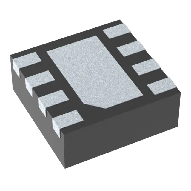
The TRF37A75 is packaged in a 2.00mm x 2.00mm
WSON with a power down pin feature making it ideal
for applications where space and low power modes
are critical.
2 Applications
•
•
•
•
•
•
•
•
•
•
•
•
•
•
•
•
•
•
•
General Purpose RF Gain Block
Consumer
Industrial
Utility Meters
Low-cost Radios
Cellular Base Station
Wireless Infrastructure
RF Backhaul
Radar
Electronic Warfare
Software-defined Radio
Test and Measurement
Point-to-Point/Multipoint Microwave
Software Defined Radios
RF Repeaters
Distributed Antenna Systems
LO and PA Driver Amplifier
Wireless Data, Satellite, DBS, CATV
IF Amplifier
The TRF37A75 is designed for ease of use. For
maximum flexibility, this family of parts uses a
common 5 V supply and consumes 80 mA. In
addition, this family was designed with an active bias
circuit that provides a stable and predictable bias
current over process, temperature and voltage
variations. For gain and linearity budgets the device
was designed to provide a flat gain response and
excellent OIP3 out to 6000 MHz. For space
constrained applications, this family is internally
matched to 50 Ω, which simplifies ease of use and
minimizes needed PCB area.
Device Information(1)
PART NUMBER
TRF37A75
PACKAGE
WSON (32)
BODY SIZE (NOM)
2.00mm x 2.00mm
(1) For all available packages, see the orderable addendum at
the end of the datasheet.
Simplified Schematic
VCC
R2
Rbias
1.8R
VCC
1
2
C1
1000pF
8
Output
Match
40 MHz – 6000 MHz
Gain Versions: 12 dB
Noise Figure: 4 dB
Output P1dB: 18 dBm at 2000 MHz
Output IP3: 32.5 dBm at 2000 MHz
Power Down Mode
Single Supply: 5 V
Stabilized Performance Over Temperature
Unconditionally Stable
Robust ESD: >1 kV HBM; >1 kV CDM
Input
Match
1
L1
RF choke
100nH
7
3
6
4
5
C2
1000pF
PWDN
1
An IMPORTANT NOTICE at the end of this data sheet addresses availability, warranty, changes, use in safety-critical applications,
intellectual property matters and other important disclaimers. PRODUCTION DATA.
�TRF37A75
SLOS871 – MAY 2014
www.ti.com
Table of Contents
1
2
3
4
5
6
7
Features ..................................................................
Applications ...........................................................
Description .............................................................
Revision History.....................................................
Pin Configuration and Functions .........................
Specifications.........................................................
1
1
1
2
3
4
6.1
6.2
6.3
6.4
6.5
6.6
6.7
4
4
4
4
5
5
6
Absolute Maximum Ratings ......................................
Handling Ratings.......................................................
Recommended Operating Conditions.......................
Thermal Information ..................................................
Electrical Characteristics...........................................
Timing Requirements ................................................
Typical Characteristics ..............................................
7.2 Functional Block Diagram ......................................... 8
7.3 Feature Description................................................... 8
7.4 Device Functional Modes.......................................... 8
8
Applications and Implementation ........................ 9
8.1 Application Information.............................................. 9
8.2 Typical Application ................................................... 9
9 Power Supply Recommendations...................... 10
10 Layout................................................................... 11
10.1 Layout Guidelines ................................................. 11
10.2 Layout Example .................................................... 11
11 Device and Documentation Support ................. 12
11.1 Trademarks ........................................................... 12
11.2 Electrostatic Discharge Caution ............................ 12
11.3 Glossary ................................................................ 12
Detailed Description .............................................. 8
12 Mechanical, Packaging, and Orderable
Information ........................................................... 12
7.1 Overview ................................................................... 8
4 Revision History
2
DATE
REVISION
NOTES
May 2014
*
Initial release.
Submit Documentation Feedback
Copyright © 2014, Texas Instruments Incorporated
Product Folder Links: TRF37A75
�TRF37A75
www.ti.com
SLOS871 – MAY 2014
5 Pin Configuration and Functions
DSG PACKAGE
(TOP VIEW)
8
NC
RFIN
2
7
RFOUT
NC
3
6
NC
NC
4
5
PWDN
Output
Match
1
Input
Match
VCC
Pin Functions
PIN
NAME
VCC
RFIN
NC
DESCRIPTION
NO.
1
DC Bias.
2
RF input. Connect to an RF source through a DC-blocking capacitor. Internally matched to 50 Ω.
3, 4, 6, 8
No electrical connection. Connect pad to GND for board level reliability integrity.
PWDN
5
When high the device is in power down state. When LOW or NC the device is in active state. Internal
pulldown resistor to GND.
RFOUT
7
RF Output and DC Bias (VCC). Connect to DC supply through an RF choke inductor. Connect to output
load through a DC-blocking capacitor. Internally matched to 50 Ω.
GND
PowerPAD™
RF and DC GND. Connect to PCB ground plane.
Submit Documentation Feedback
Copyright © 2014, Texas Instruments Incorporated
Product Folder Links: TRF37A75
3
�TRF37A75
SLOS871 – MAY 2014
www.ti.com
6 Specifications
6.1 Absolute Maximum Ratings
over operating free-air temperature range (unless otherwise noted)
(1)
Supply Input voltage
Input Power
MAX
UNIT
6
V
10
dBm
–40
150
°C
With recommended Rbias resistor
Operating virtual junction temperature range
(1)
MIN
–0.3
Stresses beyond those listed under Absolute Maximum Ratings may cause permanent damage to the device. These are stress ratings
only, which do not imply functional operation of the device at these or any other conditions beyond those indicated under Recommended
Operating Conditions. Exposure to absolute-maximum-rated conditions for extended periods may affect device reliability.
6.2 Handling Ratings
TSTG
VESD
(1)
(2)
MIN
MAX
UNIT
–65
150
°C
Human body model (HBM), per ANSI/ESDA/JEDEC
JS-001, all pins (1)
–1
1
kV
Charged device model (CDM), per JEDEC
specification JESD22-C101, all pins (2)
–1
1
kV
Storage temperature range
Electrostatic discharge
JEDEC document JEP155 states that 500-V HBM allows safe manufacturing with a standard ESD control process.
JEDEC document JEP157 states that 250-V CDM allows safe manufacturing with a standard ESD control process.
6.3 Recommended Operating Conditions
over operating free-air temperature range (unless otherwise noted)
MIN
NOM
MAX
UNIT
Supply Voltage, VCC
4.5
5
5.25
V
Operating junction temperature, TJ
–40
125
°C
6.4 Thermal Information
THERMAL METRIC (1)
DSG
8 PINS
RθJA
Junction-to-ambient thermal resistance
79.3
RθJCtop
Junction-to-case (top) thermal resistance
110
RθJB
Junction-to-board thermal resistance
49
ψJT
Junction-to-top characterization parameter
6
ψJB
Junction-to-board characterization parameter
49.4
RθJCbot
Junction-to-case (bottom) thermal resistance
19.2
(1)
4
UNIT
°C/W
For more information about traditional and new thermal metrics, see the IC Package Thermal Metrics application report, SPRA953.
Submit Documentation Feedback
Copyright © 2014, Texas Instruments Incorporated
Product Folder Links: TRF37A75
�TRF37A75
www.ti.com
SLOS871 – MAY 2014
6.5 Electrical Characteristics
VCC = 5 V, TA = 25°C, PWDN = Low, RBIAS = 1.8 Ω, LOUT = 100 nH, C1 = C2 = 1000 pF, ZS = ZL = 50 Ω (unless otherwise
noted)
PARAMETER
TEST CONDITIONS
MIN
TYP
MAX
80
95
UNIT
DC Parameters
ICC
Pdiss
Total supply current
Power down current
PWDN = High
Power dissipation
mA
125
µA
0.4
W
RF Frequency Range
Frequency range
G
Small signal gain
40
6000
MHz
fRF = 400 MHz
13
dB
fRF = 2000 MHz
12
dB
fRF = 3000 MHz
12
dB
fRF = 4000 MHz
12
dB
fRF = 5000 MHz
12
dB
fRF = 6000 MHz
11
dB
OP1dB
Output 1dB compression point
At 2000 MHz
19
dBm
OIP3
Output 3rd order intercept point
At 2000 MHz, 2-tone 10MHz apart
32.5
dBm
NF
Noise figure
At 2000 MHz
4
dB
R(LI)
Input return loss
At 2000 MHz
16
dB
R(LO)
Output return loss
At 2000 MHz
13
dB
PWDN Pin
VIH
High level input level
VIL
Low level input level
2
V
IIH
High level input current
30
µA
IIL
Low level input current
1
µA
0.8
V
6.6 Timing Requirements
MIN
TYP
MAX
UNIT
PWDN Pin
tON
Turn-on Time
50% TTL to 90% POUT
0.6
µs
tOFF
Turn-off Time
50% TTL to 10% POUT
1.4
µs
Submit Documentation Feedback
Copyright © 2014, Texas Instruments Incorporated
Product Folder Links: TRF37A75
5
�TRF37A75
SLOS871 – MAY 2014
www.ti.com
6.7 Typical Characteristics
0.00
±5.00
S[2,2]
S[1,1]
Sxx (dB)
±10.00
±15.00
±20.00
±25.00
±30.00
S11
S12
S21
±35.00
±40.00
0
1000
2000
3000
4000
5000
6000
Frequency (MHz)
C016
Freq [10.00 MHz to 6.000 GHz]
VCC = 5 V
Temp = 25°C
10 MHz to 6 GHz
Data Taken with EVM and Bias T, De-embedded to DUT pin
VCC = 5 V
Temp = 25°C
40 MHz to 6 GHz
Data Taken with EVM and Bias T, De-embedded to DUT pin
Figure 1. Smith Chart – S11, S22
Figure 2. S11, S12, S21
14
14.0
4.5 V
13.5
13
4.75 V
13.5
5V
13.0
±40C
25C
85C
12.5
Gain (dB)
Gain (dB)
5.25 V
12
11.5
12.5
12.0
11.5
11
11.0
10.5
10.5
10.0
10
0
1000
2000
3000
4000
5000
Frequency (MHz)
VCC curves
Temp = 25°C
0
6000
1000
Pin = –10 dBm
Temp curves
Figure 3. Gain vs Frequency
4000
5000
VCC = 5 V
6000
C002
Pin = –10 dBm
22
4.5
4.75
5
5.25
21
20
19
±40C
21
25C
20
OP1dB (dBm)
OP1dB (dBm)
3000
Figure 4. Gain vs Frequency
22
18
17
16
85C
19
18
17
16
15
15
14
14
13
13
12
12
0
1000
2000
3000
4000
5000
Frequency (MHz)
VCC curves
6000
0
1000
Temp = 25°C
2000
3000
4000
5000
Freuency (MHz)
C007
Temp curves
Figure 5. OP1dB vs Frequency
6
2000
Frequency (MHz)
C001
Submit Documentation Feedback
6000
C008
VCC = 5 V
Figure 6. OP1dB vs Frequency
Copyright © 2014, Texas Instruments Incorporated
Product Folder Links: TRF37A75
�TRF37A75
www.ti.com
SLOS871 – MAY 2014
35
35
33
33
31
31
29
29
OIP3 (dBm)
OIP3 (dBm)
Typical Characteristics (continued)
27
25
23
27
25
23
21
21
19
19
4.5
4.75
5
5.25
17
15
0
1000
2000
3000
4000
5000
VCC curves
Temp = 25°C
15
6000
Frequency (MHz)
-40
25
85
17
0
1000
Pin = –10 dBm/tone
Temp curves
3000
4000
5000
6000
VCC = 5 V
C005
Pin = –10 dBm/tone
Figure 8. OIP3 vs Frequency
6.0
6.0
5.5
5.5
5.0
5.0
4.5
4.5
NF (dB)
NF (dB)
Figure 7. OIP3 vs Frequency
4.0
3.5
-40
25
85
4.0
3.5
3.0
3.0
4.5
4.75
5
5.25
2.5
2.0
0
1000
2000
3000
4000
5000
VCC curves
2.5
2.0
6000
Frequency (MHz)
0
1000
Temp = 25°C
2000
3000
4000
5000
6000
Frequency (MHz)
C010
Temp curves
Figure 9. NF vs Frequency
C011
VCC = 5 V
Figure 10. NF vs Frequency
90
90
4.5
4.75
5
5.25
87
±40C
25C
87
84
ICC (mA)
ICC (mA)
2000
Frequency (MHz)
C004
81
78
85C
84
81
78
75
75
0
1000
2000
3000
4000
Frequency (MHz)
VCC curves
Temp = 25°C
5000
6000
0
1000
2000
3000
4000
5000
Frequency (MHz)
C013
Temp curves
Figure 11. ICC vs Frequency
6000
C014
VCC = 5 V
Figure 12. ICC vs Frequency
Submit Documentation Feedback
Copyright © 2014, Texas Instruments Incorporated
Product Folder Links: TRF37A75
7
�TRF37A75
SLOS871 – MAY 2014
www.ti.com
7 Detailed Description
7.1 Overview
The device is a 5 V general purpose RF gain block. It is a SiGe Darlington amplifier with integrated 50 Ω input
and output matching. The device contains an active bias circuit to maintain performance over a wide temperature
and voltage range. The included power down function allows the amplifier to shut down saving power when the
amplifier is not needed. Fast shut down and start up enable the amplifier to be used in a host of time division
duplex applications.
7.2 Functional Block Diagram
VCC
Output
Match
RF Input
Active Bias and
Temperature
Compensation
Input
Match
Power Down
VCC
RF Output
7.3 Feature Description
The TRF37A75 is a fixed gain RF amplifier. It is internally matched to 50 Ω on both the input and output. It is a
fully cascadable general purpose amplifier. The included active bias circuitry ensures the amplifier performance
is optimized over the full operating temperature and voltage ranges
7.4 Device Functional Modes
7.4.1 Power Down
The TRF37A75 PWDN pin can be left unconnected for normal operation or a logic-high for disable mode
operation. For applications that use the power down mode, normal 5 V TLL levels are supported.
8
Submit Documentation Feedback
Copyright © 2014, Texas Instruments Incorporated
Product Folder Links: TRF37A75
�TRF37A75
www.ti.com
SLOS871 – MAY 2014
8 Applications and Implementation
8.1 Application Information
The TRF37A75 is a wideband, high performance, general purpose RF amplifier. To maximize its performance,
good RF layout and grounding techniques should be employed.
8.2 Typical Application
The TRF37A75 device is typically placed in a system as illustrated in Figure 13.
VCC
C5
DC Bypass
Capacitor
DC Bias
R2 Resistor
C4
RF Bypass
Capacitors
C3
L1
RF In
1
VCC
2
RFIN
C1
3
DC Blocking
Capacitor
4
RF Choke
Inductor
8
RFOUT
PWDN
RF Out
7
6
C2
5
DC Blocking
Capacitor
Figure 13. Typical Application Schematic for TRF37A75
8.2.1 Design Requirements
Table 1. Design Parameters
PARAMETERS
EXAMPLE VALUES
Input power range
< 3 dBm
Output power
< 18 dBm
Operating frequency range
40 — 6000 MHz
8.2.2 Detailed Design Procedure
The TRF37A75 is a simple to use internally matched and cascadable RF amplifier. Following the recommended
RF layout with good quality RF components and local DC bypass capacitors will ensure optimal performance is
achieved. TI provides various support materials including S-Parameter and ADS models to allow the design to be
optimized to the user's particular performance needs.
Submit Documentation Feedback
Copyright © 2014, Texas Instruments Incorporated
Product Folder Links: TRF37A75
9
�TRF37A75
SLOS871 – MAY 2014
www.ti.com
22
22
20
20
18
18
16
16
14
14
12
12
OP1dB
10
10
NF
8
8
6
6
4
4
2
2
0
0
1000
NF (dB)
OP1dB (dBm)
8.2.3 Application Curve
2000
3000
4000
5000
0
6000
Frequency (MHz)
C017
Figure 14. OP1dB and NF vs Frequency
9 Power Supply Recommendations
All supplies may be generated from a common nominal 5 V source but should be isolated through decoupling
capacitors placed close to the device. The typical application schematic in Figure 13 is an excellent example.
Select capacitors with self-resonant frequency near the application frequency. When multiple capacitors are used
in parallel to create a broadband decoupling network, place the capacitor with the higher self-resonant frequency
closer to the device. Expensive tantalum capacitors are not needed for optimal performance.
10
Submit Documentation Feedback
Copyright © 2014, Texas Instruments Incorporated
Product Folder Links: TRF37A75
�TRF37A75
www.ti.com
SLOS871 – MAY 2014
10 Layout
10.1 Layout Guidelines
Good layout practice helps to enable excellent linearity and isolation performance. An example of good layout is
shown in Figure 15. In the example, only the top signal layer and its adjacent ground reference plane are shown.
• Excellent electrical connection from the PowerPAD™ to the board ground is essential. Use the recommended
footprint, solder the pad to the board, and do not include solder mask under the pad.
• Connect pad ground to device terminal ground on the top board layer.
• Verify that the return DC and RF current path have a low impedance ground plane directly under the package
and RF signal traces into and out of the amplifier.
• Ensure that ground planes on the top and any internal layers are well stitched with vias.
• Do not route RF signal lines over breaks in the reference ground plane.
• Avoid routing clocks and digital control lines near RF signal lines.
• Do not route RF or DC signal lines over noisy power planes. Ground is the best reference, although clean
power planes can serve where necessary.
• Place supply decoupling close to the device.
10.2 Layout Example
VCC
DC Bypass
Capacitor
Note: Single DC bypass capacitor
can be used as long as it is close to
the pin 1 and is tied to the common
ground plane
DC Bypass
Capacitor
RF Bypass
Capacitors
DC Bias
Resistor
RF Choke
Inductor
VCC 11
RF In
88
NC
RFIN
22
77 RFOUT
NC
33
66
NC
44
55 PWDN
DC Blocking
Capacitor
NC
RF Out
DC Blocking
Capacitor
Note: Ensure good RF microstrip or stripline traces are
used to connect the external components to the RF input
and output pins
Note: Ensure all components are connected to a common
RF/DC ground plane with plenty of vias
Figure 15. Layout
Submit Documentation Feedback
Copyright © 2014, Texas Instruments Incorporated
Product Folder Links: TRF37A75
11
�TRF37A75
SLOS871 – MAY 2014
www.ti.com
11 Device and Documentation Support
11.1 Trademarks
PowerPAD is a trademark of Texas Instruments.
11.2 Electrostatic Discharge Caution
These devices have limited built-in ESD protection. The leads should be shorted together or the device placed in conductive foam
during storage or handling to prevent electrostatic damage to the MOS gates.
11.3 Glossary
SLYZ022 — TI Glossary.
This glossary lists and explains terms, acronyms and definitions.
12 Mechanical, Packaging, and Orderable Information
The following pages include mechanical packaging and orderable information. This information is the most
current data available for the designated devices. This data is subject to change without notice and revision of
this document. For browser-based versions of this data sheet, refer to the left-hand navigation.
12
Submit Documentation Feedback
Copyright © 2014, Texas Instruments Incorporated
Product Folder Links: TRF37A75
�PACKAGE OPTION ADDENDUM
www.ti.com
11-Aug-2022
PACKAGING INFORMATION
Orderable Device
Status
(1)
Package Type Package Pins Package
Drawing
Qty
Eco Plan
(2)
Lead finish/
Ball material
MSL Peak Temp
Op Temp (°C)
Device Marking
(3)
Samples
(4/5)
(6)
TRF37A75IDSGR
ACTIVE
WSON
DSG
8
3000
RoHS & Green
NIPDAU
Level-1-260C-UNLIM
-40 to 85
A75I
Samples
TRF37A75IDSGT
ACTIVE
WSON
DSG
8
250
RoHS & Green
NIPDAU
Level-1-260C-UNLIM
-40 to 85
A75I
Samples
(1)
The marketing status values are defined as follows:
ACTIVE: Product device recommended for new designs.
LIFEBUY: TI has announced that the device will be discontinued, and a lifetime-buy period is in effect.
NRND: Not recommended for new designs. Device is in production to support existing customers, but TI does not recommend using this part in a new design.
PREVIEW: Device has been announced but is not in production. Samples may or may not be available.
OBSOLETE: TI has discontinued the production of the device.
(2)
RoHS: TI defines "RoHS" to mean semiconductor products that are compliant with the current EU RoHS requirements for all 10 RoHS substances, including the requirement that RoHS substance
do not exceed 0.1% by weight in homogeneous materials. Where designed to be soldered at high temperatures, "RoHS" products are suitable for use in specified lead-free processes. TI may
reference these types of products as "Pb-Free".
RoHS Exempt: TI defines "RoHS Exempt" to mean products that contain lead but are compliant with EU RoHS pursuant to a specific EU RoHS exemption.
Green: TI defines "Green" to mean the content of Chlorine (Cl) and Bromine (Br) based flame retardants meet JS709B low halogen requirements of


 工商网监
湘ICP备2023018690号
工商网监
湘ICP备2023018690号
