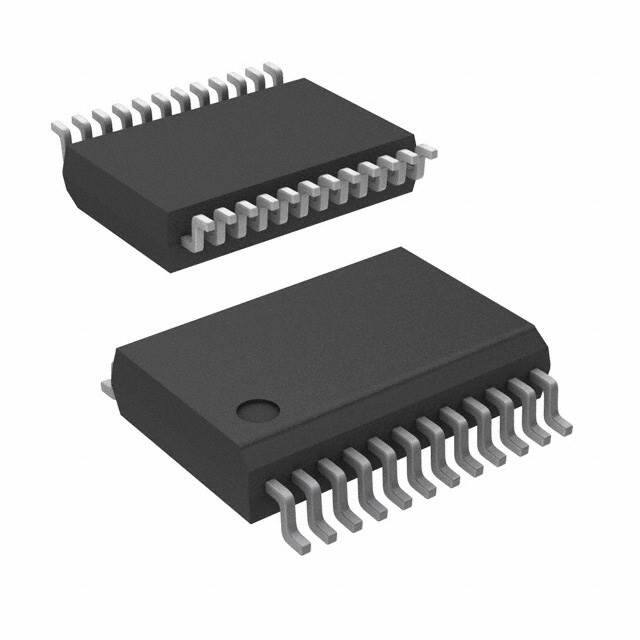
TRS207
5-V MULTICHANNEL RS-232 LINE DRIVER/RECEIVER
WITH ±15-kV ESD PROTECTION
www.ti.com
SLLS809 – JUNE 2007
FEATURES
•
•
•
•
•
•
ESD Protection for RS-232 Bus Pins
– ±15-kV Human-Body Model (HBM)
Meets or Exceeds the Requirements of
TIA/EIA-232-F and ITU v.28 Standards
Operates at 5-V VCC Supply
Operates up to 120 kbit/s
External Capacitors . . . 4 × 0.1 μF
Latch-Up Performance Exceeds 100 mA Per
JESD 78, Class II
DB OR DW PACKAGE
(TOP VIEW)
DOUT3
DOUT1
DOUT2
RIN1
ROUT1
DIN2
DIN1
GND
VCC
C1+
V+
C1−
APPLICATIONS
•
•
•
•
•
•
Battery-Powered Systems
PDAs
Notebooks
Laptops
Palmtop PCs
Hand-Held Equipment
1
24
2
23
3
22
4
21
5
20
6
19
7
18
8
17
9
16
10
15
11
14
12
13
DOUT4
RIN2
ROUT2
DIN5
DOUT5
DIN4
DIN3
ROUT3
RIN3
V−
C2−
C2+
DESCRIPTION/ORDERING INFORMATION
The TRS207 consists of five line drivers, three line receivers, and a dual charge-pump circuit with ±15-kV ESD
protection pin to pin (serial-port connection pins, including GND). The device meets the requirements of
TIA/EIA-232-F and provides the electrical interface between an asynchronous communication controller and the
serial-port connector. The charge pump and four small external capacitors allow operation from a single 5-V
supply. The devices operate at data signaling rates up to 120 kbit/s and a maximum of 30-V/μs driver output
slew rate.
ORDERING INFORMATION
PACKAGE (1) (2)
TA
0°C to 70°C
SOIC – DW
SSOP – DB
–40°C to 85°C
SOIC – DW
SSOP – DB
(1)
(2)
ORDERABLE PART NUMBER
Tube of 25
TRS207CDW
Reel of 2000
TRS207CDWR
Reel of 2000
TRS207CDBR
Tube of 25
TRS207IDW
Reel of 2000
TRS207IDWR
Reel of 2000
TRS207IDBR
TOP-SIDE MARKING
TRS207C
RU07C
TRS207I
RU07I
Package drawings, standard packing quantities, thermal data, symbolization, and PCB design guidelines are available at
www.ti.com/sc/package.
For the most current package and ordering information, see the Package Option Addendum at the end of this document, or see the TI
Web site at www.ti.com.
Please be aware that an important notice concerning availability, standard warranty, and use in critical applications of Texas
Instruments semiconductor products and disclaimers thereto appears at the end of this data sheet.
PRODUCTION DATA information is current as of publication date.
Products conform to specifications per the terms of the Texas
Instruments standard warranty. Production processing does not
necessarily include testing of all parameters.
Copyright © 2007, Texas Instruments Incorporated
�TRS207
5-V MULTICHANNEL RS-232 LINE DRIVER/RECEIVER
WITH ±15-kV ESD PROTECTION
www.ti.com
SLLS809 – JUNE 2007
FUNCTION TABLES
xxx
Each Driver (1)
(1)
INPUT
DIN
OUTPUT
DOUT
L
H
H
L
H = high level, L = low level
Each Receiver (1)
(1)
INPUT
RIN
OUTPUT
ROUT
L
H
H
L
Open
H
H = high level, L = low level,
Open = input disconnected or
connected driver off
LOGIC DIAGRAM (POSITIVE LOGIC)
7
2
DIN1
DOUT1
6
3
DIN2
TTL/CMOS
Inputs
DOUT2
18
1
DIN3
DOUT3
19
24
DIN4
DOUT4
21
20
DIN5
DOUT5
5
4
ROUT1
TTL/CMOS
Outputs
RIN1
22
23
ROUT2
RIN2
17
16
ROUT3
2
RS-232
Outputs
Submit Documentation Feedback
RIN3
RS-232
Inputs
�TRS207
5-V MULTICHANNEL RS-232 LINE DRIVER/RECEIVER
WITH ±15-kV ESD PROTECTION
www.ti.com
SLLS809 – JUNE 2007
Absolute Maximum Ratings
(1)
over operating free-air temperature range (unless otherwise noted)
VCC
Supply voltage range (2)
V+
Positive output supply voltage range (2)
V–
Negative output supply voltage range
VI
Input voltage range
VO
Output voltage range
(2)
Drivers
Receivers
V
VCC – 0.3
14
V
–14
0.3
V
–0.3
V+ + 0.3
V– – 0.3
V+ + 0.3
–0.3
VCC + 0.3
DOUT
Package thermal impedance (3) (4)
TJ
Operating virtual junction temperature
Tstg
Storage temperature range
(4)
6
UNIT
V
±30
Drivers
θJA
(2)
(3)
MAX
Receivers
Short-circuit duration
(1)
MIN
–0.3
V
Continuous
DB package
63
DW package
46
–65
°C/W
150
°C
150
°C
Stresses beyond those listed under "absolute maximum ratings" may cause permanent damage to the device. These are stress ratings
only, and functional operation of the device at these or any other conditions beyond those indicated under "recommended operating
conditions" is not implied. Exposure to absolute-maximum-rated conditions for extended periods may affect device reliability.
All voltages are with respect to network GND.
Maximum power dissipation is a function of TJ(max), θJA, and TA. The maximum allowable power dissipation at any allowable ambient
temperature is PD = (TJ(max) – TA)/θJA. Operating at the absolute maximum TJ of 150°C can affect reliability.
The package thermal impedance is calculated in accordance with JESD 51-7.
Recommended Operating Conditions (1)
See Figure 4
Supply voltage
VIH
Driver high-level input voltage
DIN
VIL
Driver low-level input voltage
DIN
Driver input voltage
DIN
VI
TA
(1)
NOM
MAX
4.5
5
5.5
2
TRS207C
TRS207I
UNIT
V
V
0.8
Receiver input voltage
Operating free-air temperature
MIN
0
5.5
–30
30
0
70
–40
85
V
V
°C
Test conditions are C1–C4 = 0.1 μF at VCC = 5 V ± 0.5 V.
Electrical Characteristics (1)
over recommended ranges of supply voltage (unless otherwise noted) (see Figure 4)
PARAMETER
ICC
(1)
Supply current
TEST CONDITIONS
No load,
VCC = 5 V,
MIN
TA = 25°C
TYP
MAX
11
20
UNIT
mA
Test conditions are C1–C4 = 0.1 μF at VCC = 5 V ± 0.5 V.
Submit Documentation Feedback
3
�TRS207
5-V MULTICHANNEL RS-232 LINE DRIVER/RECEIVER
WITH ±15-kV ESD PROTECTION
www.ti.com
SLLS809 – JUNE 2007
DRIVER SECTION
Electrical Characteristics (1)
over recommended ranges of supply voltage and operating free-air temperature (unless otherwise noted) (see Figure 4)
PARAMETER
TEST CONDITIONS
MIN
TYP (2)
VOH
High-level output voltage
DOUT at RL = 3 kΩ to GND,
DIN = GND
5
9
VOL
Low-level output voltage
DOUT at RL = 3 kΩ to GND,
DIN = VCC
–5
–9
IIH
High-level input current
VI = VCC
IIL
Low-level input current
VI at 0 V
IOS (3)
Short-circuit output current
VCC = 5.5 V,
VO = 0 V
ro
Output resistance
VCC, V+, and V– = 0 V,
VO = ±2 V
(1)
(2)
(3)
MAX
UNIT
V
V
μA
15
200
–15
–200
μA
±10
±60
mA
Ω
300
Test conditions are C1–C4 = 0.1 μF at VCC = 5 V ± 0.5 V.
All typical values are at VCC = 5 V, and TA = 25°C.
Short-circuit durations should be controlled to prevent exceeding the device absolute power dissipation ratings, and not more than one
output should be shorted at a time.
Switching Characteristics (1)
over recommended ranges of supply voltage and operating free-air temperature (unless otherwise noted) (see Figure 4)
PARAMETER
TEST CONDITIONS
MIN
TYP (2)
MAX
UNIT
Maximum data rate
CL = 50 pF to 1000 pF,
One DOUT switching,
RL = 3 kΩ to 7 kΩ,
See Figure 1
tPLH(D)
Propagation delay time,
low- to high-level output
CL = 2500 pF,
All drivers loaded,
RL = 3 kΩ,
See Figure 1
2
μs
tPHL(D)
Propagation delay time,
high- to low-level output
CL = 2500 pF,
All drivers loaded,
RL = 3 kΩ,
See Figure 1
2
μs
tsk(p)
Pulse skew (3)
CL = 150 pF to 2500 pF,
See Figure 2
RL = 3 kΩ to 7 kΩ,
300
ns
SR(tr)
Slew rate, transition region
(see Figure 1)
CL = 50 pF to 1000 pF,
VCC = 5 V
RL = 3 kΩ to 7 kΩ,
(1)
(2)
(3)
120
3
kbit/s
6
30
V/μs
Test conditions are C1–C4 = 0.1 μF at VCC = 5 V ± 0.5 V.
All typical values are at VCC = 5 V, and TA = 25°C.
Pulse skew is defined as |tPLH – tPHL| of each channel of the same device.
ESD Protection
PIN
DOUT, RIN
4
TEST CONDITIONS
Human-Body Model
Submit Documentation Feedback
TYP
UNIT
±15
kV
�TRS207
5-V MULTICHANNEL RS-232 LINE DRIVER/RECEIVER
WITH ±15-kV ESD PROTECTION
www.ti.com
SLLS809 – JUNE 2007
RECEIVER SECTION
Electrical Characteristics (1)
over recommended ranges of supply voltage and operating free-air temperature (unless otherwise noted) (see Figure 4)
PARAMETER
TEST CONDITIONS
VOH
High-level output voltage
IOH = –1 mA
VOL
Low-level output voltage
IOL = 1.6 mA
VIT+
Positive-going input threshold voltage
VCC = 5 V,
TA = 25°C
VIT–
Negative-going input threshold voltage
VCC = 5 V,
TA = 25°C
Vhys
Input hysteresis (VIT+ – VIT–)
ri
Input resistance
(1)
(2)
VI = ±3 V to ±25 V
MIN
TYP (2)
3.5
VCC – 0.4
1.7
MAX
UNIT
V
0.4
V
2.4
V
0.8
1.2
0.2
0.5
1
V
V
3
5
7
kΩ
Test conditions are C1–C4 = 0.1 μF at VCC = 5 V ± 0.5 V.
All typical values are at VCC = 5 V, and TA = 25°C.
Switching Characteristics (1)
over recommended ranges of supply voltage and operating free-air temperature (unless otherwise noted) (see Figure 3)
PARAMETER
TEST CONDITIONS
tPLH
Propagation delay time, low- to high-level output
tPHL
Propagation delay time, high- to low-level output
tsk(p)
(1)
(2)
(3)
Pulse skew
CL = 150 pF
(3)
MIN
TYP (2)
MAX
0.5
10
μs
0.5
10
μs
300
UNIT
ns
Test conditions are C1–C4 = 0.1 μF at VCC = 5 V ± 0.5 V.
All typical values are at VCC = 5 V, and TA = 25°C.
Pulse skew is defined as |tPLH – tPHL| of each channel of the same device.
Submit Documentation Feedback
5
�TRS207
5-V MULTICHANNEL RS-232 LINE DRIVER/RECEIVER
WITH ±15-kV ESD PROTECTION
www.ti.com
SLLS809 – JUNE 2007
PARAMETER MEASUREMENT INFORMATION
3V
Input
Generator
(see Note B)
1.5 V
RS-232
Output
50 Ω
RL
1.5 V
0V
tPHL (D)
CL
(see Note A)
Output
tPLH (D)
3V
3V
−3 V
−3 V
TEST CIRCUIT
SR(tr) +
t
PHL (D)
6V
or t
VOH
VOL
VOLTAGE WAVEFORMS
PLH (D)
A.
CL includes probe and jig capacitance.
B.
The pulse generator has the following characteristics: PRR = 120 kbit/s, ZO = 50 Ω, 50% duty cycle, tr ≤ 10 ns,
tf ≤ 10 ns.
Figure 1. Driver Slew Rate
3V
Generator
(see Note B)
RS-232
Output
50 Ω
RL
Input
1.5 V
1.5 V
0V
CL
(see Note A)
tPHL (D)
tPLH (D)
VOH
50%
50%
Output
VOL
TEST CIRCUIT
VOLTAGE WAVEFORMS
A.
CL includes probe and jig capacitance.
B.
The pulse generator has the following characteristics: PRR = 120 kbit/s, ZO = 50 Ω, 50% duty cycle, tr ≤ 10 ns,
tf ≤ 10 ns.
Figure 2. Driver Pulse Skew
Input
3V
1.5 V
1.5 V
−3 V
Output
Generator
(see Note B)
50 Ω
CL
(see Note A)
tPHL (R)
tPLH (R)
VOH
50%
Output
50%
VOL
TEST CIRCUIT
VOLTAGE WAVEFORMS
A.
CL includes probe and jig capacitance.
B.
The pulse generator has the following characteristics: ZO = 50 Ω, 50% duty cycle, tr ≤ 10 ns, tf ≤ 10 ns.
Figure 3. Receiver Propagation Delay Times
6
Submit Documentation Feedback
�TRS207
5-V MULTICHANNEL RS-232 LINE DRIVER/RECEIVER
WITH ±15-kV ESD PROTECTION
www.ti.com
SLLS809 – JUNE 2007
APPLICATION INFORMATION
DOUT3
DOUT1
1
24
2
23
DOUT4
RIN2
5 kΩ
3
DOUT2
22
4
RIN1
ROUT2
5V
5 kΩ
400 kΩ
21
5
ROUT1
20
5V
400 kΩ
19
5V
400 kΩ
DIN1
GND
400 kΩ
7
18
8
17
16
= 0.1µF
−
DIN4
5V
CBYPASS
+
DOUT5
5V
400 kΩ
6
DIN2
DIN5
DIN3
ROUT3
RIN3
C4 =
0.1 µF
16 V
5 kΩ
9
C3 † =
0.1 µF
6.3 V
V−
+
10
11
C1 =
0.1 µF
6.3 V
†
VCC
−
C1+
C2−
15
−
14
V+
−
+
+
−
12
C2+
C1−
+
13
C2 =
0.1 µF
16 V
C3 can be connected to VCC or GND.
A.
Resistor values shown are nominal.
B.
Nonpolarized ceramic capacitors are acceptable. If polarized tantalum or electrolytic capacitors are used, they should
be connected as shown.
Figure 4. Typical Operating Circuit and Capacitor Values
Submit Documentation Feedback
7
�TRS207
5-V MULTICHANNEL RS-232 LINE DRIVER/RECEIVER
WITH ±15-kV ESD PROTECTION
www.ti.com
SLLS809 – JUNE 2007
APPLICATION INFORMATION (continued)
Capacitor Selection
The capacitor type used for C1–C4 is not critical for proper operation. The TRS207 requires 0.1-μF capacitors,
although capacitors up to 10 μF can be used without harm. Ceramic dielectrics are suggested for the 0.1-μF
capacitors. When using the minimum recommended capacitor values, make sure the capacitance value does
not degrade excessively as the operating temperature varies. If in doubt, use capacitors with a larger (e.g., 2×)
nominal value. The capacitors' effective series resistance (ESR), which usually rises at low temperatures,
influences the amount of ripple on V+ and V–.
Use larger capacitors (up to 10 μF) to reduce the output impedance at V+ and V–.
Bypass VCC to ground with at least 0.1 μF. In applications sensitive to power-supply noise generated by the
charge pumps, decouple VCC to ground with a capacitor the same size as (or larger than) the charge-pump
capacitors (C1–C4).
Electrostatic Discharge (ESD) Protection
TI TRS207 devices have standard ESD protection structures incorporated on the pins to protect against
electrostatic discharges encountered during assembly and handling. In addition, the RS-232 bus pins (driver
outputs and receiver inputs) of these devices have an extra level of ESD protection. Advanced ESD structures
were designed to successfully protect these bus pins against ESD discharge of ±15-kV when powered down.
ESD Test Conditions
ESD testing is stringently performed by TI, based on various conditions and procedures. Please contact TI for a
reliability report that documents test setup, methodology, and results.
Human-Body Model (HBM)
The HBM of ESD testing is shown in Figure 5, while Figure 6 shows the current waveform that is generated
during a discharge into a low impedance. The model consists of a 100-pF capacitor, charged to the ESD voltage
of concern, and subsequently discharged into the DUT through a 1.5-kΩ resistor.
RD
1.5 kΩ
VHBM
+
−
CS
100 pF
Figure 5. HBM ESD Test Circuit
8
Submit Documentation Feedback
DUT
�TRS207
5-V MULTICHANNEL RS-232 LINE DRIVER/RECEIVER
WITH ±15-kV ESD PROTECTION
www.ti.com
SLLS809 – JUNE 2007
APPLICATION INFORMATION (continued)
1.5
VHBM = 2 kV
I DUT (A)
1.0
0.5
DUT = 10-V 1-Ω Zener Diode
0.0
0
50
100
150
200
Time (ns)
Figure 6. Typical HBM Current Waveform
Machine Model (MM)
The MM ESD test applies to all pins using a 200-pF capacitor with no discharge resistance. The purpose of the
MM test is to simulate possible ESD conditions that can occur during the handling and assembly processes of
manufacturing. In this case, ESD protection is required for all pins, not just RS-232 pins. However, after PC
board assembly, the MM test is no longer as pertinent to the RS-232 pins.
Submit Documentation Feedback
9
�PACKAGE OPTION ADDENDUM
www.ti.com
29-Mar-2023
PACKAGING INFORMATION
Orderable Device
Status
(1)
Package Type Package Pins Package
Drawing
Qty
Eco Plan
(2)
Lead finish/
Ball material
MSL Peak Temp
Op Temp (°C)
Device Marking
(3)
(4/5)
(6)
TRS207CDBR
NRND
SSOP
DB
24
2000
RoHS & Green
NIPDAU
Level-1-260C-UNLIM
0 to 70
RU07C
(1)
The marketing status values are defined as follows:
ACTIVE: Product device recommended for new designs.
LIFEBUY: TI has announced that the device will be discontinued, and a lifetime-buy period is in effect.
NRND: Not recommended for new designs. Device is in production to support existing customers, but TI does not recommend using this part in a new design.
PREVIEW: Device has been announced but is not in production. Samples may or may not be available.
OBSOLETE: TI has discontinued the production of the device.
(2)
RoHS: TI defines "RoHS" to mean semiconductor products that are compliant with the current EU RoHS requirements for all 10 RoHS substances, including the requirement that RoHS substance
do not exceed 0.1% by weight in homogeneous materials. Where designed to be soldered at high temperatures, "RoHS" products are suitable for use in specified lead-free processes. TI may
reference these types of products as "Pb-Free".
RoHS Exempt: TI defines "RoHS Exempt" to mean products that contain lead but are compliant with EU RoHS pursuant to a specific EU RoHS exemption.
Green: TI defines "Green" to mean the content of Chlorine (Cl) and Bromine (Br) based flame retardants meet JS709B low halogen requirements of