TS3A24159
SCDS238H – MARCH 2007 – REVISED AUGUST 2022
TS3A24159 0.3-Ω 2-Channel SPDT Bidirectional Analog Switch
Dual-Channel 2:1 Multiplexer and Demultiplexer
1 Features
3 Description
•
•
•
•
•
•
•
•
The TS3A24159 is a 2-channel single-pole doublethrow (SPDT) bidirectional analog switch that is
designed to operate from 1.65 V to 3.6 V. It
offers low ON-state resistance and excellent ONstate resistance matching with the break-beforemake feature, to prevent signal distortion during the
transferring of a signal from one channel to another.
The device has excellent total harmonic distortion
(THD) performance, low ON-state resistence, and
consumes very low power. These are some of the
features that make this device suitable for a variety of
markets and many different applications.
•
Specified break-before-make switching
Low ON-state resistance (0.3 Ω maximum)
Low charge injection
Excellent ON-state resistance matching
Low total harmonic distortion (THD)
1.65-V to 3.6-V single-supply operation
Control inputs are 1.8-V logic compatible
Latch-up performance exceeds 100 mA per JESD
78, Class II
ESD performance tested per JESD 22
– 2000-V Human-Body Model
(A114-B, Class II)
– 1000-V Charged-Device Model (C101)
Device Information(1)
2 Applications
•
•
•
•
•
•
•
•
•
•
PART NUMBER
Cell phones
Personal digital assistant (PDAs)
Portable instrumentation
Audio and video signal routing
Low-voltage data-acquisition systems
Communication circuits
Modems
Hard drives
Computer peripherals
Wireless terminals and peripherals
TS3A24159
(1)
PACKAGE
BODY SIZE (NOM)
VSSOP (10)
3.00 mm × 3.00 mm
VSON (10)
3.00 mm × 3.00 mm
DSBGA (10)
1.86 mm × 1.35 mm
For all available packages, see the orderable addendum at
the end of the data sheet.
SPDT
NC1
COM1
NO1
IN1
Logic
Control
SPDT
NC2
COM2
NO2
IN2
Logic
Control
Functional Block Diagram
An IMPORTANT NOTICE at the end of this data sheet addresses availability, warranty, changes, use in safety-critical applications,
intellectual property matters and other important disclaimers. PRODUCTION DATA.
�TS3A24159
www.ti.com
SCDS238H – MARCH 2007 – REVISED AUGUST 2022
Table of Contents
1 Features............................................................................1
2 Applications..................................................................... 1
3 Description.......................................................................1
4 Revision History.............................................................. 2
5 Pin Configuration and Functions...................................3
6 Specifications.................................................................. 5
6.1 Absolute Maximum Ratings........................................ 5
6.2 ESD Ratings............................................................... 5
6.3 Recommended Operating Conditions.........................5
6.4 Thermal Information....................................................6
6.5 Electrical Characteristics for 3-V Supply.....................6
6.6 Electrical Characteristics for 2.5-V Supply..................7
6.7 Electrical Characteristics for 1.8-V Supply..................9
6.8 Switching Characteristics for a 3-V Supply............... 10
6.9 Switching Characteristics for a 2.5-V Supply............ 10
6.10 Switching Characteristics for a 1.8-V Supply.......... 11
6.11 Typical Characteristics............................................ 12
7 Parameter Measurement Information.......................... 14
8 Detailed Description......................................................18
8.1 Overview................................................................... 18
8.2 Functional Block Diagram......................................... 18
8.3 Feature Description...................................................18
8.4 Device Functional Modes..........................................18
9 Application and Implementation.................................. 19
9.1 Application Information............................................. 19
9.2 Typical Application.................................................... 19
10 Power Supply Recommendations..............................20
11 Layout........................................................................... 21
11.1 Layout Guidelines................................................... 21
11.2 Layout Example...................................................... 21
12 Device and Documentation Support..........................22
12.1 Documentation Support.......................................... 22
12.2 Receiving Notification of Documentation Updates..22
12.3 Support Resources................................................. 22
12.4 Trademarks............................................................. 22
12.5 Electrostatic Discharge Caution..............................22
12.6 Glossary..................................................................22
13 Mechanical, Packaging, and Orderable
Information.................................................................... 22
4 Revision History
NOTE: Page numbers for previous revisions may differ from page numbers in the current version.
Changes from Revision G (February 2022) to Revision H (August 2022)
Page
• Changed the maximum VCC from: 3.6 V to: 4 V ................................................................................................ 5
Changes from Revision F (September 2019) to Revision G (February 2022)
Page
• Updated the numbering format for tables, figures, and cross-references throughout the document..................1
• Updated the part number in the Detailed Design Procedure ........................................................................... 20
Changes from Revision E (March 2019) to Revision F (September 2019)
Page
• Changed the YZP package image view From: Top-Through View To: Bottom View.......................................... 3
Changes from Revision D (July 2015) to Revision E (March 2019)
Page
• Changed the YZP package image and deleted the YZP Package, Terminal Assignments table....................... 3
• Changed Turnon time VCC (Full) value From: 2.3 V to 2.7 V To: 2.7 V to 3.6 V in Switching Characteristics for
a 3-V Supply .................................................................................................................................................... 10
• Changed Turnon time VCC (Full) value From: 2.3 V to 2.7 V To: 2.7 V to 3.6 V in Switching Characteristics for
a 2.5-V Supply ................................................................................................................................................. 10
Changes from Revision C (February 2008) to Revision D (March 2015)
Page
• Added Pin Configuration and Functions section, ESD Ratings table, Feature Description section, Device
Functional Modes, Application and Implementation section, Power Supply Recommendations section, Layout
section, Device and Documentation Support section, and Mechanical, Packaging, and Orderable Information
section ............................................................................................................................................................... 1
• Changed V+ to VCC throughout the document to meet JEDEC standards.........................................................1
2
Submit Document Feedback
Copyright © 2022 Texas Instruments Incorporated
Product Folder Links: TS3A24159
�TS3A24159
www.ti.com
SCDS238H – MARCH 2007 – REVISED AUGUST 2022
5 Pin Configuration and Functions
VCC
VCC
10 NO2
1
1
10 NO2
NO1 2
9
COM2
8
IN2
NC2
COM1 3
IN1 4
7
NC2
GND
NC1 5
6
GND
NO1 2
9
COM2
COM1 3
8
IN2
IN1 4
7
NC1 5
6
Figure 5-1. DGS Package, 10-Pin VSSOP (Top
View)
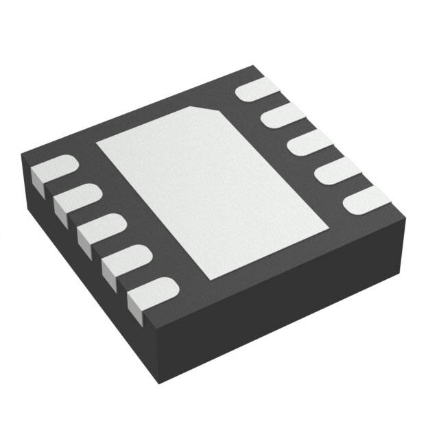
Figure 5-2. DRC Package, 10-Pin VSON (Top View)
Table 5-1. Pin Functions – VSSOP and VSON
PIN
NO.
1
NAME
TYPE(1)
DESCRIPTION
VCC
—
Power supply
2
NO1
I/O
Normally open signal path
3
COM1
I/O
Common signal path
4
IN1
I
5
NC1
I/O
Digital control to connect COM to NO or NC
Normally closed signal path
6
GND
—
Ground
7
NC2
I/O
Normally closed signal path
8
IN2
I
9
COM2
I/O
Digital control to connect COM to NO or NC
Common signal path
10
NO2
I/O
Normally open signal path
(1)
I = input, O = output
Submit Document Feedback
Copyright © 2022 Texas Instruments Incorporated
Product Folder Links: TS3A24159
3
�TS3A24159
www.ti.com
SCDS238H – MARCH 2007 – REVISED AUGUST 2022
1
2
V
3
D
NO1
C
COM1
COM2
B
IN1
IN2
A
NC1
CC
GND
NO2
NC2
Not to scale
Figure 5-3. YZP Package, 10-Pin DSBGA (Bottom View)
Legend
Input or Output
Input
Ground
Power
Table 5-2. Pin Functions – DSBGA
PIN
NO.
NAME
A1
NC1
A2
A3
DESCRIPTION
I/O
Normally closed signal path
GND
—
Ground
NC2
I/O
Normally closed signal path
B1
IN1
I
Digital control to connect COM to NO or NC
B3
IN2
I
Digital control to connect COM to NO or NC
C1
COM1
I/O
Common signal path
C3
COM2
I/O
Common signal path
D1
NO1
I/O
Normally open signal path
D2
VCC
—
Power supply
D3
NO2
I/O
Normally open signal path
(1)
4
TYPE(1)
I = input, O = output
Submit Document Feedback
Copyright © 2022 Texas Instruments Incorporated
Product Folder Links: TS3A24159
�TS3A24159
www.ti.com
SCDS238H – MARCH 2007 – REVISED AUGUST 2022
6 Specifications
6.1 Absolute Maximum Ratings
over operating free-air temperature range (unless otherwise noted) (1) (2)
MIN
MAX
VCC
Supply voltage(3)
–0.5
4
V
VNC
VNO
VCOM
Signal voltage(3) (4)
–0.5
VCC + 0.5
V
II/OK
Analog port diode current
–50
50
INC
INO
ICOM
ON-state switch current
–300
300
–500
500
VIN
Digital input voltage
–0.5
3.6
ON-state peak switch
VNC, VNO, VCOM < 0
current(3)
IIK
Digital input clamp
ICC
Continuous current through VCC
IGND
Continuous current through GND
Tstg
Storage temperature
(1)
(2)
(3)
(4)
(5)
VNC, VNO, VCOM = 0 to VCC
current(5)
VI < 0
UNIT
mA
mA
V
–50
mA
100
mA
–100
mA
–65
150
°C
Stresses beyond those listed under Absolute Maximum Ratings may cause permanent damage to the device. These are stress
ratings only, which do not imply functional operation of the device at these or any other conditions beyond those indicated under
Recommended Operating Conditions. Exposure to absolute-maximum-rated conditions for extended periods may affect device
reliability.
The algebraic convention, whereby the most negative value is a minimum and the most positive value is a maximum.
All voltages are with respect to ground, unless otherwise specified.
This value is limited to 5.5 V maximum.
Pulse at 1-ms duration
很抱歉,暂时无法提供与“TS3A24159DRCR”相匹配的价格&库存,您可以联系我们找货
免费人工找货- 国内价格 香港价格
- 1+8.640131+1.11659
- 10+6.1835610+0.79912
- 25+5.5753425+0.72052
- 100+4.90738100+0.63420
- 250+4.58892250+0.59304
- 500+4.39661500+0.56819
- 1000+4.265011000+0.55118
- 国内价格
- 1+5.65920
- 10+4.55760
- 30+3.99600
- 100+3.44520
- 500+3.12120
- 1000+2.94840