TS3DV421
www.ti.com
SCDS264D – JANUARY 2008 – REVISED JANUARY 2010
4-CHANNEL DIFFERENTIAL 8:16 MULTIPLEXER SWITCH FOR DVI/HDMI APPLICATIONS
Check for Samples: TS3DV421
FEATURES
1
•
•
•
•
•
APPLICATIONS
•
•
DVI/HDMI Signal Switching
Differential DVI, HDMI Signal Multiplexing for
Audio/Video Receivers and High-Definition
Televisions (HDTVs)
VSS
VDD
VSS
40
39
VDD
42
41
38
ATMDS2+
2
37
ATMDS2–
TMDS2+
3
36
ATMDS1+
TMDS2–
4
35
ATMDS1–
VSS
5
34
ATMDS0+
TMDS1+
6
33
ATMDS0–
TMDS1–
VDD
7
32
ATMDSCLK+
31
ATMDSCLK–
SEL
VSS
9
30
VDD
10
29
BTMDS2+
TMDS0+
11
28
BTMDS2–
TMDS0–
12
27
BTMDS1+
VSS
13
26
BTMDS1–
TMDSCLK+
14
25
BTMDS0+
TMDSCLK–
VDD
15
24
BTMDS0–
16
23
BTMDSCLK+
VSS
17
22
BTMDSCLK–
8
20
21
VSS
Exposed
Center
Pad
VDD
•
1
19
•
VSS
VDD
18
•
•
•
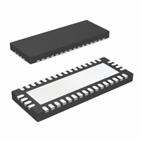
RUA PACKAGE
(TOP VIEW)
VSS
•
Compatible With HDMI v1.3 DVI 1.0
High-Speed Digital Interface
– Wide Bandwidth of Over 3.8 Gbps
– Serial Data Stream at 10× Pixel Clock Rate
– Supports All Video Formats up to 1080p
and SXGA (1280 × 1024 at 75 Hz)
– High Bandwidth of 4.95 Gbps (Single Link)
– HDCP Compatible
Low Crosstalk
(XTALK = –50 dB Typ at 1.65 Gbps)
Off Isolation (OIRR = –50 dB Typ at 1.65 Gbps)
Low Bit-to-Bit Skew (tsk(o) = 0.1 ns Max)
Low and Flat ON-State Resistance
(rON = 12.5 Ω Max, rON(flat) = 0.5 Ω Typ)
Low Input/Output Capacitance
(CON = 4.5 pF Max)
Enables Application-Specific Operating
Voltage Selection
– VDD Operating Range From 1.5 V to 2.1 V
When VSS = GND
– VDD Operating Range From 3.0 V to 3.6 V
When VSS = 1.5 V
Ioff Supports Partial-Power-Down Mode
Operation
Latch-Up Performance Exceeds 100 mA Per
JESD 78, Class II
ESD Performance Tested Per JESD 22
– 2000-V Human-Body Model
(A114-B, Class II)
– 1000-V Charged-Device Model (C101)
For DisplayPort Applications:
VDD = 1.8 V , VSS = GND
For HDMI /DVI Applications:
VDD = 3.3 V , VSS = 1.5 V
VDD
•
2
For RUA, the exposed center pad must be
connected to VSS or electronically open.
For this part to be used in HDMI/TMDS
applications, VSS can be elevated to 1.5 V.
See Figure 1.
DGV PACKAGE
(TOP VIEW)
VSS
VDD
VSS
VDD
VSS
TMDS2+
TMDS2–
VSS
TMDS1+
TMDS1–
VSS
VDD
SEL
VSS
TMDS0+
TMDS0–
VSS
TMDSCLK+
TMDSCLK–
VSS
VDD
VSS
VDD
VSS
1
48
2
47
3
46
4
45
5
44
6
43
7
42
8
41
9
40
10
39
11
38
12
37
13
36
14
35
15
34
16
33
17
32
18
31
19
30
20
29
21
28
22
27
23
26
24
25
VDD
VSS
ATMDS2+
ATMDS2–
ATMDS1+
ATMDS1–
VSS
ATMDS0+
ATMDS0–
ATMDSCLK+
ATMDSCLK–
VSS
VDD
BTMDS2+
BTMDS2–
BTMDS1+
BTMDS1–
VSS
BTMDS0+
BTMDS0–
BTMDSCLK+
BTMDSCLK–
VSS
VDD
1
2
Please be aware that an important notice concerning availability, standard warranty, and use in critical applications of Texas
Instruments semiconductor products and disclaimers thereto appears at the end of this data sheet.
All trademarks are the property of their respective owners.
PRODUCTION DATA information is current as of publication date.
Products conform to specifications per the terms of the Texas
Instruments standard warranty. Production processing does not
necessarily include testing of all parameters.
Copyright © 2008–2010, Texas Instruments Incorporated
�TS3DV421
SCDS264D – JANUARY 2008 – REVISED JANUARY 2010
www.ti.com
DESCRIPTION/ORDERING INFORMATION
The TS3DV421 is a 4-channel differential 2:1 multiplexer/demultiplexer digital video switch controlled with one
select input (SEL). SEL controls the data path of the multiplexer/demultiplexer and can be connected to any
GPIO in the system, using an external voltage divider system. The device provides high bandwidth necessary for
DVI and HDMI applications. This device expands the high-speed physical link interface from a single HDMI port
to two HDMI ports (A or B port). The unselected channel is set to a high-impedance state.
The most common application for the TS3DV421 is in the sink application. In this case, there are two sources
(i.e., DVD, set-top box, or game console) that must be routed to one HDMI receiver. The TS3DV421 can route
the signals where one HDMI receiver (in a DLP, LCD TV, PDP, or other high-definition display) can be expanded
to three ports.
The HDMI application calls for a 100-Ω differential impedance between the differential lines (TMDSn+ and
TMDSn–). Additionally, because the TS3DV421 is a high-bandwidth, low-rON pass transistor-type switch, a
properly designed board retains a 100-Ω differential impedance through the switch. The unselected port is in the
high-impedance mode, such that the receiver receives information from only one source. HDCP encryption is
passed through the switch for the HDMI receiver to decode.
Table 1. ORDERING INFORMATION
PACKAGE (1)
TA
–40°C to 85°C
(1)
(2)
(2)
ORDERABLE PART NUMBER
TOP-SIDE MARKING
QFN – RUA
Tape and reel
TS3DV421RUAR
SD421
TVSOP – DGV
Tape and reel
TS3DV421DGVR
SD421
Package drawings, thermal data, and symbolization are available at www.ti.com/packaging.
For the most current package and ordering information, see the Package Option Addendum at the end of this document, or see the TI
website at www.ti.com.
TYPICAL APPLICATION
DDC/CEC/+5V
HDMI
Transmitter 1
ATMDS0+
ATMDS0–
ATMDS1+
ATMDS1–
ATMDS2+
ATMDS2–
ATMDSCLK+
ATMDSCLK–
ATMDS0+
ATMDS0–
ATMDS1+
ATMDS1–
ATMDS2+
ATMDS2–
ATMDSCLK+
ATMDSCLK–
TS3DV421
HDMI Switch
HDMI
Transmitter 2
BTMDS0+
BTMDS0–
BTMDS1+
BTMDS1–
BTMDS2+
BTMDS2–
BTMDSCLK+
BTMDSCLK–
BTMDS0+
BTMDS0–
BTMDS1+
BTMDS1–
BTMDS2+
BTMDS2–
BTMDSCLK+
BTMDSCLK–
TMDS0+
TMDS0–
TMDS1+
TMDS1–
TMDS2+
TMDS2–
TMDSCLK+
TMDSCLK–
HDMI
Receiver
HDMI Scalar/
Video Decoder
Display
(DLP, LCD, TV,
PDP, HDTV)
DDC/CEC/+5V
2
Submit Documentation Feedback
Copyright © 2008–2010, Texas Instruments Incorporated
Product Folder Link(s): TS3DV421
�TS3DV421
www.ti.com
SCDS264D – JANUARY 2008 – REVISED JANUARY 2010
Table 2. FUNCTION TABLE
SEL
FUNCTION
OUTPUT
L
TMDSn+ = ATMDSn+
TMDSn– = ATMDSn–
TMDSCLK+ = ATMDSCLK+
TMDSCLK– = ATMDSCLK–
BTMDSn+ = High impedance
BTMDSn– = High impedance
BTMDSCLK+ = High impedance
BTMDSCLK– = High impedance
TMDSn+
TMDSn–
TMDSCLK+
TMDSCLK–
H
TMDSn+ = BTMDSn+
TMDSn– = BTMDSn–
TMDSCLK+ = BTMDSCLK+
TMDSCLK– = BTMDSCLK–
ATMDSn+ = High impedance
ATMDSn– = High impedance
ATMDSCLK+ = High impedance
ATMDSCLK– = High impedance
TMDSn+
TMDSn–
TMDSCLK+
TMDSCLK–
FUNCTIONAL DIAGRAM
TMDS2+
3 (6)
38 (46)
4 (7)
37 (45)
TMDS2–
29 (35)
28 (34)
TMDS1+
TMDS1–
6 (9)
36 (44)
7 (10)
35 (43)
27 (33)
26 (32)
TMDS0+
TMDS0–
11 (15)
34 (41)
12 (16)
33 (40)
25 (30)
24 (29)
TMDSCLK+
TMDSCLK–
14 (18)
32 (39)
15 (19)
31 (38)
23 (28)
22 (27)
SEL
A.
ATMDS2+
ATMDS2–
BTMDS2+
BTMDS2–
ATMDS1+
ATMDS1–
BTMDS1+
BTMDS1–
ATMDS0+
ATMDS0–
BTMDS0+
BTMDS0–
ATMDSCLK+
ATMDSCLK–
BTMDSCLK+
BTMDSCLK–
9 (13)
Control Logic
TVSOP package pin identification in parenthesis.
Submit Documentation Feedback
Copyright © 2008–2010, Texas Instruments Incorporated
Product Folder Link(s): TS3DV421
3
�TS3DV421
SCDS264D – JANUARY 2008 – REVISED JANUARY 2010
www.ti.com
TERMINAL FUNCTIONS
TERMINAL
NAME
4
NO.
TYPE
QFN (RUA)
TVSOP (DGV)
DESCRIPTION
ATMDS0–
33
40
I/O
Port A, channel 0, TMDS negative signal
ATMDS0+
34
41
I/O
Port A, channel 0, TMDS positive signal
ATMDS1–
35
43
I/O
Port A, channel 1, TMDS negative signal
ATMDS1+
36
44
I/O
Port A, channel 1, TMDS positive signal
ATMDS2–
37
45
I/O
Port A, channel 2, TMDS negative signal
ATMDS2+
38
46
I/O
Port A, channel 2, TMDS positive signal
ATMDSCLK–
31
38
I/O
Port A TMDS negative clock
ATMDSCLK+
32
39
I/O
Port A TMDS positive clock
BTMDS0–
24
29
I/O
Port B, channel 0, TMDS negative signal
BTMDS0+
25
30
I/O
Port B, channel 0, TMDS positive signal
BTMDS1–
26
32
I/O
Port B, channel 1, TMDS negative signal
BTMDS1+
27
33
I/O
Port B, channel 1, TMDS positive signal
BTMDS2–
28
34
I/O
Port B, channel 2, TMDS negative signal
BTMDS2+
29
35
I/O
Port B, channel 2, TMDS positive signal
BTMDSCLK–
22
27
I/O
Port B TMDS negative clock
BTMDSCLK+
23
28
I/O
Port B TMDS positive clock
SEL
9
13
I
Select pin to choose between port A or port B. Referenced to VSS
TMDS0–
12
16
I/O
TMDS channel 0 negative signal
TMDS0+
11
15
I/O
TMDS channel 0 positive signal
TMDS1–
7
10
I/O
TMDS channel 1 negative signal
TMDS1+
6
9
I/O
TMDS channel 1 positive signal
TMDS2–
4
7
I/O
TMDS channel 2 negative signal
TMDS2+
3
6
I/O
TMDS channel 2 positive signal
TMDSCLK–
15
19
I/O
TMDS negative clock
TMDS positive clock
TMDSCLK+
14
18
I/O
VDD
2, 8, 16,
18, 20, 30,
40, 42
2, 4, 12,
21, 23, 25,
36, 48
Power
Positive power supply voltage
VSS
1, 5, 10,
13, 17, 19,
21, 39, 41
1, 3, 5,
8, 14, 17,
20, 22, 24,
26, 31, 37,
42, 47
Power
Negative power supply voltage
Submit Documentation Feedback
Copyright © 2008–2010, Texas Instruments Incorporated
Product Folder Link(s): TS3DV421
�TS3DV421
www.ti.com
SCDS264D – JANUARY 2008 – REVISED JANUARY 2010
ABSOLUTE MINIMUM AND MAXIMUM RATINGS (1)
over operating free-air temperature range (unless otherwise noted), - All voltages are with respect to VSS
MIN
MAX
VDD
Supply voltage range
–0.5
2.5
V
VIN
Control input voltage range (2)
–0.5
2.5
V
VI/O
Switch I/O voltage range (2)
–0.5
2.5
V
IIK
Control input clamp current
VIN < VSS
50
mA
II/OK
I/O port clamp current
VI/O < VSS
50
mA
II/O
ON-state switch current (4)
100
mA
IDD
Continuous current through VDD
100
mA
ISS
Continuous current through VSS
100
mA
(3)
θJA
Package thermal impedance (5)
Tstg
Storage temperature range
(1)
(2)
(3)
(4)
(5)
DGV package
58.0
RUA package
51.2
–65
150
UNIT
°C/W
°C
Stresses beyond those listed under "absolute maximum ratings" may cause permanent damage to the device. These are stress ratings
only, and functional operation of the device at these or any other conditions beyond those indicated under "recommended operating
conditions" is not implied. Exposure to absolute-maximum-rated conditions for extended periods may affect device reliability.
The input and output voltage ratings may be exceeded if the input and output clamp-current ratings are observed.
VI and VO are used to denote specific conditions for VI/O.
II and IO are used to denote specific conditions for II/O.
The package thermal impedance is calculated in accordance with JESD 51-7.
RECOMMENDED OPERATING CONDITIONS
over operating free-air temperature range (unless otherwise noted)
MIN
TYP
MAX
VSS = GND
1.5
1.8
2.1
VSS = 1.5 V
3
3.3
3.6
UNIT
VDD
Supply voltage
VIH
High-level input voltage
3 V < VDD < 3.6 V, VSS = 1.5 V
VIL
Low-level input voltage
1.5 V < VDD < 2.1 V, VSS = 0 V
VIO
Switch input/output voltage
0
VDD
V
TA
Operating free-air temperature
0
85
°C
0.65(VDD – VSS)
+ VSS
V
0.35(VDD – VSS)
+ VSS
Submit Documentation Feedback
Copyright © 2008–2010, Texas Instruments Incorporated
Product Folder Link(s): TS3DV421
V
V
5
�TS3DV421
SCDS264D – JANUARY 2008 – REVISED JANUARY 2010
www.ti.com
ELECTRICAL CHARACTERISTICS FOR 1.8-V SUPPLY (1)
VDD = 1.5 V to 2.1 V, VSS = 0 V, TA = –40°C to 85°C (unless otherwise noted)
PARAMETER
TEST CONDITIONS
MIN
TYP (2)
MAX
–0.7
–1.2
V
UNIT
VIK
SEL
VDD = 2.1 V,
IIN = –18 mA
IIH
SEL
VDD = 2.1 V,
VIN = VDD
±1
μA
IIL
SEL
VDD = 2.1 V,
VIN = VSS
±1
μA
Ioff
VDD = 0,
VO = 0 to 2.1 V,
VI = 0
ICC
VDD = 2.1 V,
II/O = 0,
Switch ON or OFF
CIN
SEL
f = 1 MHz,
VIN = 0
COFF
B port
1
μA
230
450
μA
0.7
1
pF
VI = 0,
f = 1 MHz,
Outputs open,
Switch OFF
1
1.5
pF
CON
VI = 0,
f = 1 MHz,
Outputs open,
Switch ON
4
4.5
pF
ron
VDD = 1.8 V,
VSS ≤ VI ≤ VDD,
IO = –40 mA
12.5
20
Ω
VDD = 1.8 V,
VI = 1.65 V to 1.8 V
IO = –40 mA
0.5
VDD = 1.8 V,
VSS ≤ VI ≤ VDD,
IO = –40 mA
–0.1
XTALK
RL = 50 Ω,
f = 825 MHz
See Figure 7
–50
OIRR
RL = 50 Ω,
f = 825 MHz
ron(flat)
(3)
(4)
Δron
Ω
0.2
Ω
Dynamic
dB
See Figure 8
–50
dB
BW
See Figure 6
1.9
GHz
Max data rate
See Figure 6
3.8
Gbps
(1)
(2)
(3)
(4)
VI, VO, II, and IO refer to I/O pins. VIN refers to the control inputs.
All typical values are at VDD = 1.8 V (unless otherwise noted), TA = 25°C.
ron(flat) is the difference of ron in a given channel at specified voltages.
Δron is the difference of ron from centerports to any other port.
SWITCHING CHARACTERISTICS
over recommended operating free-air temperature range, VDD = 1.5 V to 2.1 V, VSS = 0 V, RL = 200 Ω, CL = 10 pF
(unless otherwise noted)
FROM
(INPUT)
TO
(OUTPUT)
TMDSn or xTMDSn
xTMDSn or TMDSn
tPZH, tPZL
SEL
TMDSn or xTMDSn
0.5
9
ns
tPHZ, tPLZ
SEL
TMDSn or xTMDSn
0.5
5
ns
TMDSn or xTMDSn
xTMDSn or TMDSn
PARAMETER
tpd
(1)
(2)
(3)
(4)
6
(2)
tsk(o)
(3)
tsk(p)
(4)
MIN
TYP (1)
MAX
0.25
ns
0.06
0.06
UNIT
ns
0.1
ns
All typical values are at VDD = 1.8 V (unless otherwise noted), TA = 25°C.
The propagation delay is the calculated RC time constant of the typical ON-state resistance of the switch and the specified load
capacitance when driven by an ideal voltage source (zero output impedance).
Output skew between center port to any other port
Skew between opposite transitions of the same output in a given device |tPHL – tPLH|
Submit Documentation Feedback
Copyright © 2008–2010, Texas Instruments Incorporated
Product Folder Link(s): TS3DV421
�TS3DV421
www.ti.com
SCDS264D – JANUARY 2008 – REVISED JANUARY 2010
VDD = 3.3 V
VDD = 3.3 V
R
SEL
R
SEL
From system GPIO
VSS = 1.5 V
This example circuit shows connecting control inputs to GPIOs of an application using VSS = 1.5 V, which allows the
device to pass TMDS signal levels
Figure 1. Example Voltage Divider Circuit
0
–1
–20
–2
–40
Attenuation (dB)
Gain (dB)
TYPICAL CHARACTERISTICS
0
–3
–4
–5
–60
–80
–100
–6
1
10
100
1000
10000
–120
1
Frequency (MHz)
Figure 2. Insertion Loss
10
100
1000
10000
Frequency (MHz)
Figure 3. Crosstalk
Submit Documentation Feedback
Copyright © 2008–2010, Texas Instruments Incorporated
Product Folder Link(s): TS3DV421
7
�TS3DV421
SCDS264D – JANUARY 2008 – REVISED JANUARY 2010
www.ti.com
TYPICAL CHARACTERISTICS (continued)
0
16
14
–20
12
rON (Ω)
10
Attenuation (dB)
–40
8
6
–60
4
2
–80
0
0
0.2
0.4
0.6
0.8
1.0
1.2
1.4
1.6
1.8
2.0
VCOM (V)
–100
–120
1
10
100
1000
10000
Frequency (MHz)
Figure 4. Off Isolation vs Frequency
8
Submit Documentation Feedback
Figure 5. rON vs VCOM
Copyright © 2008–2010, Texas Instruments Incorporated
Product Folder Link(s): TS3DV421
�TS3DV421
www.ti.com
SCDS264D – JANUARY 2008 – REVISED JANUARY 2010
PARAMETER MEASUREMENT INFORMATION
A0
0B1
SEL
VSEL
Figure 6. Test Circuit for Frequency Response (BW)
Frequency response is measured at the output of the ON channel. For example, when VSEL is low and A0 is the
input, the output is measured at 0B1. All unused analog I/O ports are left open.
HP8753ES setup
Average = 4
RBW = 3 kHz
VBIAS = 0.35 V
ST = 2 s
P1 = 0 dBM
Submit Documentation Feedback
Copyright © 2008–2010, Texas Instruments Incorporated
Product Folder Link(s): TS3DV421
9
�TS3DV421
SCDS264D – JANUARY 2008 – REVISED JANUARY 2010
www.ti.com
PARAMETER MEASUREMENT INFORMATION (continued)
EXT TRIGGER
BIAS
VBIAS
Network Analyzer
(HP8753ES)
P1
P2
VCC
A0
0B1
RL = 50 Ω
A1
1B1
0B2
DUT
A2
1B2
2B1
RL = 50 Ω
A3
3B1
2B2
3B2
SEL
VSEL
Figure 7. Test Circuit for Crosstalk (XTALK)
Crosstalk is measured at the output of the nonadjacent ON channel. For example, when VSEL is low and A0 is the
input, the output is measured at 1B1. All unused analog input (A) ports are connected to GND, and output (B)
ports are connected to GND through 50-Ω pulldown resistors.
HP8753ES setup
Average = 4
RBW = 3 kHz
VBIAS = 0.35 V
ST = 2 s
P1 = 0 dBM
10
Submit Documentation Feedback
Copyright © 2008–2010, Texas Instruments Incorporated
Product Folder Link(s): TS3DV421
�TS3DV421
www.ti.com
SCDS264D – JANUARY 2008 – REVISED JANUARY 2010
PARAMETER MEASUREMENT INFORMATION (continued)
EXT TRIGGER
BIAS
VBIAS
Network Anal yzer
(HP8753ES)
P1
P2
VCC
A0
0B 1
RL = 50 Ω
A1
1B 1
DUT
0B 2
1B 2
SEL
VSEL
Figure 8. Test Circuit for OFF Isolation (OIRR)
OFF isolation is measured at the output of the OFF channel. For example, when VSEL is low and A0 is the input,
the output is measured at 0B2. All unused analog input (A) ports are left open, and output (B) ports are
connected to GND through 50-Ω pulldown resistors.
HP8753ES setup
Average = 4
RBW = 3 kHz
VBIAS = 0.35 V
ST = 2
P1 = 0 dBM
Submit Documentation Feedback
Copyright © 2008–2010, Texas Instruments Incorporated
Product Folder Link(s): TS3DV421
11
�TS3DV421
SCDS264D – JANUARY 2008 – REVISED JANUARY 2010
www.ti.com
APPLICATION INFORMATION
3.3 V
1.5 V
C1
39
41
40
42
0.1 mF
U1
18
VSS
VDD
A0
A1
A2
A3
A4
A5
A8
A9
38
37
36
35
34
33
32
31
30
29
28
27
26
25
24
23
22
HDMI_CON
JP3
A0
A1
A2
A3
A4
A5
A8
A9
VSS
R1
1.8 kW
VDD
VDD
3.3 V
21
HDMI_RX
VSS
TMDS2+
TMDS2–
TMDS1+
TMDS1–
TMDS0+
TMDS0–
TMDSCLK+
TMDSCLK–
ATMDS2+
ATMDS2–
ATMDS1+
ATMDS1–
ATMDS0+
ATMDS0–
ATMDSCLK+
ATMDSCLK–
VDD
BTMDS2+
BTMDS2–
BTMDS1+
BTMDS1–
BTMDS0+
BTMDS0–
BTMDSCLK+
BTMDSCLK–
20
JP1
VSS
VDD
TMDS2+
TMDS2–
VSS
TMDS1+
TMDS1–
VDD
SEL
VSS
TMDS0+
TMDS0–
VSS
TMDSCLK+
TMDSCLK–
VDD
VSS
19
1
2
3
4
5
6
7
8
9
10
11
12
13
14
15
16
17
VSS
VDD
JP2
HDMI_CON
TS3DV421RUA
R2
1.5 kW
3.3 V
GPIO
Figure 9. Reference Circuit for HDMI Application
12
Submit Documentation Feedback
Copyright © 2008–2010, Texas Instruments Incorporated
Product Folder Link(s): TS3DV421
�PACKAGE OPTION ADDENDUM
www.ti.com
10-Dec-2020
PACKAGING INFORMATION
Orderable Device
Status
(1)
Package Type Package Pins Package
Drawing
Qty
Eco Plan
(2)
Lead finish/
Ball material
MSL Peak Temp
Op Temp (°C)
Device Marking
(3)
(4/5)
(6)
TS3DV421DGVR
ACTIVE
TVSOP
DGV
48
2000
RoHS & Green
NIPDAU
TS3DV421RUAR
ACTIVE
WQFN
RUA
42
3000
RoHS & Green NIPDAU | NIPDAUAG
Level-1-260C-UNLIM
-40 to 85
SD421
Level-2-260C-1 YEAR
-40 to 85
SD421
(1)
The marketing status values are defined as follows:
ACTIVE: Product device recommended for new designs.
LIFEBUY: TI has announced that the device will be discontinued, and a lifetime-buy period is in effect.
NRND: Not recommended for new designs. Device is in production to support existing customers, but TI does not recommend using this part in a new design.
PREVIEW: Device has been announced but is not in production. Samples may or may not be available.
OBSOLETE: TI has discontinued the production of the device.
(2)
RoHS: TI defines "RoHS" to mean semiconductor products that are compliant with the current EU RoHS requirements for all 10 RoHS substances, including the requirement that RoHS substance
do not exceed 0.1% by weight in homogeneous materials. Where designed to be soldered at high temperatures, "RoHS" products are suitable for use in specified lead-free processes. TI may
reference these types of products as "Pb-Free".
RoHS Exempt: TI defines "RoHS Exempt" to mean products that contain lead but are compliant with EU RoHS pursuant to a specific EU RoHS exemption.
Green: TI defines "Green" to mean the content of Chlorine (Cl) and Bromine (Br) based flame retardants meet JS709B low halogen requirements of