Product
Folder
Order
Now
Support &
Community
Tools &
Software
Technical
Documents
TS3DV642
SCDS343F – MAY 2013 – REVISED AUGUST 2018
TS3DV642 12-Channel 1:2 MUX/DEMUX with 1.8 V Compatible Control
and Power-Down Mode
1 Features
2 Applications
•
•
•
•
•
•
•
•
1
•
•
•
•
•
Switch Type: 2:1 or 1:2
Dynamic Characteristics
– Differential Bandwidth ( –3 dB)
– Port A: 6.9 GHz Typical
– Port B: 7.5 GHz Typical
– Crosstalk (at 1.7 GHz): –40 dB
– Isolation (at 1.7 GHz): –23 dB
– Insertion Loss (DC)
– Port A: –0.75 dB
– Port B: –1.0 dB
– Return Loss (at 1.7 GHz): –15.9 dB
– Intra-Pair (Bit-Bit) Skew
– Port A: 2 ps
– Port B: 6 ps
– RON
– Port A: 6.5 Ω
– Port B: 8.2 Ω
– CON at 1 GHz: 0.5 pF (Typical)
VCC Range: 2.6 V to 4.5 V
I/O Voltage Range: 0 V to 5 V
Special Features
– IOFF Protection Prevents Current Leakage in
Powered Down State (VCC = 0 V)
ESD Performance
– 2-kV Human Body Model (A114B, Class II)
– 1-kV Charged Device Model (C101)
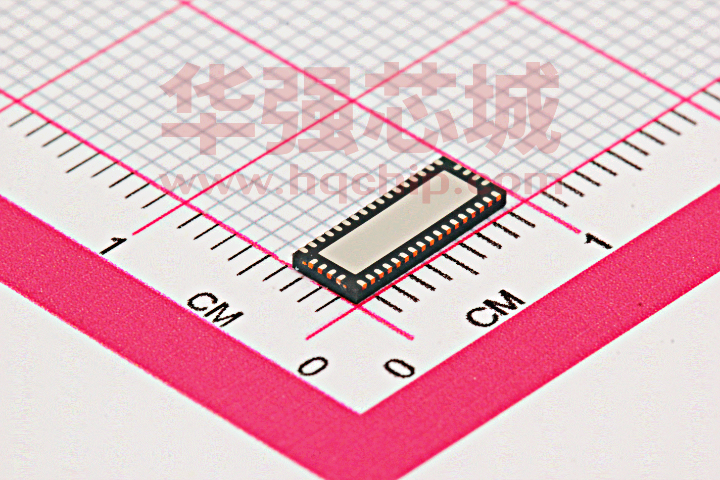
42-pin WQFN Package (9 mm x 3.5 mm, 0.5 mm
pitch)
HDMI 2.0 With Support for 4k2k up to 60 Hz
DVI 1.0 Signal Switching
DisplayPort 1.4 Signal Switching
General Purpose TMDS Signal Switching
General Purpose LVDS Signal Switching
General Purpose High-Speed Signal Switching
3 Description
The TS3DV642 is a 12 channel 1:2 or 2:1 bidirectional multiplexer/demultiplexer. The TS3DV642
operates from a 2.6 V to 4.5 V supply, making it
suitable for battery-powered applications. It offers low
and flat on-state resistance (RON) as well as low I/O
capacitance which allows it to achieve a typical
bandwidth of up to 7.5 GHz. The device provides the
high bandwidth necessary for HDMI and DisplayPort
applications.
The TS3DV642 offers a power-down mode, in which
all channels become Hi-Z and the device operates
with minimal power.
Device Information(1)
PART NUMBER
TS3DV642
PACKAGE
WQFN (42)
BODY SIZE (NOM)
9.00 mm × 3.50 mm
(1) For all available packages, see the orderable addendum at
the end of the datasheet.
Simplified Schematic
Primary HDMI Source
Channel
Display
Video Imaging
Processor
TS3DV642
Sideband
sso r
Secondary Source Sideband Channels:
DDC, CEC, & HPD
Channel
Gr ap
Secondary HDMI Source
T
Primary Source Sideband Channels:
DDC, CEC, & HPD
Data
1
An IMPORTANT NOTICE at the end of this data sheet addresses availability, warranty, changes, use in safety-critical applications,
intellectual property matters and other important disclaimers. PRODUCTION DATA.
�TS3DV642
SCDS343F – MAY 2013 – REVISED AUGUST 2018
www.ti.com
Table of Contents
1
2
3
4
5
6
7
8
Features ..................................................................
Applications ...........................................................
Description .............................................................
Revision History.....................................................
Pin Configuration and Functions .........................
Specifications.........................................................
1
1
1
2
4
6
6.1
6.2
6.3
6.4
6.5
6.6
6.7
6.8
6
6
6
6
7
8
8
9
Absolute Maximum Ratings ......................................
ESD Ratings ............................................................
Recommended Operating Conditions.......................
Thermal Information ..................................................
Electrical Characteristics...........................................
Dynamic Characteristics ...........................................
Switching Characteristics ..........................................
Typical Characteristics ..............................................
Parameter Measurement Information ................ 12
Detailed Description ............................................ 14
8.1 Overview ................................................................. 14
8.2 Functional Block Diagram ....................................... 14
8.3 Feature Description................................................. 14
8.4 Device Functional Modes........................................ 15
9
Application and Implementation ........................ 17
9.1 Application Information............................................ 17
9.2 Typical Application .................................................. 17
10 Power Supply Recommendations ..................... 22
11 Layout................................................................... 23
11.1 Layout Guidelines ................................................. 23
11.2 Layout Example .................................................... 24
12 Device and Documentation Support ................. 25
12.1
12.2
12.3
12.4
12.5
Receiving Notification of Documentation Updates
Community Resources..........................................
Trademarks ...........................................................
Electrostatic Discharge Caution ............................
Glossary ................................................................
25
25
25
25
25
13 Mechanical, Packaging, and Orderable
Information ........................................................... 25
4 Revision History
NOTE: Page numbers for previous revisions may differ from page numbers in the current version.
Changes from Revision E (June 2017) to Revision F
•
Page
Changed Figure 27, removed capacitors ............................................................................................................................ 21
Changes from Revision D (December 2015) to Revision E
Page
•
Changed Application From: DisplayPort 1.2a Signal Switching To: DisplayPort 1.4 Signal Switching.................................. 1
•
Added Test Condition of 4.05 GHZ at –35 dB to Xtalk in the Dynamic Characteristics table................................................ 8
•
Added Test Condition of 4.05 GHZ at –25 dB to OISO in the Dynamic Characteristics table............................................... 8
Changes from Revision C (November 2014) to Revision D
•
Page
Changed the storage temperature to the Absolute Maximum Ratings table ........................................................................ 6
Changes from Revision B (August 2013) to Revision C
Page
•
Added Handling Rating table, Feature Description section, Device Functional Modes, Application and
Implementation section, Power Supply Recommendations section, Layout section, Device and Documentation
Support section, and Mechanical, Packaging, and Orderable Information section. .............................................................. 1
•
Deleted row from ABS MAX table: Package thermal impedance .......................................................................................... 6
•
Added the Handling Ratings table, deleted the Tstg row Absolute Maximum ratings table and added to Handling
Ratings table. ......................................................................................................................................................................... 6
2
Submit Documentation Feedback
Copyright © 2013–2018, Texas Instruments Incorporated
Product Folder Links: TS3DV642
�TS3DV642
www.ti.com
SCDS343F – MAY 2013 – REVISED AUGUST 2018
Changes from Revision A (July 2013) to Revision B
Page
•
Changed Application From: HDMI 1.4/DVI 1.0 Signal Switching To: HDMI 1.4b with support for 4k2k up to 30 Hz ............ 1
•
Added Application: DVI 1.0 Signal Switching ......................................................................................................................... 1
•
Changed Application From: DisplayPort 1.2 Signal Switching To: DisplayPort 1.2a Signal Switching.................................. 1
•
Added Eye Pattern and Time Interval Error Histogram graphics, Figure 10 to Figure 13 ................................................... 10
Submit Documentation Feedback
Copyright © 2013–2018, Texas Instruments Incorporated
Product Folder Links: TS3DV642
3
�TS3DV642
SCDS343F – MAY 2013 – REVISED AUGUST 2018
www.ti.com
5 Pin Configuration and Functions
SDA_B
SCL_B
D0±A
SCL
3
36
D1+A
SDA
4
35
D1-A
D0+
5
34
D2+A
D0±
6
33
D2±A
D1+
7
32
D3+A
D1±
8
31
D3±A
NC
9
30
NC
D2+
10
29
D0+B
D2±
11
28
D0±B
D3+
12
27
D1+B
D3±
13
26
D1±B
HPD
14
25
D2+B
CEC
15
24
D2±B
SEL1
16
23
D3+B
SEL2
17
22
D3±B
39
37
40
2
Thermal
21
HPD_B
20
CEC_B
19
Pad
HPD_A
EN
41
D0+A
42
38
18
1
CEC_A
VCC
SDA_A
SCL_A
RUA Package
42 Pin WQFN With Exposed Thermal Pad
Top View
Not to scale
Pin Functions
PIN
NAME
NO.
TYPE
DESCRIPTION
VCC
1
Power
Supply Voltage
SEL1
16
I
Select Input 1
SEL2
17
I
Select Input 2
EN
2
I
Output Enable
D0+A
38
I/O
Port A, Channel 0, +ve signal
D0–A
37
I/O
Port A, Channel 0, –ve signal
D1+A
36
I/O
Port A, Channel 1, +ve signal
D1-A
35
I/O
Port A, Channel 1, –ve signal
D2+A
34
I/O
Port A, Channel 2, +ve signal
D2–A
33
I/O
Port A, Channel 2,–ve signal
D3+A
32
I/O
Port A, Channel 3, +ve signal
D3–A
31
I/O
Port A, Channel 3, –ve signal
SCL_A
42
I/O
Port A, DDC Clock
SDA_A
41
I/O
Port A, DDC Data
4
Submit Documentation Feedback
Copyright © 2013–2018, Texas Instruments Incorporated
Product Folder Links: TS3DV642
�TS3DV642
www.ti.com
SCDS343F – MAY 2013 – REVISED AUGUST 2018
Pin Functions (continued)
PIN
TYPE
DESCRIPTION
NAME
NO.
HPD_A
19
I/O
Port A, Hot Plug Detects
CEC_A
18
I/O
Port A, Consumer Electronics Control
D0+B
29
I/O
Port B, Channel 0, +ve signal
D0–B
28
I/O
Port B, Channel 0, –ve signal
D1+B
27
I/O
Port B, Channel 1, +ve signal
D1–B
26
I/O
Port B, Channel 1, –ve signal
D2+B
25
I/O
Port B, Channel 2, +ve signal
D2–B
24
I/O
Port B, Channel 2,–ve signal
D3+B
23
I/O
Port B, Channel 3, +ve signal
D3–B
22
I/O
Port B, Channel 3, –ve signal
SCL_B
40
I/O
Port B, DDC Clock
SDA_B
39
I/O
Port B, DDC Data
HPD_B
21
I/O
Port B, Hot Plug Detects
CEC_B
20
I/O
Port B, Consumer Electronics Control
D0+
5
I/O
Common Port, Channel 0, +ve signal
D0–
6
I/O
Common Port, Channel 0, –ve signal
D1+
7
I/O
Common Port, Channel 1, +ve signal
D1–
8
I/O
Common Port, Channel 1, –ve signal
D2+
10
I/O
Common Port, Channel 2, +ve signal
D2–
11
I/O
Common Port, Channel 2, –ve signal
D3+
12
I/O
Common Port, Channel 3, +ve signal
D3–
13
I/O
Common Port, Channel 3,–ve signal
SCL
3
I/O
Common Port, DDC Clock
SDA
4
I/O
Common Port, DDC Data
HPD
14
I/O
Common Port, Hot Plug Detects
CEC
15
I/O
Common Port, Consumer Electronics Control
9, 30
NC
No Connect
PowerPad
GND
NC
GND
Ground
Submit Documentation Feedback
Copyright © 2013–2018, Texas Instruments Incorporated
Product Folder Links: TS3DV642
5
�TS3DV642
SCDS343F – MAY 2013 – REVISED AUGUST 2018
www.ti.com
6 Specifications
6.1 Absolute Maximum Ratings
over operating free-air temperature range (unless otherwise noted) (1)
VCC
Supply voltage range
(2) (3) (4)
MIN
MAX
–0.5
5.5
UNIT
V
V
VI/O
Analog voltage range
All I/O
–0.5
5.5
VIN
Digital input voltage range (2) (3)
SEL1, SEL2, EN
–0.5
5.5
V
II/OK
Analog port diode current
VI/O < 0
–50
mA
IIK
Digital input clamp current
VIN < 0
II/O
On-state switch current (5)
Tstg
Storage temperature range
(1)
(2)
(3)
(4)
(5)
–50
mA
–128
128
mA
–65
150
°C
Stresses beyond those listed under Absolute Maximum Ratings may cause permanent damage to the device. These are stress ratings
only, which do not imply functional operation of the device at these or any other conditions beyond those indicated under Recommended
Operating Conditions. Exposure to absolute-maximum-rated conditions for extended periods may affect device reliability.
All voltages are with respect to ground, unless otherwise specified.
The input and output voltage ratings may be exceeded if the input and output clamp-current ratings are observed.
VI and VO are used to denote specific conditions for VI/O.
II and IO are used to denote specific conditions for II/O.
6.2 ESD Ratings
VALUE
Human body model (HBM), per ANSI/ESDA/JEDEC JS-001,
V(ESD)
Electrostatic discharge
(1)
Charged device model (CDM), per JEDEC specification JESD22-C101,
±1000
(2)
(1)
(2)
UNIT
±2000
V
JEDEC document JEP155 states that 500-V HBM allows safe manufacturing with a standard ESD control process.
JEDEC document JEP157 states that 250-V CDM allows safe manufacturing with a standard ESD control process.
6.3 Recommended Operating Conditions
over operating free-air temperature range (unless otherwise noted) (1)
VCC
Supply voltage
VI/O
Input/Output voltage
TA
Operating free-air temperature
(1)
MIN
MAX
2.6
4.5
UNIT
V
0
5.5
V
–40
85
°C
All unused control inputs of the device must be held at VDD or GND to ensure proper device operation. Refer to the TI application
report, Implications of Slow or Floating CMOS Inputs, literature number SCBA004.
6.4 Thermal Information
TS3DV642
THERMAL METRIC
(1)
RUA
UNIT
42 PINS
RθJA
Junction-to-ambient thermal resistance
31.5
°C/W
RθJC(top)
Junction-to-case (top) thermal resistance
16.2
°C/W
RθJB
Junction-to-board thermal resistance
5.5
°C/W
ψJT
Junction-to-top characterization parameter
0.2
°C/W
ψJB
Junction-to-board characterization parameter
5.4
°C/W
RθJC(bot)
Junction-to-case (bottom) thermal resistance
2.0
°C/W
(1)
6
For more information about traditional and new thermal metrics, see the Semiconductor and IC Package Thermal Metrics application
report.
Submit Documentation Feedback
Copyright © 2013–2018, Texas Instruments Incorporated
Product Folder Links: TS3DV642
�TS3DV642
www.ti.com
SCDS343F – MAY 2013 – REVISED AUGUST 2018
6.5 Electrical Characteristics
over operating free-air temperature range (unless otherwise noted)
PARAMETER
TEST CONDITIONS (1)
MIN TYP (2)
MAX
VCC = 3 V, 1.5 V ≤ VI/O ≤ VCC,
II/O = –40 mA
6.5
9.5
Ω
6
9.5
Ω
UNIT
PORT A
RON
ON-state resistance
D0 to D3
SCL, SDA, HPD, CEC
RON(flat) (3)
ON-state resistance
flatness
All I/O
VCC = 3 V, VI/O = 1.5 V and VCC,
II/O = –40 mA
ΔRON (4)
On-state resistance match
between high-speed
channels
D0 to D3
VCC = 3 V, 1.5 V ≤ VI/O ≤ VCC,
II/O = –40 mA
IOFF
Leakage under power off
All outputs
VCC = 0 V, VI/O = 0 to 3.6 V,
VIN = 0 V to 5.5 V
1.5
0.4
Ω
1
Ω
±10
µA
8.2
10.5
Ω
6
9.5
Ω
PORT B
D0 to D3
VCC = 3 V, 1.5 V ≤ VI/O ≤ VCC,
II/O = –40 mA
RON
ON-state resistance
RON(flat) (3)
ON-state resistance
flatness
All I/O
VCC = 3 V, VI/O = 1.5 V and VCC,
II/O = –40 mA
1.5
ΔRON (4)
On-state resistance match
between high-speed
channels
D0 to D3
VCC = 3 V, 1.5 V ≤ VI/O ≤ VCC,
II/O = –40 mA
0.4
IOFF
Leakage under power off
All outputs
VCC = 0 V, VI/O = 0 V to 3.6 V,
VIN = V to 5.5 V
SCL, SDA, HPD, CEC
Ω
1
Ω
±10
µA
DIGITAL INPUTS (SEL1, SEL2, EN)
VIH
High-level control input
voltage
SEL1, SEL2, EN
VIL
Low-level control input
voltage
SEL1, SEL2, EN
IIH
Digital input high leakage
current
SEL1, SEL2, EN
IIL
Digital input low leakage
current
SEL1, SEL2, EN
1.4
V
0.5
V
VCC = 3.6 V , VIN = VDD
±10
µA
VCC = 3.6 V, VIN = GND
±10
µA
SUPPLY
ICC
VCC supply current
VCC = 3.6 V, II/O = 0, Normal
Operation Mode, EN = H
50
µA
ICC, PD
VCC supply current in power-down mode
VCC = 3.6 V, II/O = 0, EN = L
6
µA
(1)
(2)
(3)
(4)
VI, VO, II, and IO refer to I/O pins, VIN refers to the control inputs.
All typical values are at VCC = 3.3 V (unless otherwise noted), TA = 25°C.
RON(FLAT) is the difference of RON in a given channel at specified voltages.
ΔRON is the difference of RON from center port to any other ports.
Submit Documentation Feedback
Copyright © 2013–2018, Texas Instruments Incorporated
Product Folder Links: TS3DV642
7
�TS3DV642
SCDS343F – MAY 2013 – REVISED AUGUST 2018
www.ti.com
6.6 Dynamic Characteristics
Over recommended operation free-air temperature range, VCC = 3.3V ± 0.3V (unless otherwise noted)
PARAMETER
TEST CONDITIONS
MIN
TYP (1)
MAX
UNIT
CIN
Digital input capacitance
f = 1 MHz, VIN = 0 V
6
pF
Coff
Switch OFF capacitance
f = 1 GHz, VI/O = 0 V, Output is open, Switch is OFF
0.3
pF
Con
Switch ON capacitance
f = 1 GHz, VI/O = 0 V, Output is open, Switch is ON
0.5
pF
RL = 50 Ω at 1.7 GHz (See Figure 17)
–40
RL = 50 Ω at 2.7 GHz (See Figure 17)
–40
RL = 50 Ω at 4.05 GHz (See Figure 17)
–35
RL = 50 Ω at 1.7 GHz (See Figure 18)
–23
RL = 50 Ω at 2.7 GHz (See Figure 18)
–28
RL = 50 Ω at 4.05 GHz (See Figure 18)
–25
Xtalk
OISO
Differential Crosstalk
Differential Off Isolation
IL
Insertion Loss
BW
Differential Bandwidth Port A
(–3 dB)
Port B
(1)
Port A at DC
–0.75
Port B at DC
–1
RL = 50 Ω, All channels (See Figure 19)
6.9
RL = 50 Ω, All channels (See Figure 19)
7.5
dB
dB
dB
GHz
All Typical Values are at VCC = 3.3 V (unless otherwise noted), TA = 25°C.
6.7 Switching Characteristics
over recommended operation free-air temperature range, VCC = 3.3 V± 0.3 V (unless otherwise noted)
PARAMETER
tON
(2)
tSWITCH
(3)
TEST CONDITIONS
Switch turn-on time
All I/O
See Figure 14
Switching time between channels
All I/O
See Figure 15
20
D0 to D3
Port A
tpd
Propagation Delay
D0 to D3
Port B
Inter-pair Skew
tSKEW
Intra-pair Skew
(1)
(2)
(3)
8
SCL, SDA,
HPD, CEC
Port B
Port A
Port B
MAX
UNIT
100
µs
µs
30
30
See Figure 16
40
SCL, SDA,
HPD, CEC
Port A
MIN TYP (1)
ps
30
Between +ve and –ve signals of
each Channel
D0 to D3
Between Channel 0, 1, 2, or 3
2
2
2
ps
6
All typical values are at VCC = 3.3 V (unless otherwise noted), TA = 25°C.
tON is the time it takes the output to recover after enabling switches
tSWITCH is the time it takes for the output to recover after the state is changed
Submit Documentation Feedback
Copyright © 2013–2018, Texas Instruments Incorporated
Product Folder Links: TS3DV642
�TS3DV642
www.ti.com
SCDS343F – MAY 2013 – REVISED AUGUST 2018
6.8 Typical Characteristics
Figure 1. Differential S21 vs Frequency for Port A
0
1.00E+05
1.00E+06
1.00E+07
1.00E+08
1.00E+09
Figure 2. Differential S21 vs Frequency for Port B
0
100000
1.00E+10
1000000
10000000
100000000
1E+09
1E+10
±10
-20
±20
±30
-40
dB
dB
±40
±50
-60
±60
-80
±70
±80
-100
±90
±100
-120
Frequency (Hz)
Frequency (Hz)
C001
C002
Figure 3. XTALK Port A
0
100000
1000000
10000000
100000000
Figure 4. XTALK Port B
1E+09
0
100000
1E+10
1000000
10000000
100000000
1E+09
1E+10
-10
-20
-20
-30
-40
dB
dB
-40
-50
-60
-60
-80
-70
-80
-100
-90
-100
-120
Frequency (Hz)
Frequency (Hz)
C003
Figure 5. Off-State Isolation (OISO) for Port A
C004
Figure 6. Off-State Isolation (OISO) for Port B
Submit Documentation Feedback
Copyright © 2013–2018, Texas Instruments Incorporated
Product Folder Links: TS3DV642
9
�TS3DV642
SCDS343F – MAY 2013 – REVISED AUGUST 2018
www.ti.com
Typical Characteristics (continued)
Figure 7. Return Loss (S11) Characteristics of TS3DV642
Figure 8. Eye Pattern: 6.0 Gbps Port A, D1+ to D1+A, D1- to
D1-A (Only One Channel Measured at a Time)
Figure 9. Eye Pattern: 6.0 Gbps, No Device Through Path (Only One Channel Measured at a Time)
Figure 10. Eye Pattern and Time Interval Error Histogram: 3.4 Gbps Port A, With Device
10
Submit Documentation Feedback
Copyright © 2013–2018, Texas Instruments Incorporated
Product Folder Links: TS3DV642
�TS3DV642
www.ti.com
SCDS343F – MAY 2013 – REVISED AUGUST 2018
Figure 11. Eye Pattern and Time Interval Error Histogram: 3.4 Gbps, No Device Through Path
Figure 12. Eye Pattern and Time Interval Error Histogram: 3.4 Gbps Port B, With Device
Figure 13. Eye Pattern and Time Interval Error Histogram: 3.4 Gbps Port B, No Device
Submit Documentation Feedback
Copyright © 2013–2018, Texas Instruments Incorporated
Product Folder Links: TS3DV642
11
�TS3DV642
SCDS343F – MAY 2013 – REVISED AUGUST 2018
www.ti.com
7 Parameter Measurement Information
VCC
RL
50 Ω
CL
4 pF
VCOM
VCC
*CL includes probe, cable, and board
capacitance
Port A
VCOM
2.6 V
Port B
+
CL
EN
RL
50%
0
EN
CL
tON
RL
VOH
Switch
Output
Control
50%
VOL
Input
Figure 14. Switch Turn-On Time (tON)
VCC
RL
50 Ω
CL
4 pF
V COM
VCC
*CL includes probe, cable, and board
capacitance
Port A
VCOM
CL
Port B
+
SEL1/SEL2
CL
RL
2.6 V
SEL1/SEL2
RL
50%
0
tON
Switch
Output
Control
Input
VOH
50%
VOL
Figure 15. Switching Time Between Channels (tSWITCH)
3V
Input
50%
50%
0
tPLH
Output
tPLH
50%
tpd = (tPLH + tPLH) / 2
VOH
50%
VOL
Figure 16. Propagation Delay (tpd)
12
Submit Documentation Feedback
Copyright © 2013–2018, Texas Instruments Incorporated
Product Folder Links: TS3DV642
�TS3DV642
www.ti.com
SCDS343F – MAY 2013 – REVISED AUGUST 2018
Parameter Measurement Information (continued)
VDD
Network Analyzer
TS3DV642
RS
RT
VS
RT
Channel ON
VOUT
SEL = H or L
RS = RT = 50Ω
NC
VS
RT
SEL
GND
VS = -10dBm (200mV at 50Ω Load)
VDC_BIAS = 1 V
RT
Control
Input
Figure 17. Crosstalk (Xtalk)
VCC
Network Analyzer
TS3DV642
RS
VOUT+
RT
VS
RS
RT
VOUT-
VS
SEL
GND
RT
Channel OFF
SEL = H or L
RS = RT = 50Ω
VS = -10dBm (200mV at 50Ω Load)
VDC_BIAS = 1 V
RT
Control
Input
Figure 18. Differential Off-Isolation (OISO)
VDD
VOUT+
Network Analyzer
TS3DV642
RS
VS
RT
VOUT-
RS
VS
RT
GND
Channel ON
SEL = H or L
RS = RT = 50Ω
VS = -10dBm (200mV at 50Ω Load)
VDC_BIAS = 1 V
RT
RT
Control
Input
Figure 19. Differential Bandwidth (BW)
Submit Documentation Feedback
Copyright © 2013–2018, Texas Instruments Incorporated
Product Folder Links: TS3DV642
13
�TS3DV642
SCDS343F – MAY 2013 – REVISED AUGUST 2018
www.ti.com
8 Detailed Description
8.1 Overview
TS3DV642 is a 12-channel 1:2 or 2:1 bidirectional multiplexer/demultiplexer. The TS3DV642 operates from a 2.6
to 4.5 V supply, making it suitable for battery-powered applications. It offers low and flat on-state resistance as
well as low I/O capacitance which allows it to achieve a typical bandwidth of up to 7.5 GHz. The device provides
the high bandwidth necessary for HDMI and DisplayPort applications.
8.2 Functional Block Diagram
TS3DV642
SEL1,
SEL2,
EN
D0+
D0+A
D0+B
CEC
CEC_A
CEC_B
8.3 Feature Description
The TS3DV642 is based on proprietary TI technology which uses FET switches driven by a high-voltage
generated from an integrated charge-pump to achieve a low on-state resistance. TS3DV642 has 12-channel
bidirectional switches with a high bandwidth (~ 7.5 GHz). TS3DV642 uses an extremely low power technology
and uses only 50 µA ICC in active mode. The device has integrated ESD that can support up to 2-kV HumanBody Model (HBM) and 1-kV Charge Device Model (CDM). TS3DV642 is offered in a 42-pin QFN package (9
mm x 3.5 mm) with 0.5 mm pitch. The device can support analog I/O signal in 0 to 5 V range. TS3DV642 also
has a special feature that prevents the device from back-powering when the VCC supply is not available and an
analog signal is applied on the I/O pin. In this situation this special feature prevents leakage current in the device.
The TS3DV642 is not designed for passing signals with negative swings; the high-speed signals need to be
properly DC biased (usually ~1 V) before being passed to the TS3DV642. The differential S21 characteristics as
a function of frequency for Port A and Port B are shown in Figure 1 and Figure 2, respectively. The figures show
a differential bandwidth of 6.7 GHz and 7.7 GHz for Port A and Port B, respectively. The cross-talk (XTALK)
characteristics as a function of frequency are shown in Figure 3 and Figure 4, respectively. The off-state isolation
(OISO) characteristics for Port A and Port B are shown in Figure 5 and Figure 6, respectively. The return loss
14
Submit Documentation Feedback
Copyright © 2013–2018, Texas Instruments Incorporated
Product Folder Links: TS3DV642
�TS3DV642
www.ti.com
SCDS343F – MAY 2013 – REVISED AUGUST 2018
Feature Description (continued)
characteristics (S11) are shown in Figure 7. The eye pattern and Time Interval Error (TIE) histogram at 3.4 Gbps
(for HDMI 1.4 applications) with TS3DV642 in path for Port A is shown in Figure 10. The eye pattern and Time
Interval Error (TIE) histogram at 3.4 Gbps through path (no TS3DV642) for Port A is shown in Figure 11. The eye
pattern and Time Interval Error (TIE) histogram at 3.4 Gbps (for HDMI 1.4 applications) with TS3DV642 in path
for Port B is shown in Figure 12. The eye pattern and Time Interval Error (TIE) histogram at 3.4 Gbps through
path (no TS3DV642) for Port A is shown in Figure 13. The eye pattern at 6.0 Gbps (for HDMI 2.0 applications)
with TS3DV642 in path for Port A is shown in Figure 8. The eye pattern at 6.0 Gbps (for HDMI 2.0 applications)
through path (no TS3DV642) for Port A is shown in Figure 9. Note that the eye patterns are measured with only
one channel on at a time.
8.4 Device Functional Modes
D0+
D0+A
D0-
D0-A
D1+
D1+A
D1-
D1-A
D2+
D2+A
D2-
D2-A
D3+
D3-
D3+A
D3-A
D0+B
D0-B
D1+B
D1-B
D2+B
D2-B
D3+B
D3-B
SCL
SCL_A
SDA
SDA_A
HPD
HPD_A
CEC
CEC_A
SCL_B
SDA_B
HPD_B
CEC_B
SEL1
SEL2
Control Logic
EN
Figure 20. Logic Diagram
Submit Documentation Feedback
Copyright © 2013–2018, Texas Instruments Incorporated
Product Folder Links: TS3DV642
15
�TS3DV642
SCDS343F – MAY 2013 – REVISED AUGUST 2018
www.ti.com
Device Functional Modes (continued)
Table 1 lists the device functions for the TS3DV642 device.
Table 1. Functional Table
16
EN
SEL1
SEL2
FUNCTION
L
X
X
Switch disabled. All channels are Hi-Z.
H
L
L
Channel D0+/D0– to D0+A/D0–A is ON. All the other channels (D1+/D1-,
D2+/D2-, D3+/D3-, SCL, SDA, HPD, CEC) are Hi-Z.
H
L
H
Channel D0+/D0– to D0+B/D0–B is ON. All the other channels (D1+/D1-,
D2+/D2-, D3+/D3-, SCL, SDA, HPD, CEC) are Hi-Z.
H
H
L
All A channels are enabled. All B channels are Hi-Z.
H
H
H
All B channels are enabled. All A channels are Hi-Z.
Submit Documentation Feedback
Copyright © 2013–2018, Texas Instruments Incorporated
Product Folder Links: TS3DV642
�TS3DV642
www.ti.com
SCDS343F – MAY 2013 – REVISED AUGUST 2018
9 Application and Implementation
NOTE
Information in the following applications sections is not part of the TI component
specification, and TI does not warrant its accuracy or completeness. TI’s customers are
responsible for determining suitability of components for their purposes. Customers should
validate and test their design implementation to confirm system functionality.
9.1 Application Information
TS3DV642 can be used for two typical DisplayPort applications. Figure 21 describes a DisplayPort (DP)
application where TS3DV642 is used to switch between two different graphic & memory controllers on a single
DP connector. Figure 24 shows a docking application where TS3DV642 is used to switch signals from a single
graphic and memory controller to a display port and docking station connector. Note that the TS3DV642 is not
designed for passing signals with negative swings; the high-speed signals need to be properly DC biased
(usually ~1 V from the graphic controller side) before being passed to the TS3DV642.
9.2 Typical Application
9.2.1 Display Port (DP) Application
Display port (DP) application with TS3DV642 used to switch between two different graphic & memory controllers
on a single DP connector
VCC
0.1 µF
VCC
TS3DV642
D0+A
ML_0-A
ML_1+A
ML_1-A
ML_2+A
Graphic and Memory
Controller A
D1+A
D2+A
ML_2-A
D2-A
D3+A
ML_3-A
D3-A
AUX+A
SCL_A
ML_0+B
ML_0-B
ML_1+B
ML_1-B
ML_2+B
VCC
D1-A
ML_3+A
AUX-A
HPDA
Graphic and Memory
Controller B
D0-A
SDA_A
HPD_A
D0+B
D0-B
D0+
D0±
D1+
D1±
D2+
D2±
D3+
D1+B
D3±
D1-B
SCL
D2+B
SDA
ML_2-B
D2-B
ML_3+B
HPD
D3+B
ML_3-B
D3-B
AUX+B
SCL_B
AUX-B
HPDB
SDA_B
HPD_B
VCC
ML_0+
ML_0ML_1+
ML_1ML_2+
ML_2ML_3+
DisplayPort
Connector
ML_3AUX+
AUXHPD
VCC
SEL1
SEL2
Figure 21. Display Port Schematic
Submit Documentation Feedback
Copyright © 2013–2018, Texas Instruments Incorporated
Product Folder Links: TS3DV642
17
�TS3DV642
SCDS343F – MAY 2013 – REVISED AUGUST 2018
www.ti.com
Typical Application (continued)
9.2.1.1 Design Requirements
Table 2. Design parameters for Display Port application
Design parameter
Example value
VCC
2.6 V to 4.5 V
VCC decoupling capacitor
0.1 µF
MainLink (ML) and AUX coupling capacitor
75 nF to 200 nF
AUX Pull-up / Pull-down resistors
10 kΩ to 100 kΩ
Pull-up / Pull-down resistors for SEL1 / SEL2 pins
10 kΩ
9.2.1.2 Detailed Design Procedure
The TS3DV642 is designed to operate with 2.6 V – 4.5 V power supply. The wide power supply range allows
flexibility for battery powered applications. If a higher power supply is used in the system, a voltage regulator can
be used to bring down the voltage to 2.6 V – 4.5 V range. Decoupling capacitors may be used to reduce noise
and improve power supply integrity. AC coupling capacitors in 75 nF – 200 nF range must be placed on the
MainLink (ML) and AUX lanes. In this particular application the AC coupling capacitors are shown on the
connector side. The AC coupling capacitors may also be placed on the signal path on controller side. The AUX+
line must be pulled-down weakly through a resistor to ground and the AUX– line must be pulled-up weakly
through a resistor to VCC.
9.2.1.3 Application Curves
Figure 22. Eye Pattern: 6.0 Gbps Port A, D1+ to D1+A, D1to D1-A (Only One Channel Measured at a Time)
18
Figure 23. Eye Pattern: 6.0 Gbps, No Device Through Path
(Only One Channel Measured at a Time)
Submit Documentation Feedback
Copyright © 2013–2018, Texas Instruments Incorporated
Product Folder Links: TS3DV642
�TS3DV642
www.ti.com
SCDS343F – MAY 2013 – REVISED AUGUST 2018
9.2.2 Docking Application
Docking Application with TS3DV642 used to switch signals from a single graphic and memory controller to a
display port and docking station connector.
VCC
0.1 µF
VCC
VCC
TS3DV642
Graphic and Memory
Controller
D0+A
D0-A
D1+A
D1-A
D2+A
ML_0+B
ML_0-B
ML_1+B
ML_1-B
ML_2+B
ML_2-B
D0+
D2-A
D0-
D3+A
D1+
D3-A
D1-
SCL_A
D2+
SDA_A
HPD_A
D2-
ML_3+B
D3+
ML_3-B
D3-
AUX+B
SCL
AUX-B
SDA
HPDB
HPD
D0+B
D0-B
D1+B
D1-B
D2+B
D2-B
D3+B
VCC
D3-B
VCC
SCL_B
SDA_B
HPD_B
VCC
ML_0+A
ML_0-A
ML_1+A
ML_1-A
ML_2+A
DisplayPort
Connector
ML_2-A
ML_3+A
ML_3-A
AUX+A
AUX-A
HPDA
ML_0+B
ML_0-B
ML_1+B
ML_1-B
ML_2+B
ML_2-B
Docking
Station
ML_3+B
ML_3-B
AUX+B
AUX-B
HPDB
SEL1
SEL2
Figure 24. Docking Application Schematic
9.2.2.1 Design Requirements
Table 3. Design parameters for docking application
Design parameter
Example value
VCC
2.6 V to 4.5 V
VCC decoupling capacitor
0.1 µF
MainLink (ML) and AUX coupling capacitor
75 nF to 200 nF
AUX Pull-up / Pull-down resistors
10 kΩ to 100 kΩ
Pull-up / Pull-down resistors for SEL1 / SEL2 pins
10 kΩ
Submit Documentation Feedback
Copyright © 2013–2018, Texas Instruments Incorporated
Product Folder Links: TS3DV642
19
�TS3DV642
SCDS343F – MAY 2013 – REVISED AUGUST 2018
www.ti.com
9.2.2.2 Detailed Design Procedure
The TS3DV642 is designed to operate with 2.6 V – 4.5 V power supply. The wide power supply range allows
flexibility for battery powered applications. If a higher power supply is used in the system, a voltage regulator can
be used to bring down the voltage to 2.6 V – 4.5 V range. Decoupling capacitors may be used to reduce noise
and improve power supply integrity. AC coupling capacitors in 75 nF – 200 nF range must be placed on the
MainLink (ML) and AUX lanes. In this particular application the AC coupling capacitors are shown on the
connector side. The AC coupling capacitors may also be placed on the signal path on controller side. The AUX+
line must be pulled-down weakly through a resistor to ground and the AUX– line must be pulled-up weakly
through a resistor to VCC.
9.2.2.3 Application Curves
Figure 25. Eye Pattern: 6.0 Gbps Port A, D1+ to D1+A, D1to D1-A (Only One Channel Measured at a Time)
20
Figure 26. Eye Pattern: 6.0 Gbps, No Device Through Path
(Only One Channel Measured at a Time)
Submit Documentation Feedback
Copyright © 2013–2018, Texas Instruments Incorporated
Product Folder Links: TS3DV642
�TS3DV642
www.ti.com
SCDS343F – MAY 2013 – REVISED AUGUST 2018
9.2.3 HDMI Application
HDMI Application with TS3DV642 used to switch signals from a single graphic and memory controller to a two
HDMI connectors.
VCC
0.1 µF
5V
5V
Graphic &
Memory
Controller
VCC
2k
2k
TS3DV642
D0+A
TMDS_0+
TMDS_0TMDS_1+
TMDS_1TMDS_2+
TMDS_2TMDS_3+
TMDS_3-
D0+
D0D1+
D1D2+
D2D3+
D0-A
D1+A
D1-A
D2+A
D2-A
D3+A
D3-A
SCL_A
SDA_A
HPD_A
CEC_A
D3SCL
SDA
HPD
CEC
HPD
CEC
VCC
VCC
D3-B
SCL_B
SDA_B
HPD_B
CEC_B
DDCCLK_B
DDCDAT_B
HPD_B
CEC_B
SEL1
SEL2
D0-B
D1+B
D1-B
D2+B
D2-B
D3+B
HDMI
Connector 1
DDCCLK_A
DDCDAT_A
HPD_A
CEC_A
TMDS_0+B
TMDS_0-B
TMDS_1+B
TMDS_1-B
TMDS_2+B
TMDS_2-B
TMDS_3+B
TMDS_3-B
D0+B
DDCCLK
DDCDAT
TMDS_0+A
TMDS_0-A
TMDS_1+A
TMDS_1-A
TMDS_2+A
TMDS_2-A
TMDS_3+A
TMDS_3-A
HDMI
Connector 2
Figure 27. HDMI Application Schematic
9.2.3.1 Design Requirements
Table 4. Design Parameters for HDMI Application
Design parameter
Example value
VCC
2.6 V to 4.5 V
VCC decoupling capacitor
0.1 µF
DDC Pull-up resistors
2 kΩ to 5 V
Pull-up / Pull-down resistors for SEL1 / SEL2 pins
10 kΩ
HPD Pull-down resistor
100 kΩ
9.2.3.2 Detailed Design Procedure
The TS3DV642 is designed to operate with 2.6 V – 4.5 V power supply. The wide power supply range allows
flexibility for battery powered applications. If a higher power supply is used in the system, a voltage regulator can
be used to bring down the voltage to 2.6 V – 4.5 V range. Decoupling capacitors may be used to reduce noise
and improve power supply integrity. Pull-up resistors to 5 V must be placed on the source side DDC clock and
data lines according to the HDMI standard. A weak pull-down resistor must be placed on the source side HPD
line.
Submit Documentation Feedback
Copyright © 2013–2018, Texas Instruments Incorporated
Product Folder Links: TS3DV642
21
�TS3DV642
SCDS343F – MAY 2013 – REVISED AUGUST 2018
www.ti.com
9.2.3.3 Application Curves
Figure 28. Eye Pattern: 6 Gbps Port A, D1+ to D1+A, D1- to
D1-A (Only One Channel Measured at a Time)
Figure 29. Eye Pattern: 6 Gbps, No Device Through Path
(Only One Channel Measured at a Time)
10 Power Supply Recommendations
VCC should be in the range of 2.6 V to 4.5 V. Voltage levels above those listed in the Absolute Ratings table
should not be used. Decoupling capacitors may be used to reduce noise and improve power supply integrity.
There are no power sequence requirements for the TS3DV642.
22
Submit Documentation Feedback
Copyright © 2013–2018, Texas Instruments Incorporated
Product Folder Links: TS3DV642
�TS3DV642
www.ti.com
SCDS343F – MAY 2013 – REVISED AUGUST 2018
11 Layout
11.1 Layout Guidelines
To ensure reliability of the device, the following commonly used printed-circuit board layout guidelines are
recommended:
• Decoupling capacitors should be used between power supply pin and ground pin to ensure low impedance to
reduce noise To achieve a low impedance over a wide frequency range use capacitors with a high selfresonance frequency.
• ESD and EMI protection devices (if used) should be placed as close as possible to the connector.
• Short trace lengths should be used to avoid excessive loading.
• To minimize the effects of crosstalk on adjacent traces, keep the traces at least two times the trace width
apart.
• Separate high-speed signals from low-speed signals and digital from analog signals
• Avoid right-angle bends in a trace and try to route them at least with two 45° corners.
• The high-speed differential signal traces should be routed parallel to each other as much as possible. The
traces are recommended to be symmetrical.
• A solid ground plane should be placed next to the high-speed signal layer. This also provides an excellent
low-inductance path for the return current flow.
Submit Documentation Feedback
Copyright © 2013–2018, Texas Instruments Incorporated
Product Folder Links: TS3DV642
23
�TS3DV642
SCDS343F – MAY 2013 – REVISED AUGUST 2018
www.ti.com
11.2 Layout Example
MCU
40
39
42
3
36
SDA
4
35
D0+
5
34
D0-
6
33
D1+
7
32
D1-
8
31
9
30
D2+
10
29
D2-
11
28
D3+
12
27
D3-
13
26
HPD
14
25
CEC
15
24
16
23
17
22
HDMI Connector A
21
37
SCL
19
38
2
20
1
18
HDMI
controller
41
TS3DV642 application with a single controller interfacing with two HDMI connectors.
GPIOA
GPIOB
GPIOC
: VIA to GND
: VIA to signal plane
HDMI Connector B
Figure 30. Layout Example
24
Submit Documentation Feedback
Copyright © 2013–2018, Texas Instruments Incorporated
Product Folder Links: TS3DV642
�TS3DV642
www.ti.com
SCDS343F – MAY 2013 – REVISED AUGUST 2018
12 Device and Documentation Support
12.1 Receiving Notification of Documentation Updates
To receive notification of documentation updates, navigate to the device product folder on ti.com. In the upper
right corner, click on Alert me to register and receive a weekly digest of any product information that has
changed. For change details, review the revision history included in any revised document.
12.2 Community Resources
The following links connect to TI community resources. Linked contents are provided "AS IS" by the respective
contributors. They do not constitute TI specifications and do not necessarily reflect TI's views; see TI's Terms of
Use.
TI E2E™ Online Community TI's Engineer-to-Engineer (E2E) Community. Created to foster collaboration
among engineers. At e2e.ti.com, you can ask questions, share knowledge, explore ideas and help
solve problems with fellow engineers.
Design Support TI's Design Support Quickly find helpful E2E forums along with design support tools and
contact information for technical support.
12.3 Trademarks
E2E is a trademark of Texas Instruments.
All other trademarks are the property of their respective owners.
12.4 Electrostatic Discharge Caution
These devices have limited built-in ESD protection. The leads should be shorted together or the device placed in conductive foam
during storage or handling to prevent electrostatic damage to the MOS gates.
12.5 Glossary
SLYZ022 — TI Glossary.
This glossary lists and explains terms, acronyms, and definitions.
13 Mechanical, Packaging, and Orderable Information
The following pages include mechanical, packaging, and orderable information. This information is the most
current data available for the designated devices. This data is subject to change without notice and revision of
this document. For browser-based versions of this data sheet, refer to the left-hand navigation.
Submit Documentation Feedback
Copyright © 2013–2018, Texas Instruments Incorporated
Product Folder Links: TS3DV642
25
�PACKAGE OPTION ADDENDUM
www.ti.com
24-Aug-2018
PACKAGING INFORMATION
Orderable Device
Status
(1)
TS3DV642A0RUAR
ACTIVE
Package Type Package Pins Package
Drawing
Qty
WQFN
RUA
42
3000
Eco Plan
Lead/Ball Finish
MSL Peak Temp
(2)
(6)
(3)
Green (RoHS
& no Sb/Br)
CU NIPDAU | Call TI
Level-3-260C-168 HR
Op Temp (°C)
Device Marking
(4/5)
-40 to 85
SD642A0
(1)
The marketing status values are defined as follows:
ACTIVE: Product device recommended for new designs.
LIFEBUY: TI has announced that the device will be discontinued, and a lifetime-buy period is in effect.
NRND: Not recommended for new designs. Device is in production to support existing customers, but TI does not recommend using this part in a new design.
PREVIEW: Device has been announced but is not in production. Samples may or may not be available.
OBSOLETE: TI has discontinued the production of the device.
(2)
RoHS: TI defines "RoHS" to mean semiconductor products that are compliant with the current EU RoHS requirements for all 10 RoHS substances, including the requirement that RoHS substance
do not exceed 0.1% by weight in homogeneous materials. Where designed to be soldered at high temperatures, "RoHS" products are suitable for use in specified lead-free processes. TI may
reference these types of products as "Pb-Free".
RoHS Exempt: TI defines "RoHS Exempt" to mean products that contain lead but are compliant with EU RoHS pursuant to a specific EU RoHS exemption.
Green: TI defines "Green" to mean the content of Chlorine (Cl) and Bromine (Br) based flame retardants meet JS709B low halogen requirements of