TS5A23157-Q1
SCDS252B – JULY 2007 – REVISED JUNE 2021
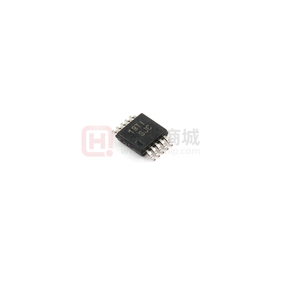
TS5A23157-Q1 Dual 15-Ω SPDT Analog Switch
1 Features
3 Description
•
•
The TS5A23157-Q1 is a dual, single-pole, doublethrow (SPDT) analog switch designed to operate from
1.65 V to 5.5 V. This device can handle both digital
and analog signals. The device can transmit signals
up to 5.5 V (peak) in either direction.
•
•
•
•
•
•
•
•
•
Qualified for automotive applications
AEC-Q100 qualified with the following results:
– Device temperature grade 1: –40°C to 125°C
– Device HBM ESD classification level H2
– Device CDM ESD classification level C4B
Functional safety-capable
– Documentation available to aid functional safety
system design
Customer-specific configuration control can be
supported along with major-change approval
Specified break-before-make switching
Low ON-state resistance (15 Ω)
Control inputs are 5-V tolerant
Low charge injection
Excellent ON-resistance matching
Low total harmonic distortion
1.8-V to 5.5-V single-supply operation
2 Applications
•
•
•
•
Sample-and-hold circuits
Battery-powered equipment
Audio and video signal routing
Communication circuits
For the most current package and ordering
information, see the Package Option Addendum at
the end of this document, or see the TI Web site at
www.ti.com.
Table 3-1. Device Information(1)
PART NUMBER
PACKAGE
BODY SIZE (NOM)
TS5A23157-Q1
VSSOP (10)
3.00 mm × 3.00 mm
(1)
For all available packages, see the package option
addendum at the end of the data sheet.
IN1
1
10
NO1
2
9
NC1
GND
3
8
V+
NO2
4
7
NC2
IN2
5
6
COM2
COM1
TS5A23157-Q1 Functional Diagram
An IMPORTANT NOTICE at the end of this data sheet addresses availability, warranty, changes, use in safety-critical applications,
intellectual property matters and other important disclaimers. PRODUCTION DATA.
�TS5A23157-Q1
www.ti.com
SCDS252B – JULY 2007 – REVISED JUNE 2021
Table of Contents
1 Features............................................................................1
2 Applications..................................................................... 1
3 Description.......................................................................1
4 Revision History.............................................................. 2
5 Pin Configurations and Functions.................................3
6 Specifications.................................................................. 4
6.1 Absolute Maximum Ratings........................................ 4
6.2 Electrical Characteristics for 5-V Supply.....................5
6.3 Electrical Characteristics for 3.3-V Supply..................7
6.4 Electrical Characteristics for 2.5-V Supply..................8
6.5 Electrical Characteristics for 1.8-V Supply..................9
6.6 Typical Characteristics.............................................. 10
7 Parameter Description.................................................. 11
8 Parameter Measurement Information.......................... 12
9 Function and Summary of Characteristics................. 16
10 Detailed Description....................................................17
10.1 Overview................................................................. 17
10.2 Functional Block Diagram....................................... 17
10.3 Feature Description.................................................17
10.4 Device Functional Modes........................................17
11 Application and Implementation................................ 18
11.1 Application Information............................................18
11.2 Typical Application.................................................. 18
11.3 Design Requirements..............................................18
11.4 Detailed Design Procedure..................................... 19
11.5 Application Performance Plots................................ 19
12 Power Supply Recommendations..............................19
13 Layout...........................................................................20
13.1 Layout Guidelines................................................... 20
13.2 Layout Example...................................................... 21
14 Device and Documentation Support..........................22
14.1 Receiving Notification of Documentation Updates..22
14.2 Support Resources................................................. 22
14.3 Trademarks............................................................. 22
14.4 Electrostatic Discharge Caution..............................22
14.5 Glossary..................................................................22
15 Mechanical, Packaging, and Orderable
Information.................................................................... 22
15.1 Ordering Information............................................... 22
4 Revision History
NOTE: Page numbers for previous revisions may differ from page numbers in the current version.
Changes from Revision A (February 2013) to Revision B (June 2021)
Page
• Updated the numbering format for tables, figures, and cross-references throughout the document..................1
• Added functional safety-capable information to the Features section................................................................ 1
2
Submit Document Feedback
Copyright © 2021 Texas Instruments Incorporated
Product Folder Links: TS5A23157-Q1
�TS5A23157-Q1
www.ti.com
SCDS252B – JULY 2007 – REVISED JUNE 2021
5 Pin Configurations and Functions
IN1
1
10
COM1
NO1
2
9
NC1
GND
3
8
V+
NO2
4
7
NC2
IN2
5
6
COM2
Not to scale
Figure 5-1. DGS VSSOP (16) Top View
Table 5-1. Pin Functions
PIN
Type
DESCRIPTION
NAME
NO.
COM1
10
I/O
Common
COM2
6
I/O
Common
GND
3
P
Ground
IN1
1
I
Digital control to connect COM to NO or NC
IN2
5
I
Digital control to connect COM to NO or NC
NC1
9
I/O
Normally closed
NC2
7
I/O
Normally closed
NO1
2
I/O
Normally open
NO2
4
I/O
Normally open
V+
8
P
Power supply
1. I = input, O = output, I/O = input and output, P = power.
Submit Document Feedback
Copyright © 2021 Texas Instruments Incorporated
Product Folder Links: TS5A23157-Q1
3
�TS5A23157-Q1
www.ti.com
SCDS252B – JULY 2007 – REVISED JUNE 2021
6 Specifications
6.1 Absolute Maximum Ratings
over operating free-air temperature range (unless otherwise noted)
MIN
MAX
V+
Supply voltage range(1)
–0.5
6.5
V
VNC
VNO
VCOM
Analog voltage range(1) (2) (3)
–0.5
V+ + 0.5
V
II/OK
Analog port diode current
VNC, VNO, VCOM < 0 or VNC, VNO, VCOM > V+
±50
mA
INC
INO
ICOM
On-state switch current
VNC, VNO, VCOM = 0 to V+
±50
mA
VIN
Digital input voltage range(1) (2)
IIK
Digital input clamp current
–0.5
VIN < 0
Continuous current through V+ or GND
θJA
Package thermal impedance(4)
Tstg
Storage temperature range
ESD
(1)
(2)
(3)
(4)
4
Electrostatic discharge rating
6.5
V
–50
mA
±100
165.36
–65
Human-body model H2
Charged-device model C4B
UNIT
mA
°C/W
150
°C
2
kV
750
V
All voltages are with respect to ground, unless otherwise specified.
The input and output voltage ratings may be exceeded if the input and output clamp-current ratings are observed.
This value is limited to 5.5 V maximum.
The package thermal impedance is calculated in accordance with JESD 51-7.
Submit Document Feedback
Copyright © 2021 Texas Instruments Incorporated
Product Folder Links: TS5A23157-Q1
�TS5A23157-Q1
www.ti.com
SCDS252B – JULY 2007 – REVISED JUNE 2021
6.2 Electrical Characteristics for 5-V Supply
V+ = 4.5 V to 5.5 V, TA = –40°C to 125°C (unless otherwise noted)
PARAMETER
SYMBOL
TEST CONDITIONS
TA
V+
MIN
TYP(1)
MAX
UNIT
Analog Switch
Analog signal range
VCOM,
VNO, VNC
ON-state resistance
ron
0 ≤ VNO or VNC ≤ V+,
ICOM = –30 mA,
Switch ON,
See Figure 8-1
Full
4.5 V
ON-state resistance
match between
channels
Δron
VNO or VNC = 3.15 V,
ICOM = –30 mA,
Switch ON,
See Figure 8-1
25°C
4.5 V
0.15
Ω
ON-state resistance
flatness
ron(flat)
0 ≤ VNO or VNC ≤ V+,
ICOM = –30 mA,
Switch ON,
See Figure 8-1
25°C
4.5 V
4
Ω
NC, NO
OFF leakage current
INC(OFF), VNC or VNO = 0 to V+,
INO(OFF) VCOM = 0 to V+,
Switch OFF,
See Figure 8-2
25°C
NC, NO
ON leakage current
INC(ON),
INO(ON)
VNC or VNO = 0 to V+,
VCOM = Open,
Switch ON,
See Figure 8-2
25°C
COM
ON leakage current
ICOM(ON)
VNC or VNO = Open,
VCOM = 0 to V+,
Switch ON,
See Figure 8-2
25°C
0
Full
Full
Full
5.5 V
5.5 V
5.5 V
–1
0.05
V+
V
15
Ω
1
–1
1
–0.1
0.1
–1
1
–0.1
0.1
–1
1
μA
μA
μA
Digital Inputs (IN1, IN2)(2)
Input logic high
VIH
Input logic low
VIL
Input leakage
current
IIH, IIL
Full
V+ × 0.7
V
Full
VIN = 5.5 V or 0
25°C
Full
V+ × 0.3
5.5 V
–1
–1
0.05
1
1
V
μA
Submit Document Feedback
Copyright © 2021 Texas Instruments Incorporated
Product Folder Links: TS5A23157-Q1
5
�TS5A23157-Q1
www.ti.com
SCDS252B – JULY 2007 – REVISED JUNE 2021
6.2 Electrical Characteristics for 5-V Supply (continued)
V+ = 4.5 V to 5.5 V, TA = –40°C to 125°C (unless otherwise noted)
PARAMETER
SYMBOL
TEST CONDITIONS
TA
V+
MIN
TYP(1)
MAX
UNIT
Dynamic
Turnon time
tON
VNC = GND and VNO = V+,
or
VNC = V+ and VNO = GND,
RL = 500 Ω,
CL = 50 pF,
See Figure 8-4
Full
4.5 V
to
5.5 V
1.2
8.7
ns
Turnoff time
tOFF
VNC = GND and VNO = V+,
or
VNC = V+ and VNO = GND,
RL = 500 Ω,
CL = 50 pF,
See Figure 8-4
Full
4.5 V
to
5.5 V
0.5
6.8
ns
Break-before-make
time
tBBM
VNC = VNO = V+/2,
RL = 50 Ω,
CL = 35 pF,
See Figure 8-5
25°C
4.5 V
to
5.5 V
0.5
Charge injection
QC
VNC = VNO = V+/2,
RL = 50 Ω,
See Figure 8-9
25°C
5V
7
pC
ns
NC, NO
OFF capacitance
CNC(OFF),
VNC or VNO = V+ or GND,
CNO(OFF)
Switch OFF,
See Figure 8-3
25°C
5V
5.5
pF
NC, NO
ON capacitance
CNC(ON),
VNC or VNO = V+ or GND,
CNO(ON)
Switch ON,
See Figure 8-3
25°C
5V
17.5
pF
COM
ON capacitance
CCOM(ON) VCOM = V+ or GND,
Switch ON,
See Figure 8-3
25°C
5V
17.5
pF
Digital input
capacitance
CIN
VIN = V+ or GND,
See Figure 8-3
25°C
5V
2.8
pF
Bandwidth
BW
RL = 50 Ω,
Switch ON,
See Figure 8-6
25°C
4.5 V
220
MHz
OFF isolation
OISO
RL = 50 Ω,
f = 10 MHz,
Switch OFF,
See Figure 8-7
25°C
4.5 V
–65
dB
Crosstalk
XTALK
RL = 50 Ω,
f = 10 MHz,
Switch ON,
See Figure 8-8
25°C
4.5 V
–66
dB
Total harmonic
distortion
THD
RL = 600 Ω,
CL = 50 pF,
f = 600 Hz to
20 kHz,
See Figure 8-10
25°C
4.5 V
0.01
%
Switch ON or
OFF
Supply
Positive supply
current
I+
VIN = V+ or GND,
Change in
supply current
ΔI+
VIN = V+ – 0.6 V
(1)
(2)
6
25°C
Full
Full
5.5 V
5.5 V
1
10
500
μA
μA
TA = 25°C
Hold all unused digital inputs of the device at V+ or GND to ensure proper device operation. See the TI application report, Implications
of Slow or Floating CMOS Inputs, literature number SCBA004.
Submit Document Feedback
Copyright © 2021 Texas Instruments Incorporated
Product Folder Links: TS5A23157-Q1
�TS5A23157-Q1
www.ti.com
SCDS252B – JULY 2007 – REVISED JUNE 2021
6.3 Electrical Characteristics for 3.3-V Supply
V+ = 3 V to 3.6 V, TA = –40°C to 125°C (unless otherwise noted)
PARAMETER
SYMBOL
TEST CONDITIONS
TA
V+
MIN
TYP(1)
MAX
UNIT
Analog Switch
Analog signal range
VCOM,
VNO, VNC
ON-state resistance
ron
ON-state resistance
match between
channels
Δron
ON-state resistance
flatness
ron(flat)
0
V+
V
23
Ω
0 ≤ VNO or VNC ≤ V+,
ICOM = –24 mA,
Switch ON,
See Figure 8-1
Full
3V
VNO or VNC = 2.1 V,
ICOM = –24 mA,
Switch ON,
See Figure 8-1
25°C
3V
0.2
Ω
0 ≤ VNO or VNC ≤ V+,
ICOM = –24 mA,
Switch ON,
See Figure 8-1
25°C
3V
9
Ω
NC, NO
OFF leakage current
INC(OFF), VNC or VNO = 0 to V+,
INO(OFF) VCOM = 0 to V+,
Switch OFF,
See Figure 8-2
25°C
NC, NO
ON leakage current
INC(ON),
INO(ON)
VNC or VNO = 0 to V+,
VCOM = Open,
Switch ON,
See Figure 8-2
25°C
COM
ON leakage current
ICOM(ON)
VNC or VNO = Open,
VCOM = 0 to V+,
Switch ON,
See Figure 8-2
25°C
Full
Full
Full
3.6 V
3.6 V
3.6 V
–1
0.05
1
–1
1
–0.1
0.1
–1
1
–0.1
0.1
–1
1
μA
μA
μA
Digital Inputs (IN1, IN2)(2)
Input logic high
VIH
Input logic low
VIL
Input leakage
current
IIH, IIL
Full
V+ × 0.7
V
Full
25°C
VIN = 5.5 V or 0
Full
V+ × 0.3
3.6 V
–1
0.05
1
–1
1
V
μA
Dynamic
Turnon time
tON
VNC = GND and VNO = V+,
or
VNC = V+ and VNO = GND,
RL = 500 Ω,
CL = 50 pF,
See Figure 8-4
Full
3 V to
3.6 V
2.0
10.6
ns
Turnoff time
tOFF
VNC = GND and VNO = V+,
or
VNC = V+ and VNO = GND,
RL = 500 Ω,
CL = 50 pF,
See Figure 8-4
Full
3 V to
3.6 V
1.0
8.3
ns
Break-before-make
time
tBBM
VNC = VNO = V+/2,
RL = 50 Ω,
CL = 35 pF,
See Figure 8-5
25°C
3 V to
3.6 V
0.5
Charge injection
QC
RL = 50 Ω,
CL = 0.1 nF,
See Figure 8-9
25°C
3.3 V
Bandwidth
BW
RL = 50 Ω,
Switch ON,
See Figure 8-6
25°C
3V
220
MHz
OFF isolation
OISO
RL = 50 Ω,
f = 10 MHz,
Switch OFF,
See Figure 8-7
25°C
3V
–65
dB
Crosstalk
XTALK
RL = 50 Ω,
f = 10 MHz,
Switch ON,
See Figure 8-8
25°C
3V
–66
dB
Total harmonic
distortion
THD
RL = 600 Ω,
CL = 50 pF,
f = 600 Hz to
20 kHz,
See Figure 8-10
25°C
3V
0.015
%
Switch ON or
OFF
ns
3
pC
Supply
Positive supply
current
I+
VIN = V+ or GND,
Change in
supply current
ΔI+
VIN = V+ – 0.6 V
(1)
(2)
25°C
Full
Full
3.6 V
3.6 V
1
10
500
μA
μA
TA = 25°C
Hold all unused digital inputs of the device at V+ or GND to ensure proper device operation. See the TI application report, Implications
of Slow or Floating CMOS Inputs, literature number SCBA004.
Submit Document Feedback
Copyright © 2021 Texas Instruments Incorporated
Product Folder Links: TS5A23157-Q1
7
�TS5A23157-Q1
www.ti.com
SCDS252B – JULY 2007 – REVISED JUNE 2021
6.4 Electrical Characteristics for 2.5-V Supply
V+ = 2.3 V to 2.7 V, TA = –40°C to 125°C (unless otherwise noted)
PARAMETER
SYMBOL
TEST CONDITIONS
TA
V+
MIN
TYP(1)
MAX
UNIT
Analog Switch
Analog signal range
VCOM,
VNO, VNC
ON-state resistance
ron
ON-state resistance
match
between channels
Δron
ON-state resistance
flatness
ron(flat)
0
V+
V
50
Ω
0 ≤ VNO or VNC ≤ V+,
ICOM = –8 mA,
Switch ON,
See Figure 8-1
Full
2.3 V
VNO or VNC = 1.6 V,
ICOM = –8 mA,
Switch ON,
See Figure 8-1
25°C
2.3 V
0.5
Ω
0 ≤ VNO or VNC ≤ V+,
ICOM = –8 mA,
Switch ON,
See Figure 8-1
25°C
2.3 V
27
Ω
NC, NO
OFF leakage current
INC(OFF), VNC or VNO = 0 to V+,
INO(OFF) VCOM = 0 to V+,
Switch OFF,
See Figure 8-2
25°C
NC, NO
ON leakage current
INC(ON),
INO(ON)
VNC or VNO = 0 to V+,
VCOM = Open,
Switch ON,
See Figure 8-2
25°C
COM
ON leakage current
ICOM(ON)
VNC or VNO = Open,
VCOM = 0 to V+,
Switch ON,
See Figure 8-2
25°C
Full
Full
Full
2.7 V
2.7 V
2.7 V
–1
0.05
1
–1
1
–0.1
0.1
–1
1
–0.1
0.1
–1
1
μA
μA
μA
Digital Inputs (IN1, IN2)(2)
Input logic high
VIH
Input logic low
VIL
Input leakage
current
IIH, IIL
Full
V+ × 0.7
V
Full
25°C
VIN = 5.5 V or 0
Full
V+ × 0.3
2.7 V
–1
0.05
1
–1
1
V
μA
Dynamic
Turnon time
tON
VNC = GND and VNO = V+,
or
VNC = V+ and VNO = GND,
RL = 500 Ω,
CL = 50 pF,
See Figure 8-4
Full
2.3 V
to
2.7 V
2.5
17
ns
Turnoff time
tOFF
VNC = GND and VNO = V+,
or
VNC = V+ and VNO = GND,
RL = 500 Ω,
CL = 50 pF,
See Figure 8-4
Full
2.3 V
to
2.7 V
1.5
10.5
ns
Break-before-make
time
tBBM
VNC = VNO = V+/2,
RL = 50 Ω,
CL = 35 pF,
See Figure 8-5
25°C
2.3 V
to
2.7 V
0.5
Bandwidth
BW
RL = 50 Ω,
Switch ON,
See Figure 8-6
25°C
2.3 V
220
MHz
OFF isolation
OISO
RL = 50 Ω,
f = 10 MHz,
Switch OFF,
See Figure 8-7
25°C
2.3 V
–65
dB
Crosstalk
XTALK
RL = 50 Ω,
f = 10 MHz,
Switch ON,
See Figure 8-8
25°C
2.3 V
–66
dB
Total harmonic
distortion
THD
RL = 600 Ω,
CL = 50 pF,
f = 600 Hz to
20 kHz,
See Figure 8-10
25°C
2.3 V
0.025
%
Switch ON or
OFF
ns
Supply
Positive supply
current
I+
VIN = V+ or GND,
Change in
supply current
ΔI+
VIN = V+ – 0.6 V
(1)
(2)
8
25°C
Full
Full
2.7 V
2.7 V
1
10
500
μA
μA
TA = 25°C
Hold all unused digital inputs of the device at V+ or GND to ensure proper device operation. See the TI application report, Implications
of Slow or Floating CMOS Inputs, literature number SCBA004.
Submit Document Feedback
Copyright © 2021 Texas Instruments Incorporated
Product Folder Links: TS5A23157-Q1
�TS5A23157-Q1
www.ti.com
SCDS252B – JULY 2007 – REVISED JUNE 2021
6.5 Electrical Characteristics for 1.8-V Supply
V+ = 1.65 V to 1.95 V, TA = –40°C to 125°C (unless otherwise noted)
PARAMETER
SYMBOL
TEST CONDITIONS
TA
V+
MIN
TYP(1)
MAX
UNIT
Analog Switch
Analog signal range
VCOM,
VNO, VNC
ON-state resistance
ron
0 ≤ VNO or VNC ≤ V+,
ICOM = –4 mA,
Switch ON,
See Figure 8-1
Full
1.65 V
ON-state resistance
match between
channels
Δron
VNO or VNC = 1.15 V,
ICOM = –4 mA,
Switch ON,
See Figure 8-1
25°C
1.65 V
1
Ω
ON-state resistance
flatness
ron(flat)
0 ≤ VNO or VNC ≤ V+,
ICOM = –4 mA,
Switch ON,
See Figure 8-1
25°C
1.65 V
110
Ω
NC, NO
OFF leakage current
INC(OFF), VNC or VNO = 0 to V+,
INO(OFF) VCOM = 0 to V+,
Switch OFF,
See Figure 8-2
25°C
NC, NO
ON leakage current
INC(ON),
INO(ON)
VNC or VNO = 0 to V+,
VCOM = Open,
Switch ON,
See Figure 8-2
25°C
COM
ON leakage current
ICOM(ON)
VNC or VNO = Open,
VCOM = 0 to V+,
Switch ON,
See Figure 8-2
25°C
0
Full
Full
Full
1.95 V
1.95 V
1.95 V
–1
0.05
V+
V
180
Ω
1
–1
1
–0.1
0.1
–1
1
–0.1
0.1
–1
1
μA
μA
μA
Digital Inputs (IN1, IN2)(2)
Input logic high
VIH
Input logic low
VIL
Input leakage
current
IIH, IIL
Full
V+ × 0.75
V
Full
25°C
VIN = 5.5 V or 0
Full
V+ × 0.25
1.95 V
–1
0.05
1
–1
1
V
μA
Dynamic
Turnon time
tON
VNC = GND and VNO = V+,
or
VNC = V+ and VNO = GND,
RL = 500 Ω,
CL = 50 pF,
See Figure 8-4
Full
1.65 V
to
1.95 V
5.5
27
ns
Turnoff time
tOFF
VNC = GND and VNO = V+,
or
VNC = V+ and VNO = GND,
RL = 500 Ω,
CL = 50 pF,
See Figure 8-4
Full
1.65 V
to
1.95 V
2
16
ns
Break-before-make
time
tBBM
VNC = VNO = V+/2,
RL = 50 Ω,
CL = 35 pF,
See Figure 8-5
25°C
1.65 V
to
1.95 V
0.5
Bandwidth
BW
RL = 50 Ω,
Switch ON,
See Figure 8-6
25°C
1.8 V
220
MHz
OFF isolation
OISO
RL = 50 Ω,
f = 10 MHz,
Switch OFF,
See Figure 8-7
25°C
1.8 V
–60
dB
Crosstalk
XTALK
RL = 50 Ω,
f = 10 MHz,
Switch ON,
See Figure 8-8
25°C
1.8 V
–66
dB
Total harmonic
distortion
THD
RL = 600 Ω,
CL = 50 pF,
f = 600 Hz to
20 kHz,
See Figure 8-10
25°C
1.8 V
0.015
%
Switch ON or
OFF
ns
Supply
Positive supply
current
I+
VIN = V+ or GND,
Change in
supply current
ΔI+
VIN = V+ – 0.6 V
(1)
(2)
25°C
Full
Full
1.95 V
1.95 V
1
10
500
μA
μA
TA = 25°C
Hold all unused digital inputs of the device at V+ or GND to ensure proper device operation. See the TI application report, Implications
of Slow or Floating CMOS Inputs, literature number SCBA004.
Submit Document Feedback
Copyright © 2021 Texas Instruments Incorporated
Product Folder Links: TS5A23157-Q1
9
�TS5A23157-Q1
www.ti.com
SCDS252B – JULY 2007 – REVISED JUNE 2021
6.6 Typical Characteristics
12
140
TA = 25°C
TA = 255C
120
10
V+ = 1.65 V
tON/tOFF − ns
ron − Ω
100
80
60
V+ = 2.3 V
40
6
tON
4
tOFF
V+ = 3 V
20
8
2
V+ = 4.5 V
0
1.5
0
0
1
2
3
VCOM − V
4
2
Loss − dB
tON/tOFF − ns
Bandwidth
−30
tOFF
2
−40
−50
Off-Isolation
−60
−70
1
TA = 25°C
−80
−40
−20
0
20
40
TA − Temperature − 5C
5.5
0
−10
−20
4
0
−60
5
10
tON
3
3
3.5
4
4.5
V+ − Supply Voltage − V
Figure 6-2. tON and tOFF versus V+
Figure 6-1. ron versus VCOM
5
2.5
5
60
80
100
Figure 6-3. tON and tOFF versus Temperature (V+ = 5 V)
−90
−100
0.1
Crosstalk
1
10
Frequency − MHz
100
1000
Figure 6-4. Frequency Response (V+ = 3 V)
0.0020
0.0018
THD + Noise − %
0.0016
0.0014
0.0012
0.0010
0.0008
0.0006
0.0004
TA = 25°C
0.0002
0.0000
100
1000
Frequency −Hz
10000
Figure 6-5. Total Harmonic Distortion (THD) versus Frequency (V+ = 3 V)
10
Submit Document Feedback
Copyright © 2021 Texas Instruments Incorporated
Product Folder Links: TS5A23157-Q1
�TS5A23157-Q1
www.ti.com
SCDS252B – JULY 2007 – REVISED JUNE 2021
7 Parameter Description
SYMBOL
DESCRIPTION
VCOM
Voltage at COM
VNC
Voltage at NC
VNO
Voltage at NO
ron
Resistance between COM and NC or COM and NO ports when the channel is ON
Δron
Difference of ron between channels
ron(flat)
Difference between the maximum and minimum value of ron in a channel over the specified range of conditions
INC(OFF)
Leakage current measured at the NC port, with the corresponding channel (NC to COM) in the OFF state under
worst-case input and output conditions
INO(OFF)
Leakage current measured at the NO port, with the corresponding channel (NO to COM) in the OFF state under
worst-case input and output conditions
INC(ON)
Leakage current measured at the NC port, with the corresponding channel (NC to COM) in the ON state and the output
(COM) being open
INO(ON)
Leakage current measured at the NO port, with the corresponding channel (NO to COM) in the ON state and the output
(COM) being open
ICOM(ON)
Leakage current measured at the COM port, with the corresponding channel (NO to COM or NC to COM) in the ON state
and the output (NC or NO) being open
VIH
Minimum input voltage for logic high for the control input (IN)
VIL
Minimum input voltage for logic low for the control input (IN)
VIN
Voltage at IN
IIH, IIL
Leakage current measured at IN
tON
Turnon time for the switch. Measure this parameter under the specified range of conditions and by the propagation delay
between the digital control (IN) signal and analog output (COM/NC/NO) signal when the switch is turning ON.
tOFF
Turnoff time for the switch. Measure this parameter under the specified range of conditions and by the propagation delay
between the digital control (IN) signal and analog output (COM/NC/NO) signal when the switch is turning OFF.
tBBM
Break-before-make time. Measure this parameter under the specified range of conditions and by the propagation delay
between the output of two adjacent analog channels (NC and NO) when the control signal changes state.
QC
Charge injection is a measurement of unwanted signal coupling from the control (IN) input to the analog (NC, NO, or
COM) output. This measure is in coulombs (C) and is the total charge induced due to switching of the control input.
Charge injection, QC = CL× ΔVO, CL is the load capacitance and ΔVO is the change in analog output voltage.
CNC(OFF)
Capacitance at the NC port when the corresponding channel (NC to COM) is OFF
CNO(OFF)
Capacitance at the NO port when the corresponding channel (NC to COM) is OFF
CNC(ON)
Capacitance at the NC port when the corresponding channel (NC to COM) is ON
CNO(ON)
Capacitance at the NO port when the corresponding channel (NC to COM) is ON
CCOM(ON)
Capacitance at the COM port when the corresponding channel (COM to NC or COM to NO) is ON
CIN
Capacitance of IN
OISO
OFF isolation of the switch is a measurement of OFF-state switch impedance. This measure is in dB at a specific
frequency, with the corresponding channel (NC to COM or NO to COM) in the OFF state. OFF isolation, OISO = 20 LOG
(VNC/VCOM) dB, VCOM is the input and VNC is the output.
XTALK
Crosstalk is a measurement of unwanted signal coupling from an ON channel to an OFF channel (NC to NO or NO to
NC). This measure is at a specific frequency and in dB. Crosstalk, XTALK = 20 log (VNC1/VNO1), VNO1 is the input and VNC1
is the output.
BW
Bandwidth of the switch. This is the frequency where the gain of an ON channel is –3 dB below the dc gain. Gain is
measured from the equation, 20 log (VNC/VCOM) dB, where VNC is the output and VCOM is the input.
I+
Static power-supply current with the control (IN) pin at V+ or GND
ΔI+
This is the increase in I+ for each control (IN) input that is at the specified voltage, rather than at V+ or GND.
Submit Document Feedback
Copyright © 2021 Texas Instruments Incorporated
Product Folder Links: TS5A23157-Q1
11
�TS5A23157-Q1
www.ti.com
SCDS252B – JULY 2007 – REVISED JUNE 2021
8 Parameter Measurement Information
V+
VNC
NC
VNO
VCOM
Channel ON
NO
COM
r on +
IN
ICOM
VIN
VCOM * VNOńNC
ICOM
W
VIN = VIH or VIL
GND
Figure 8-1. ON-State Resistance (Ron)
V+
VNC
OFF-State Leakage Current
Channel OFF
VIN = VIH or VIL
VCOM
NC
NO
VNO
COM
ON-State Leakage Current
Channel ON
VIN = VIH or VIL
IN
VIN
VNC or VNO = 0 to V+
or
VCOM = 0 to V+
VNC or VNO = 0 to V+, VCOM = Open
or
VNC or VNO = Open, VCOM = 0 to V+
GND
Figure 8-2. ON- and OFF-State Leakage Current (ICOM(ON), INC(OFF), INO(OFF), INC(ON), INO(ON))
V+
VCOM
Capacitance
Meter
VBIAS = V+ or GND
VNC
VIN = VIH or VIL
VNO
VBIAS
VIN
Capacitance is measured at NC,
NO, COM, and IN inputs during
ON and OFF conditions.
IN
GND
Figure 8-3. Capacitance (CIN, CCOM(ON), CNC(OFF), CNO(OFF), CNC(ON), CNO(ON))
12
Submit Document Feedback
Copyright © 2021 Texas Instruments Incorporated
Product Folder Links: TS5A23157-Q1
�TS5A23157-Q1
www.ti.com
SCDS252B – JULY 2007 – REVISED JUNE 2021
V+
VNC or VNO
NC or NO
CL
VNC
VNO
tON
500 Ω
50 pF
GND
V+
V+
GND
tOFF
500 Ω
50 pF
GND
V+
V+
GND
COM
RL
CL
Logic
Input
IN
Logic
Input
RL
VCOM
NC or NO
VIN
TEST
50%
50%
VIN
tON
GND
Switch
Output
tOFF
90%
VCOM
90%
Figure 8-4. Turn-On Time (tON) and Turn-Off Time (tOFF)
V+
tr < 5 ns
tf < 5 ns
VI
NC or NO
COM
RL
CL
IN
Logic
Input
50%
0
NC or NO
VIN
Logic
VIN
Input
VCOM
Switch
Output VCOM
VI = V+/2
RL = 50 Ω
CL = 35 pF
GND
90%
90%
tBBM
Figure 8-5. Break-Before-Make Time (tBBM)
V+
Network Analyzer
50 W
VNC
Channel ON: NC to COM
NC
COM
Source
Signal
VCOM
Gain + 20 log
NO
50 W
VIN
VCOM
dB
VNC
Network Analyzer Setup
IN
GND
Source Power = 0 dBM
DC Bias = 350 mV
Figure 8-6. Frequency Response (BW)
Submit Document Feedback
Copyright © 2021 Texas Instruments Incorporated
Product Folder Links: TS5A23157-Q1
13
�TS5A23157-Q1
www.ti.com
SCDS252B – JULY 2007 – REVISED JUNE 2021
V+
Network Analyzer
50 W
VNC
Channel OFF: NC to COM
NC
COM
Source
Signal
50 W
VCOM
VCOM
dB
VNC
OFF Isolation + 20 log
NO
GND
Network Analyzer Setup
50 W
Source Power = 0 dBM
DC Bias = 350 mV
Figure 8-7. OFF Isolation (OISO)
V+
Network Analyzer
Channel ON: NC to COM
50 W
VNC
NC
Channel OFF: NO to COM
VCOM
Source
Signal
Crosstalk + 20 log
NO
VNO
VNO
dB
VNC
50 W
GND
50 W
Network Analyzer Setup
Source Power = 0 dBM
DC Bias = 350 mV
Figure 8-8. Crosstalk (XTALK)
V+
Logic
Input
NC or NO
ON
VOUT
COM
RL
VIN
OFF
OFF
VOUT
NC or NO
+
VIN
VINL
RGEN
VGEN
VINH
CL
IN
∆VOUT
VGEN = 0
RGEN = 0
RL = 1 MΩ
Logic
Input
CL = 35 pF
QC = CL × ∆VOUT
VIN = VIH or VIL
GND
Figure 8-9. Charge Injection (QC)
14
Submit Document Feedback
Copyright © 2021 Texas Instruments Incorporated
Product Folder Links: TS5A23157-Q1
�TS5A23157-Q1
www.ti.com
SCDS252B – JULY 2007 – REVISED JUNE 2021
Channel ON: COM to NC
V+/2
VSOURCE = 0.5 V P-P
V+
10 mF
Analyzer
fSOURCE = 600 Hz to 20 kHz
RL
RL = 600 Ω
NC
10 mF
VO
CL
NO
CL = 50 pF
COM
RL
VSOURCE
GND
Figure 8-10. Total Harmonic Distortion (THD)
Submit Document Feedback
Copyright © 2021 Texas Instruments Incorporated
Product Folder Links: TS5A23157-Q1
15
�TS5A23157-Q1
www.ti.com
SCDS252B – JULY 2007 – REVISED JUNE 2021
9 Function and Summary of Characteristics
Input In
NC to COM | COM to NC
NO to COM | COM to NO
L
ON
OFF
H
OFF
ON
Table 9-1. Summary of Characteristics
2:1 Multiplexer and
Demultiplexer
(2 × SPDT)
Configuration
16
Number of channels
2
ron
15 Ω
Δron
0.15 Ω
ron(flat)
4Ω
tON
8.7 ns
tOFF
6.8 ns
tBBM
0.5 ns
Charge injection
7 pC
Bandwidth
220 MHz
OFF isolation
–65 dB at 10 MHz
Crosstalk
–66 dB at 10 MHz
Total harmonic distortion
0.01%
ICOM(off)/INC(OFF)
±1 μA
Package option
10-pin DGS
Submit Document Feedback
Copyright © 2021 Texas Instruments Incorporated
Product Folder Links: TS5A23157-Q1
�TS5A23157-Q1
www.ti.com
SCDS252B – JULY 2007 – REVISED JUNE 2021
10 Detailed Description
10.1 Overview
The TS5A23157-Q1 is a 2 channel 2:1 switch (SPDT). It has a wide operating supply of 1.8 V to 5.5 V that
allows for use in a wide array of applications from sample and hold circuits to communication protocol switching
such as I2C or UART. The device supports bidirectional analog and digital signals on the source (NCx and NOx)
and drain (COMx) pins.
10.2 Functional Block Diagram
Figure 10-1. TS5A23157-Q1 Functional Block Diagram
10.3 Feature Description
Bidirectional Operation
The TS5A23157-Q1 conducts equally well from source (NCx and NOx) to drain (COMx) or from drain (COMx) to
source (NCx and NOx). Each channel has similar characteristics in both directions and supports both analog and
digital signals.
10.4 Device Functional Modes
The digital control pins (IN1 and IN2) are the logic pins that control their respective common connections (COM1
and COM2) with both the normally closed pathways (NC1 and NC2) and the normally open pathways (NO1 and
NO2). When either or both digital control pins (IN1 and IN2) are pulled low their respecitive common (COM1 and
COM2) and normally closed (NC1 and NC2) pins are connected. When either or both digital control pins (IN1
and IN2) are pulled high their respective common (COM1 and COM2) and normally open (NO1 and NO2) pins
are connected.
The TS5A23157-Q1 can be operated without any external components except for the supply decoupling
capacitors. Unused logic control pins (INx) should be tied to GND or VDD in order to ensure the device does not
consume additional current as highlighted in Implications of Slow or Floating CMOS Inputs. Unused signal path
inputs (NCx, NOx, and COMx) should be connected to GND.
Submit Document Feedback
Copyright © 2021 Texas Instruments Incorporated
Product Folder Links: TS5A23157-Q1
17
�TS5A23157-Q1
www.ti.com
SCDS252B – JULY 2007 – REVISED JUNE 2021
11 Application and Implementation
Note
Information in the following applications sections is not part of the TI component specification,
and TI does not warrant its accuracy or completeness. TI’s customers are responsible for
determining suitability of components for their purposes, as well as validating and testing their design
implementation to confirm system functionality.
11.1 Application Information
Common applications that require the features of the TS5A23157-Q1 include multiplexing various protocols from
a processor MCU such as I2C, UART, or standard GPIO signals. With the TS5A23157-Q1's wide operating
supply range different variations of signal levels with GPIO, UART, and I2C can all be passed and the supply
voltage can vary with the needs of the system designer. A typical UART application is shown in the Typical
Application Section.
11.2 Typical Application
Figure 11-1. TS5A23157-Q1 Used in UART Application
11.3 Design Requirements
For the typical application shown above - please use the following parameters shown below.
Table 11-1. Design Parameters
PARAMETER
18
VALUE
Supply Voltage
3.3 V
Input / Output Voltage
0 V – 3.3 V
Logic Input High
2.31 V – 3.3 V
Logic Input Low
0 V – 0.99 V
Submit Document Feedback
Copyright © 2021 Texas Instruments Incorporated
Product Folder Links: TS5A23157-Q1
�TS5A23157-Q1
www.ti.com
SCDS252B – JULY 2007 – REVISED JUNE 2021
11.4 Detailed Design Procedure
The TS5A23157-Q1 can be operated without any external components except for the supply decoupling
capacitors. To ensure known logic states at start up - use pull-down resistors, between 10 KΩ and 100 KΩ, on
each control input (INx). All inputs signals passing through the switch must fall within the recommend operating
conditions of the TS5A23157-Q1 including signal range and continuous current. For this design example, with a
supply of 3.3 V, the signals can range from 0 V to 3.3 V when the device is powered. Due to the voltage range
and bandwidth of the switch, it can support many applications such as I2C, UART, and GPIO switching.
11.5 Application Performance Plots
Three important parameters when using the TS5A23157-Q1 in any communication protocol / GPIO switching
application are the bandwidth of the switch as well as off isolation and cross talk. The below figure shows the
typical bandwidth, off isolation, and cross talk versus frequency. When implenmenting this use case of the switch
it is crucial to understand the AC error that other signals may create when using this device.
10
0
−10
−20
Bandwidth
Loss − dB
−30
−40
−50
Off-Isolation
−60
−70
TA = 25°C
−80
Crosstalk
−90
−100
0.1
1
10
Frequency − MHz
100
1000
Figure 11-2. AC Parmeters for TS5A23157-Q1 (V+ = 3V)
12 Power Supply Recommendations
The TS5A23157-Q1 operates across a wide supply range of 1.8 V to 5.5 V. Do not exceed the absolute
maximum ratings because stresses beyond the listed ratings can cause permanent damage to the devices.
Power-supply bypassing improves noise margin and prevents switching noise propagation from the VDD
supply to other components. Good power-supply decoupling is important to achieve optimum performance.
For improved supply noise immunity, use a supply decoupling capacitor ranging from 0.1 μF to 10 μF from
VDD to ground. Place the bypass capacitors as close to the power supply pins of the device as possible using
low-impedance connections. TI recommends using multi-layer ceramic chip capacitors (MLCCs) that offer low
equivalent series resistance (ESR) and inductance (ESL) characteristics for power-supply decoupling purposes.
For very sensitive systems, or for systems in harsh noise environments, avoiding the use of vias for connecting
the capacitors to the device pins may offer superior noise immunity. The use of multiple vias in parallel lowers
the overall inductance and is beneficial for connections to ground planes.
Submit Document Feedback
Copyright © 2021 Texas Instruments Incorporated
Product Folder Links: TS5A23157-Q1
19
�TS5A23157-Q1
www.ti.com
SCDS252B – JULY 2007 – REVISED JUNE 2021
13 Layout
13.1 Layout Guidelines
When a PCB trace turns a corner at a 90° angle, a reflection can occur. A reflection occurs primarily because of
the change of width of the trace. At the apex of the turn, the trace width increases to 1.414 times the width. This
increase upsets the transmission-line characteristics, especially the distributed capacitance and self–inductance
of the trace which results in the reflection. Not all PCB traces can be straight and therefore some traces must
turn corners.The figure below shows progressively better techniques of rounding corners. Only the last example
(BEST) maintains constant trace width and minimizes reflections.
Figure 13-1. Trace Guidelines for TS5A23157-Q1
Route the high-speed signals using a minimum of vias and corners which reduces signal reflections and
impedance changes. When a via must be used, increase the clearance size around it to minimize its
capacitance. Each via introduces discontinuities in the signal’s transmission line and increases the chance of
picking up interference from the other layers of the board. Be careful when designing test points, throughhole
pins are not recommended at high frequencies. Do not route high speed signal traces under or near crystals,
oscillators, clock signal generators, switching regulators, mounting holes, magnetic devices or ICs that use or
duplicate clock signals. Avoid stubs on the high-speed signals traces because they cause signal reflections.
Route all high-speed signal traces over continuous GND planes, with no interruptions. Avoid crossing over
anti-etch, commonly found with plane splits. When working with high frequencies, a printed circuit board with at
least four layers is recommended; two signal layers separated by a ground and power layer as shown below.
Figure 13-2. Layer Stack Example for TS5A23157-Q1 device.
20
Submit Document Feedback
Copyright © 2021 Texas Instruments Incorporated
Product Folder Links: TS5A23157-Q1
�TS5A23157-Q1
www.ti.com
SCDS252B – JULY 2007 – REVISED JUNE 2021
13.2 Layout Example
•
•
•
•
•
Decouple the VDD pin with a 0.1 μF capacitor, placed as close to the pin as possible.
Make sure that the capacitor voltage rating is sufficient for the VDD supply.
High-speed switches require proper layout and design procedures for optimum performance.
Keep the input lines as short as possible.
Use a solid ground plane to help reduce electromagnetic interference (EMI) noise pickup.
Figure 13-3. Layout Example of TS5A23157-Q1
Submit Document Feedback
Copyright © 2021 Texas Instruments Incorporated
Product Folder Links: TS5A23157-Q1
21
�TS5A23157-Q1
www.ti.com
SCDS252B – JULY 2007 – REVISED JUNE 2021
14 Device and Documentation Support
14.1 Receiving Notification of Documentation Updates
To receive notification of documentation updates, navigate to the device product folder on ti.com. Click on
Subscribe to updates to register and receive a weekly digest of any product information that has changed. For
change details, review the revision history included in any revised document.
14.2 Support Resources
TI E2E™ support forums are an engineer's go-to source for fast, verified answers and design help — straight
from the experts. Search existing answers or ask your own question to get the quick design help you need.
Linked content is provided "AS IS" by the respective contributors. They do not constitute TI specifications and do
not necessarily reflect TI's views; see TI's Terms of Use.
14.3 Trademarks
TI E2E™ is a trademark of Texas Instruments.
All trademarks are the property of their respective owners.
14.4 Electrostatic Discharge Caution
This integrated circuit can be damaged by ESD. Texas Instruments recommends that all integrated circuits be handled
with appropriate precautions. Failure to observe proper handling and installation procedures can cause damage.
ESD damage can range from subtle performance degradation to complete device failure. Precision integrated circuits may
be more susceptible to damage because very small parametric changes could cause the device not to meet its published
specifications.
14.5 Glossary
TI Glossary
This glossary lists and explains terms, acronyms, and definitions.
15 Mechanical, Packaging, and Orderable Information
The following pages include mechanical, packaging, and orderable information. This information is the most
current data available for the designated devices. This data is subject to change without notice and revision of
this document. For browser-based versions of this data sheet, refer to the left-hand navigation.
15.1 Ordering Information
TA
22
PACKAGE
ORDERABLE PART NUMBER
TOP-SIDE MARKING
–40°C to 105°C
VSSOP 10 – (DGS)
Tape and reel
TS5A23157TDGSRQ1
JBR
–40°C to 125°C
VSSOP 10 – (DGS)
Tape and reel
TS5A23157QDGSRQ1
SJC
Submit Document Feedback
Copyright © 2021 Texas Instruments Incorporated
Product Folder Links: TS5A23157-Q1
�PACKAGE OPTION ADDENDUM
www.ti.com
22-Apr-2021
PACKAGING INFORMATION
Orderable Device
Status
(1)
Package Type Package Pins Package
Drawing
Qty
Eco Plan
(2)
Lead finish/
Ball material
MSL Peak Temp
Op Temp (°C)
Device Marking
(3)
(4/5)
(6)
TS5A23157QDGSRQ1
ACTIVE
VSSOP
DGS
10
2500
RoHS & Green
NIPDAU
Level-3-260C-168 HR
-40 to 125
SJC
TS5A23157TDGSRQ1
ACTIVE
VSSOP
DGS
10
2500
RoHS & Green
NIPDAU
Level-3-260C-168 HR
-40 to 105
JBR
(1)
The marketing status values are defined as follows:
ACTIVE: Product device recommended for new designs.
LIFEBUY: TI has announced that the device will be discontinued, and a lifetime-buy period is in effect.
NRND: Not recommended for new designs. Device is in production to support existing customers, but TI does not recommend using this part in a new design.
PREVIEW: Device has been announced but is not in production. Samples may or may not be available.
OBSOLETE: TI has discontinued the production of the device.
(2)
RoHS: TI defines "RoHS" to mean semiconductor products that are compliant with the current EU RoHS requirements for all 10 RoHS substances, including the requirement that RoHS substance
do not exceed 0.1% by weight in homogeneous materials. Where designed to be soldered at high temperatures, "RoHS" products are suitable for use in specified lead-free processes. TI may
reference these types of products as "Pb-Free".
RoHS Exempt: TI defines "RoHS Exempt" to mean products that contain lead but are compliant with EU RoHS pursuant to a specific EU RoHS exemption.
Green: TI defines "Green" to mean the content of Chlorine (Cl) and Bromine (Br) based flame retardants meet JS709B low halogen requirements of


 工商网监
湘ICP备2023018690号
工商网监
湘ICP备2023018690号