����������
�
�
���� ���� ���� ����� ������ ���
���� �� �� !"�#�"����
Data Manual
July 2002
Mixed Signal Products
SGLS123
�Contents
Section
Title
Page
1
Overview . . . . . . . . . . . . . . . . . . . . . . . . . . . . . . . . . . . . . . . . . . . . . . . . . . . . . . . . . . . . . . . . . .
1.1 Description . . . . . . . . . . . . . . . . . . . . . . . . . . . . . . . . . . . . . . . . . . . . . . . . . . . . . . . . . . . .
1.1.1 Link Core . . . . . . . . . . . . . . . . . . . . . . . . . . . . . . . . . . . . . . . . . . . . . . . . . . . . . . .
1.1.2 Physical-Link Interface . . . . . . . . . . . . . . . . . . . . . . . . . . . . . . . . . . . . . . . . . . .
1.1.3 Host Bus Interface . . . . . . . . . . . . . . . . . . . . . . . . . . . . . . . . . . . . . . . . . . . . . . .
1.1.4 General . . . . . . . . . . . . . . . . . . . . . . . . . . . . . . . . . . . . . . . . . . . . . . . . . . . . . . . .
1.1.5 Enhanced Plastic . . . . . . . . . . . . . . . . . . . . . . . . . . . . . . . . . . . . . . . . . . . . . . . .
1.1.6 Ordering Information . . . . . . . . . . . . . . . . . . . . . . . . . . . . . . . . . . . . . . . . . . . . .
1.2 Terminal Assignments . . . . . . . . . . . . . . . . . . . . . . . . . . . . . . . . . . . . . . . . . . . . . . . . . .
1.3 Terminal Functions . . . . . . . . . . . . . . . . . . . . . . . . . . . . . . . . . . . . . . . . . . . . . . . . . . . . .
1–1
1–1
1–2
1–2
1–2
1–2
1–2
1–2
1–3
1–4
2
Architecture . . . . . . . . . . . . . . . . . . . . . . . . . . . . . . . . . . . . . . . . . . . . . . . . . . . . . . . . . . . . . . .
2.1 Functional Block Diagram . . . . . . . . . . . . . . . . . . . . . . . . . . . . . . . . . . . . . . . . . . . . . . .
2.1.1 Physical Interface . . . . . . . . . . . . . . . . . . . . . . . . . . . . . . . . . . . . . . . . . . . . . . . .
2.1.2 Transmitter . . . . . . . . . . . . . . . . . . . . . . . . . . . . . . . . . . . . . . . . . . . . . . . . . . . . . .
2.1.3 Receiver . . . . . . . . . . . . . . . . . . . . . . . . . . . . . . . . . . . . . . . . . . . . . . . . . . . . . . . .
2.1.4 Transmit and Receive FIFO Memories . . . . . . . . . . . . . . . . . . . . . . . . . . . . . .
2.1.5 Cycle Timer . . . . . . . . . . . . . . . . . . . . . . . . . . . . . . . . . . . . . . . . . . . . . . . . . . . . .
2.1.6 Cycle Monitor . . . . . . . . . . . . . . . . . . . . . . . . . . . . . . . . . . . . . . . . . . . . . . . . . . .
2.1.7 Cyclic Redundancy Check (CRC) . . . . . . . . . . . . . . . . . . . . . . . . . . . . . . . . . .
2.1.8 Internal Registers . . . . . . . . . . . . . . . . . . . . . . . . . . . . . . . . . . . . . . . . . . . . . . . .
2.1.9 Host Bus Interface . . . . . . . . . . . . . . . . . . . . . . . . . . . . . . . . . . . . . . . . . . . . . . .
2–1
2–1
2–1
2–1
2–2
2–2
2–2
2–3
2–3
2–3
2–3
3
Internal Registers . . . . . . . . . . . . . . . . . . . . . . . . . . . . . . . . . . . . . . . . . . . . . . . . . . . . . . . . . 3–1
3.1 General . . . . . . . . . . . . . . . . . . . . . . . . . . . . . . . . . . . . . . . . . . . . . . . . . . . . . . . . . . . . . . 3–1
3.2 Internal Register Definitions . . . . . . . . . . . . . . . . . . . . . . . . . . . . . . . . . . . . . . . . . . . . . 3–1
3.2.1 Version/Revision Register (@00h) . . . . . . . . . . . . . . . . . . . . . . . . . . . . . . . . . 3–3
3.2.2 Node-Address/Transmitter Acknowledge Register (@04h) . . . . . . . . . . . . 3–3
3.2.3 Control Register (@08h) . . . . . . . . . . . . . . . . . . . . . . . . . . . . . . . . . . . . . . . . . . 3–4
3.2.4 Interrupt and Interrupt-Mask Registers (@0Ch, @10h) . . . . . . . . . . . . . . . . 3–5
3.2.5 Cycle-Timer Register (@14h) . . . . . . . . . . . . . . . . . . . . . . . . . . . . . . . . . . . . . . 3–8
3.2.6 Isochronous Receive-Port Number Register (@18h) . . . . . . . . . . . . . . . . . . 3–8
3.2.7 FIFO Control Register (@1Ch) . . . . . . . . . . . . . . . . . . . . . . . . . . . . . . . . . . . . 3–8
3.2.8 Diagnostic Control Register (@20h) . . . . . . . . . . . . . . . . . . . . . . . . . . . . . . . . 3–9
3.2.9 PHY-Chip Access Register (@24h) . . . . . . . . . . . . . . . . . . . . . . . . . . . . . . . . . 3–9
3.2.10 Asynchronous Transmit-FIFO (ATF) Status Register (@30h) . . . . . . . . . 3–10
3.2.11 ITF Status Register (@34h) . . . . . . . . . . . . . . . . . . . . . . . . . . . . . . . . . . . . . . 3–11
3.2.12 GRF Status Register (@3Ch) . . . . . . . . . . . . . . . . . . . . . . . . . . . . . . . . . . . . . 3–11
3.2.13 Host Control Register (@40h) . . . . . . . . . . . . . . . . . . . . . . . . . . . . . . . . . . . . 3–12
3.2.14 Mux Control Register (@44h) . . . . . . . . . . . . . . . . . . . . . . . . . . . . . . . . . . . . . 3–13
3.3 FIFO Access . . . . . . . . . . . . . . . . . . . . . . . . . . . . . . . . . . . . . . . . . . . . . . . . . . . . . . . . . 3–16
iii
�3.3.1
3.3.2
3.3.3
3.3.4
3.3.5
General . . . . . . . . . . . . . . . . . . . . . . . . . . . . . . . . . . . . . . . . . . . . . . . . . . . . . . .
ATF Access . . . . . . . . . . . . . . . . . . . . . . . . . . . . . . . . . . . . . . . . . . . . . . . . . . . .
ITF Access . . . . . . . . . . . . . . . . . . . . . . . . . . . . . . . . . . . . . . . . . . . . . . . . . . . . .
General-Receive FIFO (GRF) . . . . . . . . . . . . . . . . . . . . . . . . . . . . . . . . . . . .
RAM Test Mode . . . . . . . . . . . . . . . . . . . . . . . . . . . . . . . . . . . . . . . . . . . . . . . .
3–16
3–17
3–18
3–20
3–21
4
TSB12LV01B Data Formats . . . . . . . . . . . . . . . . . . . . . . . . . . . . . . . . . . . . . . . . . . . . . . . . . 4–1
4.1 Asynchronous Transmit (Host Bus to TSB12LV01B) . . . . . . . . . . . . . . . . . . . . . . . . 4–1
4.1.1 Quadlet Transmit . . . . . . . . . . . . . . . . . . . . . . . . . . . . . . . . . . . . . . . . . . . . . . . . 4–1
4.1.2 Block Transmit . . . . . . . . . . . . . . . . . . . . . . . . . . . . . . . . . . . . . . . . . . . . . . . . . . 4–3
4.2 Asynchronous Receive (TSB12LV01B to Host Bus) . . . . . . . . . . . . . . . . . . . . . . . . 4–6
4.2.1 Quadlet Receive . . . . . . . . . . . . . . . . . . . . . . . . . . . . . . . . . . . . . . . . . . . . . . . . . 4–6
4.2.2 Block Receive . . . . . . . . . . . . . . . . . . . . . . . . . . . . . . . . . . . . . . . . . . . . . . . . . . . 4–9
4.3 Isochronous Transmit (Host Bus to TSB12LV01B) . . . . . . . . . . . . . . . . . . . . . . . . . 4–12
4.4 Isochronous Receive (TSB12LV01B to Host Bus) . . . . . . . . . . . . . . . . . . . . . . . . . 4–12
4.5 Snoop Receive . . . . . . . . . . . . . . . . . . . . . . . . . . . . . . . . . . . . . . . . . . . . . . . . . . . . . . . 4–13
4.6 CycleMark . . . . . . . . . . . . . . . . . . . . . . . . . . . . . . . . . . . . . . . . . . . . . . . . . . . . . . . . . . . 4–14
4.7 PHY Configuration Transmit . . . . . . . . . . . . . . . . . . . . . . . . . . . . . . . . . . . . . . . . . . . . 4–14
4.8 Link-On Transmit . . . . . . . . . . . . . . . . . . . . . . . . . . . . . . . . . . . . . . . . . . . . . . . . . . . . . 4–15
4.9 Receive Self-ID . . . . . . . . . . . . . . . . . . . . . . . . . . . . . . . . . . . . . . . . . . . . . . . . . . . . . . . 4–16
4.10 Received PHY Configuration and Link-On Packet . . . . . . . . . . . . . . . . . . . . . . . . . 4–18
5
Electrical Characteristics . . . . . . . . . . . . . . . . . . . . . . . . . . . . . . . . . . . . . . . . . . . . . . . . . .
5.1 Absolute Maximum Ratings Over Operating Free-Air Temperature Range . . . . .
5.2 Recommended Operating Conditions . . . . . . . . . . . . . . . . . . . . . . . . . . . . . . . . . . . . .
5.3 Electrical Characteristics Over Recommended Ranges of Supply Voltage
and Operating Free-Air Temperature . . . . . . . . . . . . . . . . . . . . . . . . . . . . . . . . . . . . .
5.4 Host-Interface Timing Requirements, TA = 25°C . . . . . . . . . . . . . . . . . . . . . . . . . . .
5.5 Host-Interface Switching Characteristics Over Recommended Operating
Free-Air Temperature Range, CL = 45 pF . . . . . . . . . . . . . . . . . . . . . . . . . . . . . . . . .
5.6 Cable PHY-Layer-Interface Timing Requirements Over Recommended
Operating Free-Air Temperature Range . . . . . . . . . . . . . . . . . . . . . . . . . . . . . . . . . . .
5.7 Cable PHY-Layer-Interface Switching Characteristics Over Recommended
Operating Free-Air Temperature Range, CL = 45 pF . . . . . . . . . . . . . . . . . . . . . . . .
5.8 Miscellaneous Timing Requirements Over Recommended Operating
Free-Air Temperature Range . . . . . . . . . . . . . . . . . . . . . . . . . . . . . . . . . . . . . . . . . . . .
5.9 Miscellaneous Signal Switching Characteristics Over Recommended
Operating Free-Air Temperature Range . . . . . . . . . . . . . . . . . . . . . . . . . . . . . . . . . . .
5–1
5–1
5–2
5–2
5–3
5–3
5–3
5–4
5–4
5–4
6
Parameter Measurement Information . . . . . . . . . . . . . . . . . . . . . . . . . . . . . . . . . . . . . . . . 6–1
7
TSB12LV01B to 1394 PHY Interface Specification . . . . . . . . . . . . . . . . . . . . . . . . . . . .
7.1 Principles of Operation . . . . . . . . . . . . . . . . . . . . . . . . . . . . . . . . . . . . . . . . . . . . . . . . .
7.2 TSB12LV01B Service Request . . . . . . . . . . . . . . . . . . . . . . . . . . . . . . . . . . . . . . . . . .
7.3 Status Transfer . . . . . . . . . . . . . . . . . . . . . . . . . . . . . . . . . . . . . . . . . . . . . . . . . . . . . . . .
7.4 Receive Operation . . . . . . . . . . . . . . . . . . . . . . . . . . . . . . . . . . . . . . . . . . . . . . . . . . . . .
7.5 Transmit Operation . . . . . . . . . . . . . . . . . . . . . . . . . . . . . . . . . . . . . . . . . . . . . . . . . . . . .
8
Mechanical Data . . . . . . . . . . . . . . . . . . . . . . . . . . . . . . . . . . . . . . . . . . . . . . . . . . . . . . . . . . . 8–1
iv
7–1
7–1
7–2
7–5
7–6
7–8
�List of Illustrations
Figure
Title
Page
1–1 TSB12LV01B Terminal Functions . . . . . . . . . . . . . . . . . . . . . . . . . . . . . . . . . . . . . . . . . . . . 1–4
2–1 TSB12LV01B Block Diagram . . . . . . . . . . . . . . . . . . . . . . . . . . . . . . . . . . . . . . . . . . . . . . . . 2–1
3–1 Internal Register Map . . . . . . . . . . . . . . . . . . . . . . . . . . . . . . . . . . . . . . . . . . . . . . . . . . . . . . . 3–2
3–2 Interrupt Logic Diagram Example . . . . . . . . . . . . . . . . . . . . . . . . . . . . . . . . . . . . . . . . . . . . 3–6
3–3 TSB12LV01B Controller-FIFO-Access Address Map . . . . . . . . . . . . . . . . . . . . . . . . . . . 3–16
4–1 Quadlet-Transmit Format (Write Request) . . . . . . . . . . . . . . . . . . . . . . . . . . . . . . . . . . . . . 4–1
4–2 Quadlet-Transmit Format (Read Request) . . . . . . . . . . . . . . . . . . . . . . . . . . . . . . . . . . . . . 4–1
4–3 Quadlet-Transmit Format (Read Response) . . . . . . . . . . . . . . . . . . . . . . . . . . . . . . . . . . . 4–2
4–4 Quadlet-Transmit Format (Write Response) . . . . . . . . . . . . . . . . . . . . . . . . . . . . . . . . . . . 4–2
4–5 Block-Transmit Format (Write Request) . . . . . . . . . . . . . . . . . . . . . . . . . . . . . . . . . . . . . . . 4–4
4–6 Block-Transmit Format (Read Request) . . . . . . . . . . . . . . . . . . . . . . . . . . . . . . . . . . . . . . . 4–4
4–7 Block-Transmit Format (Read Response) . . . . . . . . . . . . . . . . . . . . . . . . . . . . . . . . . . . . . 4–4
4–8 Block-Transmit Format (Write Response) . . . . . . . . . . . . . . . . . . . . . . . . . . . . . . . . . . . . . 4–5
4–9 Quadlet-Receive Format (Write Request) . . . . . . . . . . . . . . . . . . . . . . . . . . . . . . . . . . . . . 4–6
4–10 Quadlet-Receive Format (Read Request) . . . . . . . . . . . . . . . . . . . . . . . . . . . . . . . . . . . . 4–6
4–11 Quadlet-Receive Format (Read Response) . . . . . . . . . . . . . . . . . . . . . . . . . . . . . . . . . . . 4–7
4–12 Quadlet-Receive Format (Write Response) . . . . . . . . . . . . . . . . . . . . . . . . . . . . . . . . . . . 4–7
4–13 Block-Receive Format (Write Request) . . . . . . . . . . . . . . . . . . . . . . . . . . . . . . . . . . . . . . 4–9
4–14 Block-Receive Format (Read Request) . . . . . . . . . . . . . . . . . . . . . . . . . . . . . . . . . . . . . . 4–9
4–15 Block-Receive Format (Read Response) . . . . . . . . . . . . . . . . . . . . . . . . . . . . . . . . . . . . 4–10
4–16 Block-Receive Format (Write Response) . . . . . . . . . . . . . . . . . . . . . . . . . . . . . . . . . . . . 4–10
4–17 Isochronous-Transmit Format . . . . . . . . . . . . . . . . . . . . . . . . . . . . . . . . . . . . . . . . . . . . . 4–12
4–18 Isochronous-Receive Format . . . . . . . . . . . . . . . . . . . . . . . . . . . . . . . . . . . . . . . . . . . . . . 4–12
4–19 Snoop Format . . . . . . . . . . . . . . . . . . . . . . . . . . . . . . . . . . . . . . . . . . . . . . . . . . . . . . . . . . . 4–13
4–20 CycleMark Format . . . . . . . . . . . . . . . . . . . . . . . . . . . . . . . . . . . . . . . . . . . . . . . . . . . . . . . 4–14
4–21 PHY-Configuration Packet Format . . . . . . . . . . . . . . . . . . . . . . . . . . . . . . . . . . . . . . . . . 4–14
4–22 Link-On Packet Format . . . . . . . . . . . . . . . . . . . . . . . . . . . . . . . . . . . . . . . . . . . . . . . . . . . 4–15
4–23 Receive Self-ID Packet Format(RxSID bit = 1) . . . . . . . . . . . . . . . . . . . . . . . . . . . . . . . 4–16
4–24 PHY Self-ID Packet #0 Format . . . . . . . . . . . . . . . . . . . . . . . . . . . . . . . . . . . . . . . . . . . . 4–16
4–25 PHY Self-ID Packet #1 Format . . . . . . . . . . . . . . . . . . . . . . . . . . . . . . . . . . . . . . . . . . . . 4–16
4–26 PHY Self-ID Packet #2 Format . . . . . . . . . . . . . . . . . . . . . . . . . . . . . . . . . . . . . . . . . . . . 4–17
6–1 BCLK Waveform . . . . . . . . . . . . . . . . . . . . . . . . . . . . . . . . . . . . . . . . . . . . . . . . . . . . . . . . . . . 6–1
6–2 Host-Interface Write-Cycle Waveforms (Address: 00h – 2Ch) . . . . . . . . . . . . . . . . . . . . 6–1
6–3 Host-Interface Read-Cycle Waveforms (Address: 00h – 2Ch) . . . . . . . . . . . . . . . . . . . . 6–2
6–4 Host-Interface Quick Write-Cycle Waveforms (Address 30h) . . . . . . . . . . . . . . . . . . . . 6–2
6–5 Host-Interface Quick Read-Cycle Waveforms (ADDRESS 30h) . . . . . . . . . . . . . . . . . 6–3
6–6 Burst Write Waveforms . . . . . . . . . . . . . . . . . . . . . . . . . . . . . . . . . . . . . . . . . . . . . . . . . . . . . 6–3
6–7 Burst Read Waveforms . . . . . . . . . . . . . . . . . . . . . . . . . . . . . . . . . . . . . . . . . . . . . . . . . . . . . 6–4
6–8 SCLK Waveform . . . . . . . . . . . . . . . . . . . . . . . . . . . . . . . . . . . . . . . . . . . . . . . . . . . . . . . . . . . 6–4
6–9 TSB12LV01B-to-PHY-Layer Interface Transfer Waveforms . . . . . . . . . . . . . . . . . . . . . . 6–4
6–10 PHY Layer Interface-to-TSB12LV01B Transfer Waveforms . . . . . . . . . . . . . . . . . . . . . 6–5
v
�6–11 TSB12LV01B Link-Request-to-PHY-Layer Interface Waveforms . . . . . . . . . . . . . . . . .
6–12 Interrupt Waveform . . . . . . . . . . . . . . . . . . . . . . . . . . . . . . . . . . . . . . . . . . . . . . . . . . . . . . .
6–13 CycleIn Waveform . . . . . . . . . . . . . . . . . . . . . . . . . . . . . . . . . . . . . . . . . . . . . . . . . . . . . . . .
6–14 CYCLEIN and CYCLEOUT Waveforms . . . . . . . . . . . . . . . . . . . . . . . . . . . . . . . . . . . . . .
7–1 PHY-LLC Interface . . . . . . . . . . . . . . . . . . . . . . . . . . . . . . . . . . . . . . . . . . . . . . . . . . . . . . . . .
7–2 LREQ Request Stream . . . . . . . . . . . . . . . . . . . . . . . . . . . . . . . . . . . . . . . . . . . . . . . . . . . . .
7–3 Status Transfer Timing . . . . . . . . . . . . . . . . . . . . . . . . . . . . . . . . . . . . . . . . . . . . . . . . . . . . . .
7–4 Normal Packet Reception Timing . . . . . . . . . . . . . . . . . . . . . . . . . . . . . . . . . . . . . . . . . . . .
7–5 Null Packet Reception Timing . . . . . . . . . . . . . . . . . . . . . . . . . . . . . . . . . . . . . . . . . . . . . . .
7–6 Normal Packet Transmission Timing . . . . . . . . . . . . . . . . . . . . . . . . . . . . . . . . . . . . . . . . . .
vi
6–5
6–5
6–6
6–6
7–1
7–2
7–6
7–7
7–7
7–9
�List of Tables
Table
Title
Page
1–1 Terminal Functions . . . . . . . . . . . . . . . . . . . . . . . . . . . . . . . . . . . . . . . . . . . . . . . . . . . . . . . . . 1–4
3–1 Version/Revision Register Field Descriptions . . . . . . . . . . . . . . . . . . . . . . . . . . . . . . . . . . 3–3
3–2 Node-Address/Transmitter Acknowledge Register Field Descriptions . . . . . . . . . . . . . 3–3
3–3 Control-Register Field Descriptions . . . . . . . . . . . . . . . . . . . . . . . . . . . . . . . . . . . . . . . . . . . 3–4
3–4 Interrupt- and Mask-Register Field Descriptions . . . . . . . . . . . . . . . . . . . . . . . . . . . . . . . . 3–6
3–5 Cycle-Timer Register Field Descriptions . . . . . . . . . . . . . . . . . . . . . . . . . . . . . . . . . . . . . . 3–8
3–6 Isochronous Receive-Port Number Register Field Descriptions . . . . . . . . . . . . . . . . . . 3–8
3–7 Node-Address/Transmitter Acknowledge Register Field Descriptions . . . . . . . . . . . . . 3–8
3–8 Diagnostic Control and Status-Register Field Descriptions . . . . . . . . . . . . . . . . . . . . . . . 3–9
3–9 PHY-Chip Access Register . . . . . . . . . . . . . . . . . . . . . . . . . . . . . . . . . . . . . . . . . . . . . . . . . 3–10
3–10 ATF Status Register . . . . . . . . . . . . . . . . . . . . . . . . . . . . . . . . . . . . . . . . . . . . . . . . . . . . . . 3–10
3–11 ITF Status Register . . . . . . . . . . . . . . . . . . . . . . . . . . . . . . . . . . . . . . . . . . . . . . . . . . . . . . 3–11
3–12 GRF Status Register . . . . . . . . . . . . . . . . . . . . . . . . . . . . . . . . . . . . . . . . . . . . . . . . . . . . . 3–11
3–13 Host Control Register Description . . . . . . . . . . . . . . . . . . . . . . . . . . . . . . . . . . . . . . . . . . 3–12
3–14 Mux Control Register Description (GPO0 Field) . . . . . . . . . . . . . . . . . . . . . . . . . . . . . . 3–13
3–15 Mux Control Register Description (GPO1 Field) . . . . . . . . . . . . . . . . . . . . . . . . . . . . . . 3–14
3–16 Mux Control Register Description (GPO2 Field) . . . . . . . . . . . . . . . . . . . . . . . . . . . . . . 3–15
3–17 Control Bit Value . . . . . . . . . . . . . . . . . . . . . . . . . . . . . . . . . . . . . . . . . . . . . . . . . . . . . . . . . 3–22
4–1 Quadlet-Transmit Format . . . . . . . . . . . . . . . . . . . . . . . . . . . . . . . . . . . . . . . . . . . . . . . . . . . 4–3
4–2 Block-Transmit Format Functions . . . . . . . . . . . . . . . . . . . . . . . . . . . . . . . . . . . . . . . . . . . . 4–5
4–3 Quadlet-Receive Format Functions . . . . . . . . . . . . . . . . . . . . . . . . . . . . . . . . . . . . . . . . . . . 4–8
4–4 Block-Receive Format Functions . . . . . . . . . . . . . . . . . . . . . . . . . . . . . . . . . . . . . . . . . . . . 4–11
4–5 Isochronous-Transmit Functions . . . . . . . . . . . . . . . . . . . . . . . . . . . . . . . . . . . . . . . . . . . . 4–12
4–6 Isochronous-Receive Functions . . . . . . . . . . . . . . . . . . . . . . . . . . . . . . . . . . . . . . . . . . . . . 4–13
4–7 Snoop Functions . . . . . . . . . . . . . . . . . . . . . . . . . . . . . . . . . . . . . . . . . . . . . . . . . . . . . . . . . . 4–13
4–8 CycleMark Function . . . . . . . . . . . . . . . . . . . . . . . . . . . . . . . . . . . . . . . . . . . . . . . . . . . . . . . 4–14
4–9 PHY-Configuration Functions . . . . . . . . . . . . . . . . . . . . . . . . . . . . . . . . . . . . . . . . . . . . . . . 4–15
4–10 Link-On Packet Functions . . . . . . . . . . . . . . . . . . . . . . . . . . . . . . . . . . . . . . . . . . . . . . . . . 4–15
4–11 Received Self-ID Packet Functions . . . . . . . . . . . . . . . . . . . . . . . . . . . . . . . . . . . . . . . . . 4–16
4–12 PHY Self-ID Packet Fields . . . . . . . . . . . . . . . . . . . . . . . . . . . . . . . . . . . . . . . . . . . . . . . . 4–17
7–1 CTL Encoding When the PHY Has Control of the Bus . . . . . . . . . . . . . . . . . . . . . . . . . . 7–2
7–2 CTL Encoding When the TSB12LV01B Has Control of the Bus . . . . . . . . . . . . . . . . . . . 7–2
7–3 Request Stream Bit Length . . . . . . . . . . . . . . . . . . . . . . . . . . . . . . . . . . . . . . . . . . . . . . . . . . 7–2
7–4 Request Type Encoding . . . . . . . . . . . . . . . . . . . . . . . . . . . . . . . . . . . . . . . . . . . . . . . . . . . . 7–3
7–5 Bus Request . . . . . . . . . . . . . . . . . . . . . . . . . . . . . . . . . . . . . . . . . . . . . . . . . . . . . . . . . . . . . . 7–3
7–6 Bus Request Speed Encoding . . . . . . . . . . . . . . . . . . . . . . . . . . . . . . . . . . . . . . . . . . . . . . . 7–3
7–7 Read Register Request . . . . . . . . . . . . . . . . . . . . . . . . . . . . . . . . . . . . . . . . . . . . . . . . . . . . . 7–4
7–8 Write Register Request . . . . . . . . . . . . . . . . . . . . . . . . . . . . . . . . . . . . . . . . . . . . . . . . . . . . . 7–4
7–9 Acceleration Control Request . . . . . . . . . . . . . . . . . . . . . . . . . . . . . . . . . . . . . . . . . . . . . . . . 7–4
7–10 Status Bits . . . . . . . . . . . . . . . . . . . . . . . . . . . . . . . . . . . . . . . . . . . . . . . . . . . . . . . . . . . . . . . 7–6
7–11 Receive Speed Codes . . . . . . . . . . . . . . . . . . . . . . . . . . . . . . . . . . . . . . . . . . . . . . . . . . . . . 7–8
vii
�1 Overview
1.1
Description
The TSB12LV01B is an IEEE 1394-1995 standard (from now on referred to only as 1394) high-speed
serial-bus link-layer controller that allows for easy integration into an I/O subsystem. The TSB12LV01B
provides a high-performance IEEE 1394-1995 interface with the capability of transferring data between the
32-bit host bus, the 1394 PHY-link interface, and external devices connected to the local bus interface. The
1394 PHY-link interface provides the connection to the 1394 physical (PHY) layer device and is supported
by the link-layer controller (LLC). The LLC provides the control for transmitting and receiving 1394 packet
data between the FIFO and PHY-link interface at rates of 100 Mbits/s, 200 Mbits/s, and 400 Mbits/s. The
TSB12LV01B transmits and receives correctly-formatted 1394 packets and generates and inspects the
32-bit cyclic redundancy check (CRC). The TSB12LV01B is capable of being cycle master and supports
reception of isochronous data on two channels. TSB12LV01B has a generic 32-bit host bus interface, which
will connect to most 32-bit hosts. The LLC also provides the capability to receive status from the physical
layer device and to access the physical layer control and status registers by the application software. An
internal 2K-byte memory is provided that can be configured as multiple variable-size FIFOs and eliminates
the need for external FIFOs. Separate FIFOs can be user configured to support general 1394 receive,
asynchronous transmit, and isochronous transmit transfer operations. These functions are accomplished
by appropriately sizing the general receive FIFO (GRF), asynchronous transmit FIFO (ATF), and
isochronous transmit FIFO (ITF).
The TSB12LV01B is a revision of the TSB12LV01A, with feature enhancements and corrections. It is pin
for pin compatible with the TSB12LV01A with the restrictions noted below. It is also software compatible with
the extensions noted below.
All errata items to the TSB12LV01A have been fixed, and the following feature enhancements have been
made:
•
Two new internal registers have been added at CFR address 40h and 44h. The Host Bus Control
Register at 40h and the Mux Control Register @44h are described in section 3.2.
•
Three programmable general-purpose output pins have been added. A detailed description is
provided in section 1.3.
•
Several pin changes have been made. Refer to TSB12LV01A to TSB12LV01B Transition
Document, TI literature number SLLA081 dated May 2000.
However, there are three restrictions that were not present in the TSB12LV01A device:
•
The TSB12LV01B may only operate with a 50 MHz host-interface clock (BCLK) if the duty cycle
is less than 5% away from the 50-50 point, (i.e., the duty cycle must be within 45-55% inclusive).
A 40-60% duty cycle clock is acceptable for host clock frequencies at or below 47 MHz.
•
The TSB12LV01B does not have bus holder cells on the PHY-link interface.
•
As a result of removing the bus holder cells, the ISO pin (pin 69) was replaced with a Vcc pin on
the TSB12LV01B.
This document is not intended to serve as a tutorial on 1394; users are referred to the IEEE 1394-1995 serial
bus standard for detailed information regarding the 1394 high-speed serial bus.
1–1
�The following are features of the TSB12LV01B.
1.1.1
Link Core
•
•
•
•
•
•
•
1.1.2
Supports Provision of IEEE 1394-1995 (1394) Standard for High-Performance Serial Bus
Transmits and Receives Correctly Formatted 1394 Packets
Supports Asynchronous and Isochronous Data Transfers
Performs Function of 1394 Cycle Master
Generates and Checks 32-Bit CRC
Detects Lost Cycle-Start Messages
Contains Asynchronous, Isochronous, and General-Receive FIFOs Totaling 2K Bytes
Physical-Link Interface
•
•
•
1.1.3
Compatible With Texas Instruments Physical Layer Devices (PHYs)
Supports Transfer Speeds of 100, 200, and 400 Mbits/s
Timing Compliant with IEEE 1394a–2000
Host Bus Interface
•
•
•
1.1.4
Provides Chip Control With Directly Addressable Registers
Is Interrupt Driven to Minimize Host Polling
Has a Generic 32-Bit Host Bus Interface
General
•
•
•
1.1.5
Operates From a 3.3-V Power Supply While Maintaining 5-V Tolerant Inputs
Manufactured With Low-Power CMOS Technology
100-Pin PZT Package for -40°C to 85°C (I Temperature) Operation
Enhanced Plastic
•
•
•
•
•
Controlled Baseline
– One Assembly/Test Site, One Fabrication Site
Extended Temperature Performance of –40°C to 85°C
Enhanced Diminishing Manufacturing Sources (DMS) Support
Enhanced Product Change Notification
Qualification Pedigree†
† Component qualification in accordance with JEDEC and industry standards to ensure reliable operation over an
extended temperature range. This includes, but is not limited to, Highly Accelerated Stress Test (HAST) or biased 85/85,
temperature cycle, autoclave or unbiased HAST, electromigration, bond intermetallic life, and mold compound life. Such
qualification testing should not be viewed as justifying use of this component beyond specified performance and
environmental limits.
1.1.6
Ordering Information
TA
PACKAGE‡
ORDERABLE
PART NUMBER
TOP-SIDE
MARKING
–40°C to 85°C
PQFP – PZT
TSB12LV01BIPZTEP
12LV01BIEP
‡ Package drawings, standard packing quantities, thermal data, symbolization, and PCB
design guidelines are available at www.ti.com/sc/package.
1–2
�1.2
Terminal Assignments
75
74
73
72
71
70
69
68
67
66
65
64
63
62
61
60
59
58
57
56
55
54
53
52
51
Reserved
V CC
MTEST2
MTEST1
MTEST0
GND
V CC
GND
LREQ
GND
SCLK
V CC +5V
CTL0
CTL1
GND
D0
D1
D2
D3
V CC
D4
D5
D6
D7
GND
To PHY Layer
76
77
78
79
80
81
82
83
84
85
86
87
88
89
90
91
92
93
94
95
96
97
98
99
100
TSB12LV01B
PZ PACKAGE
(TOP VIEW)
50
49
48
47
46
45
44
43
42
41
40
39
38
37
36
35
34
33
32
31
30
29
28
27
26
CYST/GPO2
CYDNE/GPO1
GRFEMP/GPO0
GND
GND
GND
CYCLEOUT
VCC
CYCLEIN
GND
GND
RESET
GND
INT
WR
CA
CS
VCC+5V
BCLK
GND
ADDR7
ADDR6
ADDR5
ADDR4
VCC
GND
DATA16
DATA17
DATA18
DATA19
V CC
DATA20
DATA21
DATA22
DATA23
GND
DATA24
DATA25
DATA26
DATA27
V CC +5V
DATA28
DATA29
DATA30
DATA31
GND
ADDR0
ADDR1
ADDR2
ADDR3
1
2
3
4
5
6
7
8
9
10
11
12
13
14
15
16
17
18
19
20
21
22
23
24
25
POWERON
MTEST3
GND
GND
GND
GND
DATA0
DATA1
DATA2
DATA3
VCC+5V
DATA4
DATA5
DATA6
DATA7
GND
DATA8
DATA9
DATA10
DATA11
VCC
DATA12
DATA13
DATA14
DATA15
To Host
NOTES: A. Tie reserved terminals to GND.
B. Bit 0 is the most significant bit (MSB).
1–3
�1.3
Host
Bus
Terminal Functions
DATA0 – DATA31
ADDR0 – ADDR7
CS
CA
WR
INT
D0 – D7
CTL0
CTL1
LREQ
SCLK
PHY Interface
TSB12LV01B
CYCLEIN
CYCLEOUT
BCLK
RESET
MTEST3
11
20
VCC
GND
POWERON
GRFEMP/GPO0
CYDNE/GPO1
CYST/GPO2
MTEST2
MTEST1
MTEST0
Figure 1–1. TSB12LV01B Terminal Functions
Table 1–1. Terminal Functions
TERMINAL
I/O
DESCRIPTION
22–25
27–30
I
Host address bus
ADDR0 is the most significant bit (MSB). Address lines 6 and 7 must
be grounded.
(Note: FIFO space and configuration registers are quadlet-aligned.)
CA
35
O
Cycle acknowledge (active low). /CA is a TSB12LV01B control signal
to the host bus. When asserted (low), access to the configuration registers or FIFO is complete.
CS
34
I
Cycle start (active low). /CS is a host bus control signal to indicate the
beginning of an access to the TSB12LV01B configuration registers or
FIFO space.
82-85, 87-90
92-95, 97-100
2-5, 7-10
12-15, 17-20
I/O
Host data bus
DATA0 is the most significant bit (MSB).
Byte0 (DATA0-DATA7) is the most significant byte.
INT
37
O
Interrupt (active low). When /INT is asserted (low), the TSB12LV01B
notifies the host bus that an interrupt has occurred.
WR
36
I
Read/write enable. When /CS is asserted (low) and /WR is de-asserted (high), a read from the TSB12LV01B is requested by the host
bus controller. To request a write access, /WR must be asserted (low).
NAME
NO.
Host Bus Interface
ADDR0 – ADDR7
DATA0 – DATA31
1–4
�Table 1–1.
Terminal Functions (Continued)
TERMINAL
NAME
NO.
I/O
DESCRIPTION
PHY Interface
CTL1, CTL0
62,63
I/O
PHY-link interface control bus. CTL1 and CTL0 indicate the four
operations that can occur on this interface (see Section 7 of this
document or Annex J of the IEEE 1394-1995 standard for more
information about the four operations).
D0 – D7
60-57
55-52
I/O
PHY-link interface data bus. Data is expected on D0 – D1 for 100
Mbits/s packets, D0 – D3 for 200 Mbits/s, and D0 – D7 for 400 Mbits/s.
LREQ
67
O
Link request to PHY. LREQ is a TSB12LV01B output that makes bus
requests and register access requests to the PHY.
POWERON
76
O
Power on indicator to PHY interface. When active, POWERON has a
clock output with 1/32 of the BCLK frequency and indicates to the PHY
interface that the TSB12LV01B is powered up. This terminal can be
connected to the link power status (LPS) terminal on the TI PHY
devices to provide an indication of the LLC power condition.
SCLK
65
I
System clock. SCLK is a 49.152-MHz clock from the PHY. SCLK is
used to generate the 24.576-MHz clock.
Miscellaneous Signals
BCLK
32
I
Host bus clock. BCLK is the clock input supplied by the host to the
TSB12LV01B. BCLK is asynchronous to the PHY SCLK and supports
a maximum frequency of 50 MHz.
CYCLEIN
42
I
Cycle in. CYCLEIN is an optional external 8,000-Hz clock used as the
cycle clock and should only be used when attached to the
cycle-master node. It is enabled by the cycle source bit and should be
tied high when not used. A pulsed input with a minimum pulse width of
80 ns may be used for CYCLEIN.
CYCLEOUT
44
O
Cycle out. CYCLEOUT is the TSB12LV01B version of the cycle clock.
It is based on the timer controls and received cycle-start messages.
GRFEMP/GPO0
48
O
GRF Empty bit / general-purpose output 0. The power up default
function for this terminal is GRFEMP. GRFEMP is asserted (high) for
as long as the GRFEMP bit (bit 0 @3Ch) is set. After power up, this
terminal may be programmed as a general-purpose output.
CYDNE/GPO1
49
O
CYDNE status bit / general purpose output 1. The power up default
function for this terminal is CYDNE. CYDNE indicates the value of the
cycle done (CyDne) bit of the interrupt register. It remains asserted
(high) for as long as the interrupt bit is assigned. After power up, this
terminal may be programmed as a general-purpose output.
CYST/GPO2
50
O
CYST status bit / general-purpose output 2. The power up default
function for this terminal is CYST. CYST indicates the value of the
cycle start (CySt) bit of the interrupt register. It remains asserted (high)
for as long as the interrupt bit is assigned. After power up, this terminal
may be programmed as a general-purpose output.
GND
1, 11, 21, 31,
38, 40, 41,
45–47, 51, 61,
66, 68, 70,
78–81, 91
Ground reference
1–5
�Table 1–1.
Terminal Functions (Continued)
TERMINAL
NAME
NO.
I/O
DESCRIPTION
Miscellaneous Signals (Continued)
MTEST0
71
I
Manufacturing Test 0. This input should be grounded under normal
operating conditions.
MTEST1
72
O
Manufacturing Test 1. This output should remain open under normal
operating conditions.
MTEST2
73
I
Manufacturing Test 2. This input should be grounded under normal
operating conditions.
MTEST3
77
I
Manufacturing Test 3. This input should be grounded under normal
operating conditions.
RESET
39
I
System reset (active low). /RESET is the asynchronous reset to the
TSB12LV01B. It must be held low for a minimum of 2 BCLK cycles
6, 26, 43, 56
69, 74, 96
Supply
3.3-V (±0.3 V) supply voltage
16, 33,
64, 86
Supply
5-V (±0.5 V) supply voltage for 5-V tolerant inputs.
These terminals should only be connected to a 5-V supply voltage if
the TSB12LV01B is connected to any device driving 5-V signals.
Otherwise, these terminals should be connected to the 3.3-V supply
voltage.
VCC
VCC (+5 V)
(Note: These terminals are only used to make TSB12LV01B inputs
5-V tolerant, and not to make TSB12LV01B outputs drive 5-V
signals)
Reserved
1–6
75
Reserved pin. Must be tied to GND.
�2 Architecture
2.1
Functional Block Diagram
The functional block architecture of the TSB12LV01B is shown in Figure 2–1.
FIFO
LINK CORE
Transmitter
H
o
s
t
Host
Processor
I
n
t
e
r
f
a
c
e
ATF
Cycle Timer
ITF
CRC
Cycle Monitor
GRF
Receiver
P
h
y
s
i
c
a
l
Serial
Bus
I
n
t
e
r
f
a
c
e
Internal Configuration Registers (CFR)
Figure 2–1. TSB12LV01B Block Diagram
2.1.1
Physical Interface
The physical (PHY) interface provides PHY-level services to the transmitter and receiver. This includes
gaining access to the serial bus, sending packets, receiving packets, sending and receiving acknowledge
packets, and reading and writing PHY registers.
The PHY interface module also interfaces to the PHY chip and conforms to the PHY-link interface
specification described in Annex J of the IEEE 1394-1995 standard (refer to Section 7 of this document for
more information).
2.1.2
Transmitter
The transmitter retrieves data from either the ATF or the ITF and creates correctly formatted serial-bus
packets to be transmitted through the PHY interface. When data is present at the ATF interface to the
transmitter, the TSB12LV01B PHY interface arbitrates for the serial bus and sends a packet. When data is
present at the ITF interface to the transmitter, the TSB12LV01B arbitrates for the serial bus during the next
isochronous cycle. The transmitter autonomously sends the cycle-start packets when the chip is a cycle
master. The PHY interface provides PHY-level services to the transmitter and receiver. This includes gaining
access to the serial bus, sending packets, receiving packets, and sending and receiving acknowledge
packets.
2–1
�2.1.3
Receiver
The receiver takes incoming data from the PHY interface and determines if the incoming data is addressed
to this node. If the incoming packet is addressed to this node, the CRC of the packet is checked. If the header
CRC is good, the header is confirmed in the GRF. For block and isochronous packets, the remainder of the
packet is confirmed one quadlet at a time. The receiver places a status quadlet in the GRF after the last
quadlet of the packet is confirmed in the GRF. The status quadlet contains the error code for the packet. The
error code is the acknowledge code that was or could have been sent for that packet. For broadcast packets
that do not need an acknowledge packet, the error code is the acknowledge code that would have been sent.
This acknowledge code tells the transaction layer whether or not the data CRC is good or bad. When the
header CRC is bad, the header is flushed and the rest of the packet is ignored. Bad packets are automatically
flushed by the receiver.
When a cycle-start message is received, it is detected and the cycle-start message data is sent to the cycle
timer. The cycle-start messages can be placed in the GRF like other quadlet packets.
2.1.4
Transmit and Receive FIFO Memories
The TSB12LV01B contains two transmit FIFOs (ATF and ITF) and one receive FIFO (GRF). Each of these
FIFOs is one quadlet wide and their length is software-selectable. These software-selectable FIFOs allow
customization of the size of each FIFO for individual applications. The sum of all FIFOs cannot be larger
than 512 quadlets. The transmit FIFOs are write only from the host bus interface, and the receive FIFO is
read only from the host bus interface. FIFO sizes must not be changed on the fly. All transactions must be
ignored and FIFOs cleared before changing the FIFO sizes.
An example of how to use software-adjustable FIFOs follows:
In applications where isochronous packets are large and asynchronous packets are small, the user can set
the ITF to a large size (200 quadlets each) and set the ATF to a smaller size (100 quadlets). This means
212 quadlets are allocated to the GRF. Notice that the sum of all FIFOs is equal to 512 quadlets. Only the
ATF size and the ITF size can be programmed, the remaining space is assigned to the GRF.
2.1.5
Cycle Timer
The cycle timer is used by nodes that support isochronous data transfer. The cycle timer is a 32-bit
cycle-timer register. Each node with isochronous data-transfer capability has a cycle-timer register as
defined in the IEEE 1394-1995 standard. In the TSB12LV01B, the cycle-timer register is implemented in the
cycle timer and is located in IEEE-1212 initial register space at location 200h and can also be accessed
through the local bus at address 14h.
The cycle timer contains the cycle-timer register. The cycle-timer register consists of three fields: cycle
offset, cycle count, and seconds count. The low-order 12 bits of the timer are a modulo 3072 counter, which
increments once every 24.576-MHz clock periods (or 40.69 ns). The next 13 higher-order bits are a count
of 8,000-Hz (or 125-µs) cycles, and the highest 7 bits count seconds.
The cycle timer has two possible sources. First, if the cycle source (CySrc) bit in the configuration register
is set, then the CYCLEIN input pin causes the cycle count field to increment for each positive transition of
the CYCLEIN input (8 kHz) and the cycle offset resets to all zeros. CYCLEIN should only be the source when
the node is cycle master. When the cycle-count field increments, CYCLEOUT is generated. The timer can
also be disabled using the cycle-timer-enable bit in the control register.
The second cycle-source option is when the CySrc bit is cleared. In this state, the cycle-offset field of the
cycle-timer register is incremented by the internal 24.576-MHz clock. The cycle timer is updated by the
reception of the cycle-start packet for the noncycle master nodes. Each time the cycle-offset field rolls over,
the cycle-count field is incremented and the CYCLEOUT signal is generated. The cycle-offset field in the
cycle-start packet is used by the cycle-master node to keep all nodes in phase and running with a nominal
isochronous cycle of 125 µs. The cycle-start bit is set when the cycle-start packet is sent from the
cycle-master node or received by a noncycle-master node.
2–2
�2.1.6
Cycle Monitor
The cycle monitor is only used by nodes that support isochronous data transfer. The cycle monitor observes
chip activity and handles scheduling of isochronous activity. When a cycle-start message is received or sent,
the cycle monitor sets the cycle-started interrupt bit. It also detects missing cycle-start packets and sets the
cycle-lost interrupt bit when this occurs. When the isochronous cycle is complete, the cycle monitor sets the
cycle-done-interrupt bit. The cycle monitor instructs the transmitter to send a cycle-start message when the
cycle-master bit is set in the control register.
2.1.7
Cyclic Redundancy Check (CRC)
The CRC module generates a 32-bit CRC for error detection. This is done for both the header and data. The
CRC module generates the header and data CRC for transmitting packets and checks the header and data
CRC for received packets. See the IEEE 1394-1995 standard for details on the generation of the CRC (this
is the same CRC used by an IEEE802 LANs and the X3T9.5 FDDI).
2.1.8
Internal Registers
The internal registers control the operation of the TSB12LV01B.
2.1.9
Host Bus Interface
The host bus interface allows the TSB12LV01B to be easily connected to most host processors. This host
bus interface consists of a 32-bit data bus and an 8-bit address bus. The TSB12LV01B utilizes cycle-start
and cycle-acknowledge handshake signals to allow the local bus clock and the 1394 clock to be
asynchronous to one another. The host bus interface is capable of running at speeds up to 50 MHz. All bus
signal labeling on the TSB12LV01B host interface use bit#0 to denote the most significant bit (MSB). The
TSB12LV01B is interrupt driven to reduce polling.
2–3
�3 Internal Registers
3.1
General
The host-bus processor directs the operation of the TSB12LV01B through a set of registers internal to the
TSB12LV01B itself. These registers are read or written by asserting CS with the proper address on ADDR0
– ADDR7 and asserting or deasserting WR depending on whether a read or write is needed. Figure 3–1 lists
the register addresses; subsequent sections describe the function of the various registers.
3.2
Internal Register Definitions
The TSB12LV01B internal registers control the operation of the TSB12LV01B. The bit definitions of the
internal registers are shown in Figure 3–1 and are described in subsections 3.2.1 through 3.2.12.
There are three modes to access the internal TSB12LV01B registers; normal mode, quick mode, and burst
mode. The registers from address 00h to 2Ch are accessed using normal mode as shown in Figures 6–2
and 6–3.
The registers 30h, 34h, 3Ch, 40h, 44h, and C0h may be accessed using quick mode reads as shown in
Figure 6–5.
The register 30h and FIFO location 80h through 9Ch may be accessed using quick mode writes as shown
in Figure 6–4.
NOTE:
The protocols for normal mode and quick mode are exactly the same. The only
difference being that quick mode simply returns CA quicker.
FIFO location 84h, 8Ch, 94h, 9Ch, A0h, and B0h may be accessed using burst mode writes as shown in
Figure 6–6.
The register C0h may be accessed using burst mode reads as shown in Figure 6–7.
3–1
�Reserved
ClrGRF
AckV
FhBad
FrGp
IArbFl
CyLst
CArbFl
CyLst
CArbFl
IArbFl
IRP1En
IRP2En
CyDne
CyPnd
CyDne
CyPnd
ArbGp
CySrc
CyTEn
TrgEn
CySt
CySt
FrGp
CyMas
CyTm0
CySec
CyTm0
CySec
TCErr
TCErr
Interrupt
Interrupt
Mask
12 Bits
MonTag
TAG2
Control
Reserved
Cycle Offset
IR Port2
Reserved
Trigger Size
ATFSize
regRW
Reserved
ENSp
24h
Reserved
CLrATF
20h
Reserved Reserved
SntRj
HdrEr
SntRj
HdrEr
ATBadF ATBadF
Reserved Reserved
RstTx
RstRx
ITBadF
AckCen
Reserved Reserved
TxAEn
RxDta
RxDta
RxAEn
CmdRst CmdRst TxlEn
ACKRCV ACKRCV RxlEn
TxRdy
TxRdy
BsyCtrl
PhRRx
PhRRx
PhRst
PhRst
RAl
SIDCom SIDCom RcvCyst
IdVal
RxSId
Int
PhInt
Int
PhInt
1Ch
Node
Address
Reserved
13 Bits Rollover @ 3072
Cycle Count
IR Port1
Version
ATAck
Reserved
Reserved
7 Bits Rollover @ 8000
RdPhy
18h
Node Number
Seconds Count
TAG1
14h
ClrITF
10h
WrPhy
0Ch
Bus Number
ITBadF
04h
Revision (3043h)
Root
Version (3031h)
00h
08h
5 6 7 8 9 10 11 12 13 14 15 16 17 18 19 20 21 22 23 24 25 26 27 28 29 30 31
ArbGp
1 2 3 4
Reserved Reserved
0
PhyRgData
Reserved
Isoch Port
Number
FIFO
Control
ITFSize
Reserved
PhyRgAd
Cycle
Timer
Diagnostics
PhyRxAd
PhyRxData
PHY Chip
Access
34h
RAMTest
30h
AdrClr
Control
Reserved
ConErr
Reserved
Full
2Ch
Empty
Reserved
Full
Reserved
Empty
28h
AdrCounter
Reserved
44h
PacCom
GRFTotalCnt
ATF Status
(Read/Write)
ITFSpaceCount
ITF Status
(Read Only)
Reserved
WriteCount
GRFSize
SRst
cd
AccFM
LPS
Empty
AccFI
40h
ATFSpaceCount
Reserved
38h
3Ch
Reserved
Reserved
Reserved
GPO2
Reserved
GPO1
Reserved
GPO0
NOTES: A. All gray areas (bits) are reserved bits.
B. This register is new to the TSB12LV01B and does not exist in the TSB12LV01A.
Figure 3–1. Internal Register Map
3–2
GRF Status
(Read Only)
Host
Control
(see Note B)
Mux
Control
(see Note B)
�3.2.1
Version/Revision Register (@00h)
The version/revision register allows software to be written that supports multiple versions of the high-speed
serial-bus link-layer controllers. This register is at address 00h and is read only. The initial value is
3031_3043h.
Table 3–1. Version/Revision Register Field Descriptions
3.2.2
BITS
ACRONYM
FUNCTION NAME
DESCRIPTION
0 – 15
Version
Version
Version of the TSB12LV01B
16 – 31
Revision
Revision
Revision of the TSB12LV01B
Node-Address/Transmitter Acknowledge Register (@04h)
The node-address/transmitter acknowledge register controls which packets are accepted/rejected, and it
presents the last acknowledge received for packets sent from the ATF. This register is at offset 04h. The
bus number and node number fields are read/write. The AT acknowledge (ATAck) received is normally read
only. Setting the regRW bit in the diagnostic register makes these fields read/write. Every PHY register 0
status transfer to the TSB12LV01B automatically updates the node number field and the root field. The initial
value is FFFF_0000h.
Table 3–2. Node-Address/ Transmitter Acknowledge Register Field Descriptions
BITS
0–9
10 – 15
16
ACRONYM
FUNCTION NAME
DESCRIPTION
BusNumber
Bus number
BusNumber is the 10-bit IEEE 1212 bus number that the
TSB12LV01B uses with the node number in the SOURCE address
for outgoing packets and to accept or reject incoming packets. The
TSB12LV01B always accepts packets with a bus number equal to
3FFh.
NodeNumber
Node number
NodeNumber is the 6-bit node number that the TSB12LV01B uses
with the bus number in the source address for outgoing packets and
to accept or reject incoming packets. The TSB12LV01B always
accepts packets with the node address equal to 3Fh. After bus
reset, the node number is automatically set to the node’s
Physical_ID by a PHY register 0 transfer.
Root
Root
If Root =1 this node is root. This bit is Read only.
17 – 22
Reserved
Reserved
Reserved
23 – 27
ATAck
Address transmitter
acknowledge
received
ATAck is the last acknowledge received by the transmitting node in
response to a packet sent from the asynchronous transmit-FIFO.
ATAck=0_XXXX => The low order 4 bits present normal Ack
Code receive from the receiving node.
ATAck=1_0000 => An acknowledge timeout occurred.
ATAck=1_0011 => Ack packet error (ack parity error, ack
too long or ack too short).
28 – 30
31
Reserved
AckV
Reserved
Reserved
Acknowledge valid
Whenever an ack packet is received, AckValid is set to 1. After the
node-address/transmitter acknowledge register is read, AckValid is
automatically reset to 0. This bit is also used to indicate arbitration
failure. If a nonbroadcast asynchronous packet is in the ATF ready
to transmit and a TxRdy interrupt occurs, and AckValid is 0, this
indicates no ack packet was received and no ack time-out occurred.
The packet is still in the ATF and the TSB12LV01B automatically
arbitrates for the bus again. Under normal conditions AckValid = 0
means ATAck contains last received ack code information.
3–3
�3.2.3
Control Register (@08h)
The control register dictates the basic operation of the TSB12LV01B. This register is at address 08h and
is read/write. The initial value is 0000_0000h.
Table 3–3. Control-Register Field Descriptions
BITS
ACRONYM
FUNCTION NAME
DESCRIPTION
0
IdVal
ID valid
When IdVal is set, the TSB12LV01B accepts packets addressed
to the IEEE 1212 address set (Node Number) in the
node-address register. When IdVal is cleared, the TSB12LV01B
accepts only broadcast packets.
1
RxSId
Received self-ID packets
When RxSId is set, the self-identification packets generated by
phy chips during bus initialization are received and placed into the
GRF as a single packet. Each self-identification packet is
composed of two quadlets, where the second quadlet is the
logical inverse of the first. If ACK (4 bits) equals 1h, then the data
is good. If ACK equals Dh, then the data is wrong. When RxSld is
set link-on packets and PHY configuration packets are also
received and placed into the GRF. For these packets, only the first
quadlet of each packet is stored in the GRF.
2
BsyCtrl
Busy control
When this bit is set, this node sends an ack_busy_x acknowledge
packet in response to all received nonbroadcast asynchronous
packets. When this bit is cleared, this node sends an ack_busy_x
acknowledge packet only if the GRF is full (i.e., normal
operation).
3
RAI
Received all isochronous
packets
If RAI = 1 and RxIEn = 1, the TSB12LV01B will receive all
isochronous packets into the GRF.
4
RcvCySt
Receive cycle start
If RcvCySt = 1, the TSB12LV01B will store all received cycle-start
packets in the GRF.
5
TxAEn
Transmitter enable
When TxAEn is cleared, the transmitter does not arbitrate or send
asynchronous packets. After a bus reset, TxAEn is cleared since
the node number may have changed.
6
RxAEn
Receiver enable
When RxAEn is cleared, the receiver does not receive any
asynchronous packets. After a bus reset, RxAEn is cleared since
the node number may have changed.
7
TxIEn
Transmit isochronous
enable
When TxIEn is cleared, the transmitter does not arbitrate or send
isochronous packets.
8
RxIEn
Receive isochronous
enable
When RxIEn is cleared, the receiver does not arbitrate o receive
isochronous packets.
9
AckCEn
Ack complete enable
When AckCEn is set, the TSB12LV01B sends an ack_complete
code (0001) to the transmit node for receiving a nonbroadcast
write request packet if the GRF is not full and there is no error in
the packet. When AckCEn is cleared, the TSB12LV01B sends an
ack_pending code (0010) for the above condition.
10
RstTx
Reset transmitter
When RstTx is set, the entire transmitter resets synchronously.
This bit clears itself.
11
RstRx
Reset receiver
When RstRx is set, the entire receiver resets synchronously. This
bit clears itself.
Reserved
Reserved
Reserved
12 – 19
3–4
�Table 3–3. Control-Register Field Descriptions (Continued)
BITS
ACRONYM
FUNCTION NAME
DESCRIPTION
20
CyMas
Cycle master
When CyMas is set and the TSB12LV01B is attached to the root
phy, the cyclemaster function is enabled. When the cycle_count
field of the cycle timer register increments, the transmitter sends
a cycle-start packet. This bit is not cleared upon bus reset. If
another node is selected as root during a bus reset, the
transaction layer in the now non-root TSB12LV01B node must
clear this bit.
21
CySrc
Cycle source
When CySrc is set, the cycle_count field increments and the
cycle_offset field resets for each positive transition of CYCLEIN.
When CySrc is cleared, the cycle_count field increments when
the cycle_offset field rolls over.
22
CyTEn
Cycle-timer enable
When CyTEn is set, the cycle_offset field increments. This bit
must be set to transmit cycle-start packets if node is cycle master.
23
TrgEn
Trigger size function
enable
If TrgEn is set, the receiver will partition the received packet into
trigger size blocks. Trigger size is defined in the FIFO Control
register. The purpose of the trigger size function is to allow the
receiver to receive a packet larger than the GRF size. The host
bus can read the received data when each block is available
without waiting for the whole packet to be loaded into the GRF.
Host bus latency is therefore reduced.
24
IRP1En
IR port 1 enable
When IRP1En is set, the receiver accepts isochronous packets
when the channel number matches the value in the IR Port1 field
@ address 18h.
25
IRP2En
IR port 2 enable
When IRP2En is set, the receiver accepts isochronous packets
when the channel number matches the value in the IR Port2 field
@ address 18h.
Reserved
Reserved
Reserved
FhBad
Flush Bad Packets
When FhBad is set, the receiver flushes any received bad
packets (including a partial packet due to a GRF full condition)
and does not generate a RxDta interrupt. Setting FhBad also
disables the TrgEn function.
26 – 30
31
3.2.4
Interrupt and Interrupt-Mask Registers (@0Ch, @10h)
The interrupt and interrupt-mask registers work in tandem to inform the host bus interface when the state
of the TSB12LV01B changes. The interrupt mask register is read/write. When regRW (in the diagnostics
register @20h) is cleared to 0, the interrupt register (except for the Int bit) is cleared. When regRW is set
to 1, the interrupt register (including the Int bit) is read/write.
The interrupt bits all work the same. For example, when a PHY interrupt occurs, the PhInt bit is set. If the
PhIntMask bit is set, the Int bit is set. If the IntMask is set, the INT signal is asserted. The logic for the interrupt
bits is shown in Figure 3–2. Table 3–4 defines the interrupt and interrupt-mask register field descriptions.
As shown in Figure 3–2, the INT bit is the OR of interrupt bits 1 – 31. When all the interrupt bits are cleared,
INT equals 0. When any of the interrupt bits are set, INT is set 1, even if the INT bit was just cleared.
To reset the interrupt register, the host controller needs to write back the last value read. For example, if
‘3A7B00CF’h was read from the interrupt register, in order to cause all bits to reset to 0, the host controller
must write a ‘3A7B00CF’h to the interrupt register.
The interrupt register initial value is 1000_0000h
The interrupt mask register initial value is 0000_0000h
3–5
�Set
PhInt Source
DATA (01)
WR
CS
Clear
Q
PhInt Bit
Clk
SCLK
PhInt Bit
Interrupt Bit (INT)
PhIntMask Bit
Other
Interrupts
Interrupt Bit
INT
IntMask Bit
Figure 3–2. Interrupt Logic Diagram Example
Table 3–4. Interrupt- and Mask-Register Field Descriptions
BITS
ACRONYM
FUNCTION NAME
DESCRIPTION
0
Int
Interrupt
Int contains the value of all interrupt and interrupt mask bits ORed
together.
1
PhInt
Phy chip interrupt
When PhInt is set, the PHY chip has signaled an interrupt through the
PHY interface.
2
PhyRRx
Phy register
information received
When PhyRRx is set, a register value has been transferred to the PHY
chip access register (offset 24h) from the phy interface.
3
PhRst
Phy reset started
When PhRst is set, a PHY-layer reconfiguration has started (1394 bus
reset).
4
SIDComp
Self ID Complete
When SIDComp is set, a complete bus reset process is finished. If the
RxSld bit of the control register (@08h) is set, the GRF contains all
received self-ID packets.
5
TxRdy
Transmitter ready
When TxRdy is set, the transmitter is idle and ready. If TxRdy is set to 1,
and AckV (bit 31 @04h) remains 0 for a nonbroadcast asynchronous
packet, the transmitter failed arbitration and will arbitrate for the bus
again when the bus is idle.
6
RxDta
Receiver has data
In normal mode and when set, RxDta indicates that the receiver has
accepted a block of data (if TrgEn = 0, a block of data means a packet)
into the GRF interface. However, during the self-ID portion of a bus
reset, this bit is set after each self-ID process is done.
7
CmdRst
Command reset
received
When CmdRst is set, the receiver has been sent a quadlet write request
addressed to the RESET_START CSR register.
8
ACKRCV
Receive ACK
packet Interrupt
This interrupt is triggered when an acknowledge packet is received or a
timeout has occurred after an asynchronous packet is sent. To enable
this register, the mask interrupt should be set to 1.
9 – 10
Reserved
Reserved
Reserved
3–6
�Table 3–4. Interrupt- and Mask-Register Field Descriptions (Continued)
BITS
ACRONYM
FUNCTION NAME
DESCRIPTION
11
ITBadF
Bad packet
formatted in ITF
When ITBadF is set, the transmitter has detected invalid data at the
isochronous transmit-FIFO interface.
12
ATBadF
Bad packet
formatted in ATF
When ATBadF is set, the transmitter has detected invalid data at the
asynchronous transmit-FIFO interface. If the first quadlet of a packet is
not written to the ATF_First or ATF_First&Update address, the
transmitter enters a state denoted by an ATBadF interrupt. An underflow
of the ATF also causes an ATBadF interrupt. If this state is entered, no
asynchronous packets can be sent until the ATF is cleared by way of the
CLR ATF control bit. Isochronous packets can be sent while in this state.
13
Reserved
Reserved
Reserved
14
SntRj
Busy acknowledge
sent by receiver
SntRj is set when a GRF overflow condition occurs. The receiver is then
forced to send a busy acknowledge packet in response to a packet
addressed to this node.
15
HdrEr
Header error
When HdrEr is set, the receiver detected a header CRC error on an
incoming packet that may have been addressed to this node. The
packet is discarded.
16
TCErr
Transaction code
error
When TCErr is set, the transmitter detected an invalid transaction code
in the data at the transmit FIFO interface.
17 – 18
Reserved
Reserved
Reserved
19
CyTmOut
Cycle timer out
The Isochronous cycle lasts for more than the nominal 125 µs.
20
CySec
Cycle second
incremented
When CySec is set, the cycle-second field in the cycle-timer register is
incremented. This occurs approximately every second when the cycle
timer is enabled.
21
CySt
Cycle started
When CySt is set, the transmitter has sent or the receiver has received a
cycle-start packet.
22
CyDne
Cycle done
When CyDne is set, a subaction gap has been detected on the bus after
the transmission or reception of a cycle-start packet. This indicates that
the isochronous cycle is over.
23
CyPnd
Cycle pending
When CyPnd is set, the cycle-timer offset is set to 0 (rolled over or reset)
and remains set until the isochronous cycle ends.
24
CyLst
Cycle lost
When CyLst is set, the cycle timer has rolled over twice without the
reception of a cycle-start packet. This occurs only when this node is not
the cycle master.
25
CArbFI
Cycle arbitration
failed
When CArbFI is set, the arbitration to send the cycle-start packet has
failed.
26 – 28
Reserved
Reserved
Reserved
29
ArbGp
Arbitration gap
Arbitration gap occurred
30
FrGp
Subaction gap
Subaction gap occurred
31
IArbFI
Isochronous
arbitration failed
When IArbFI is set, the arbitration to send an isochronous packet has
failed.
3–7
�3.2.5
Cycle-Timer Register (@14h)
The cycle-timer register contains the seconds_count, cycle_count and cycle_offset fields of the cycle timer.
This register is controlled by the cycle master, cycle source, and cycle timer enable bits of the control
register. This register is read/write and must be written to as a quadlet. The initial value of the Cycle-Timer
register is 0000_0000h.
Table 3–5. Cycle-Timer Register Field Descriptions
3.2.6
BITS
ACRONYM
0–6
seconds_count
Seconds count
FUNCTION NAME
1-Hz cycle-timer counter
DESCRIPTION
7 – 19
cycle_count
Cycle count
8,000-Hz cycle-timer counter
20 – 31
cycle_offset
Cycle offset
24.576-MHz cycle-timer counter
Isochronous Receive-Port Number Register (@18h)
The isochronous receive-port number register controls which isochronous channels are received by this
node. If the RAI bit of the control register is set, this register value is a don’t care since all channels are
received. The register is read/write. The initial value of the Isochronous Receive-Port Number register is
0000_0000h.
Table 3–6. Isochronous Receive-Port Number Register Field Descriptions
BITS
ACRONYM
0–1
TAG1
Tag bit 1
FUNCTION NAME
Isochronous data format tag. See IEEE 1394-1995 6.2.3 and IEC
61883.
DESCRIPTION
2–7
IRPort1
Isochronous receive
TAG bits and port 1
channel number
IRPort1 contains the channel number of the isochronous packets the
receiver accepts when IRP1En is set. See Table 4–5 and Table 4–6 for
more information.
8–9
TAG2
Tag bit 2
Isochronous data format tag. See IEEE 1394-1995 6.2.3.
10 – 15
IRPort2
Isochronous receive
TAG bits and port 2
channel number
IRPort2 contains the channel number of the isochronous packets the
receiver accepts when IRP2En is set (bits 8 and 9 are reserved as TAG
bits). See Table 4–5 and Table 4–6 for more information.
16 – 30
Reserved
Reserved
Reserved
MonTag
Monitor tag enable
When MonTag is set, the tag bit comparison is enabled. If both TAGx
and IRPortx match fir port number x, the matching receive isochronous
packet is stored in the GRF.
31
3.2.7
FIFO Control Register (@1Ch)
The FIFO control register is used to clear the ATF, ITF, GRF, and set up a trigger size for the trigger-size
function. ATF size and ITF size fields are all specified in terms of quadlets.
GRF Size = [512–(ATF size) – (ITF size)] quadlets. This register is read/write. The initial value of this register
is 0000_0000h.
Table 3–7. Node-Address/Transmitter Acknowledge Register Field Descriptions
BITS
ACRONYM
FUNCTION NAME
DESCRIPTION
0
ClrATF
Clear asynchronous
transfer FIFO
Writing 1 to this bit automatically clears the ATF to 0. This bit is self
clearing.
1
ClrITF
Clear isochronous
transfer FIFO
Writing 1 to this bit automatically clears the ITF to 0. This bit is self
clearing.
2
ClrGRF
Clear general receive
FIFO
Writing 1 to this bit automatically clears the GRF to 0. This bit is self
clearing.
Reserved
Reserved
Reserved
3–4
3–8
�Table 3–7. Node-Address/Transmitter Acknowledge Register Field Descriptions (Continued)
BITS
ACRONYM
FUNCTION
NAME
DESCRIPTION
5 – 13
Trigger Size
Trigger size in
quadlets
Trigger size is used to partition a received packet into several smaller blocks
of data. For example: if trigger size = 8, total received packet size (excluding
header CRC and data CRC) = 20 quadlets, the receiver creates 3 blocks of
data in the GRF. Each block starts with a packet token quadlet to indicate
how many quadlets follow this packet token. The first and the second block
have 9 quadlets (counting the packet token quadlet). The third block has 5
quadlets (including a packet token quadlet). Each block triggers one RxDta
interrupt. The purpose of the trigger size function is to allow the receiver to
receive a packet larger than the GRF size. The host bus can read the received data when each block is available without waiting for the whole packet to be loaded into the GRF. Host bus latency is therefore reduced. If TrgEn
bit is 0 or FhBad bit is 1 in the control register, the trigger size is ignored.
14 – 22
ATFSize
Asynchronous
transmitter
FIFO size
ATFSize allocates ATF space size in quadlets. ATFSize must be less than or
equal to 512, and total transmit FIFO space (ATFSize + ITFSize) must also
be less than or equal to 512.
23 – 31
ITFSize
Isochronous
transmitter
FIFO size
ITFSize allocates ITF space size in quadlets. ITFSize must be less than or
equal to 512, and total transmit FIFO space (ATFSize + ITFSize) must also
be less than or equal to 512.
3.2.8
Diagnostic Control Register (@20h)
The diagnostic control and status register allows for the monitoring and control of the diagnostic features
of the TSB12LV01B. The regRW and ENSp bits are read/write. When regRW is cleared, all other bits are
read only. When regRW is set, all bits are read/write.
The initial value of the diagnostic control and status register is 0000_0000h.
Table 3–8. Diagnostic Control and Status-Register Field Descriptions
BITS
0
1–3
4
5 – 31
3.2.9
ACRONYM
FUNCTION NAME
DESCRIPTION
ENSp
Enable snoop
When ENSp is set, the receiver accepts all packets on the bus
regardless of the address or format. The receiver uses the snoop
data format defined in Section 4.4.
Reserved
Reserved
Reserved
regR/W
Register read/ write
access
When regR/ W is set, most registers become fully read/write.
Reserved
Reserved
Reserved
PHY-Chip Access Register (@24h)
The PHY-chip access register allows access to the registers in the attached PHY chip. The most significant
16 bits send read and write requests to the PHY-chip registers. The least significant 16 bits are for the
PHY-chip to respond to a read request sent by the TSB12LV01B. The PHY-chip access register also allows
the PHY-interface to send important information back to the TSB12LV01B. When the PHY-interface sends
new information to the TSB12LV01B, the PHY register-information-receive (PhyRRx) interrupt is set. The
register is at address 24h and is read/write. The initial value of the PHY-chip access register is 0000_0000h.
3–9
�Table 3–9. PHY-Chip Access Register
BITS
ACRONYM
FUNCTION NAME
DESCRIPTION
0
RdPhy
Read PHY-chip
register
When RdPhy is set, the TSB12LV01B sends a read register request
with address equal to phyRgAd to the PHY interface. This bit is cleared
when the request is sent.
1
WrPhy
Write PHY-chip
register
When WrPhy is set, the TSB12LV01B sends a write register request
with an address equal to phyRgAd on to the PHY interface. This bit is
cleared when the request is sent.
2–3
Reserved
Reserved
Reserved
4–7
PhyRgAd
PHY-chip-register
address
PhyRgAd is the address of the PHY-chip register that is to be accessed.
8 – 15
PhyRgData
PHY-chip-register
data
PhyRgData is the data to be written to the PHY-chip register indicated
in PhyRgAd.
16 – 19
Reserved
Reserved
Reserved
20 – 23
PhyRxAd
PHY-chip-registerreceived address
PhyRxAd is the address of the register from which PhyRxData came.
24 – 31
PhyRxData
PHY-chip-registerreceived data
PhyRxData contains the data from register addressed by PhyRxAd.
3.2.10
Asynchronous Transmit-FIFO (ATF) Status Register (@30h)
The ATF status register allows access to the registers that control or monitor the ATF. The register is at
address 30h. All the FIFO flag bits are read only, and the FIFO control bits are read/write. This register
provides RAM test mode control and status signals. In a RAMTest read/write mode, the following steps
should be followed:
1.
Enable RAMTest mode by setting the RAMTest bit (bit 5 in this register)
2.
Set the AdrClr bit in order to clear the RAM internal address counter
3.
Perform the host bus read/write access to location 80h. This accesses RAM starting at location
00h. With every read/write access, the RAM internal address counter increments by one.
The initial valve of this register is 0000_0000h.
Table 3–10. ATF Status Register
BITS
ACRONYM
FUNCTION NAME
DESCRIPTION
0
Full
ATF full flag
When full is set, the FIFO is full. Write operations are ignored.
1
Empty
ATF-empty flag
When empty is set, the FIFO is empty.
2
ConErr
Control bit error
Each location in the FIFO is 33-bit wide. The MSB is called the control bit (cd bit), which is used to indicate the first quadlet of each packet in the ATF or the ITF. If the cd bit is 1, the quadlet at that location is
the first quadlet of the packet in ATF or ITF, or a packet token in the
GRF (packet token quadlet is defined in section 3.3.4). In RAM test
mode, all FIFOs become a RAM. Control bits can be verified indirectly. If ConErr is1, the read value of control bit does not match the write
value, which is defined by the control bit (bit 4 in this register). ConErr
is cleared to 0 by writing a 1 to AdrClr bit or 0 to the RAMTest bit.
3
AdrClr
Address clear control
Set AdrClr to 1 to clear AdrCounter and ConErr to 0, during the next
RAM access. The RAM test mode accesses location 0. AdrClr clears
itself to 0.
3–10
�Table 3–10. ATF Status Register (Continued)
BITS
ACRONYM
FUNCTION NAME
DESCRIPTION
4
Control
Control bit
The value of control bit is used to relate the MSB of access RAM
location in RAM test mode. For RAM test mode WRITE– control bit
value concatenated with DATA0 – DATA31, writes to the location
pointed by the AdrCounter. For RAM test mode READ– the read
location is pointed to by the current AdrCounter. The read control
counter bit is compared with control bit (bit 4) of ATF status register, if
it does not match, it sets ConErr to 1.
5
RAMTest
RAM test mode
When RAM test to 1, all FIFO functions are disabled. Write to or
Read from address 80h writes to or reads from the location pointed to
by AdrCounter. After each write or read, the AdrCounter is incremented by 1. The AdrCounter address range is from 0 to 511. For normal FIFO operation, clear RAMTest to 0. AdrClr and AdrCounter are
in a don’t care state in this case.
6 – 14
AdrCounter
Address counter
Gives the address location
15 – 22
Reserved
Reserved
Reserved
23 – 31
ATFSpaceCount
ATF space count in
quadlets
ATF available space for loading next packet into ATF. If ATFSpaceCount is larger than the next packet, then the software can burst
write the next packet into the ATF. It only requires two host bus transactions: one ATF status read and one burst write to ATF.
3.2.11
ITF Status Register (@34h)
The ATF status register allows access to the registers that control or monitor the ATF. All the FIFO flag bits
are read only, and the FIFO control bits are read/write. This register provides RAM test mode Control and
status signals. The initial value of the asynchronous transmit-FIFO status register is 0000_0000h
Table 3–11. ITF Status Register
BITS
ACRONYM
FUNCTION NAME
0
Full
ITF full flag
When full is set, the FIFO is full and all subsequent writes are ignored.
1
Empty
Empty
When empty is set, ITF is empty.
2 – 22
Reserved
Reserved
Reserved
23 – 31
ITFSpaceCount
ITF space count in
quadlets
ITF available space for loading the next packet to the ITF. If
ITFSpaceCount is larger than the next packet quadlet, then the software
can burst write the next packet into the ITF. It only requires two host bus
transactions: one ITF status read and one burst write to the ITF.
3.2.12
DESCRIPTION
GRF Status Register (@3Ch)
The GRF status register allows access to the registers that control or monitor the GRF. All the FIFO flag bits
are read only, and the FIFO control bits are read/write. The initial value of the GRF status register is
0000_0000h.
Table 3–12. GRF Status Register
BITS
ACRONYM
FUNCTION NAME
0
Empty
GRF empty flag
When empty is set, the GRF is empty.
DESCRIPTION
1
cd
GRF controller bit
If cd = 1, the packet token is on the top of GRF and the next GRF read will
be the packet token.
3–11
�Table 3–12. GRF Status Register (Continued)
BITS
2
ACRONYM
PacCom
FUNCTION NAME
Packet complete
DESCRIPTION
When cd = 1 and PacCom = 1, the next block of data from the GRF is
the last one for the packet. When cd = 1 and PacComp = 0, the next
block of data from the GRF is just one block for the current received
packet.
If the trigger size function is disabled or flush bad packet bit is set, cd =
1 and PacCom is 1. This means each received packet only contains
one block of GRF data. When cd = 0 PacCom is not valid.
3 – 12
GRFTotal
Count
Total GRF data count
stored in quadlet
GRF stored data count which includes all stored received packets and
internally-generated packet tokens.
13 – 22
GRFSize
GRF size
GRF Size = 512–(ATFSize+ITFSize)
GRF Size is the total assigned space for the GRF.
23 – 31
WriteCount
Received data
quadlet count of
next block in GRF
This number is valid only when the cd bit is 1. It indicates the received
data quadlet count of next block. WriteCount does not account for the
packet token quadlet. The packet token is always stored on the top of
each received data block to provide a status report. This allows
software to burst read the next block from the GRF.
If trigger-size function is disabled or flush bad received packets bit is
set:
To read each received packet from GRF, first read GRF status register
and make sure cd = 1 so the packet token is on the top of GRF. Next
perform a burst read from the GRF to read (WriteCount+1) quadlets,
which includes the packet token.
In cases where the trigger size function is enabled and FhBad = 0: read
each block of received data as above, until PacCom is 1, which
indicates that the block is the ending block of the current packet.
3.2.13
Host Control Register (@40h)
The host bus control register resides in the host processor clock (BCLK) domain. All the bits in this register
are R/W with an initial value of 0000_0000’h. Table 3–13 describes the bit fields of this register.
Table 3–13. Host Control Register Description
BITS
ACRONYM
FUNCTION NAME
DESCRIPTION
0
AccsFailINT
Access failed
interrupt
This bit is set when a host bus access is attempted to a register in the
SCLK domain when SCLK is not running. To clear this bit, write a 1 to
this bit location; a write of 0 has no effect (unless the regRW bit is set in
the diagnostics register). Reset value = 0.
1
AccsFailM
Access failed
interrupt mask
This bit is located in the host clock domain. If set to 1, the AccsFailINT is
enabled. If set to 0, the AccsFailINT is masked off. Reset value = 0
(interrupt masked).
2
LPS_EN
LPS enable
A write of 1 to this bit will enable generation of LPS (PowerOn signal). A
write of 0 has no effect on LPS_EN. This bit is cleared while SoftReset
bit is set to 1. Reset value = 1.
3
SoftReset
Software reset
A write of 1 to this bit will generate a reset to the link and FIFO logic,
clear TxAEn, RxAEn, TxIEn, and RxIEn in the control register, and
clear LPS_EN in the this register. This bit remains set until a 0 is written
to it.
This bit does not change any other register values (except for the
specified control register bits, and the bits effected by these bits). Reset
value = 0.
4 – 31
3–12
Reserved
Reserved
Reserved
�3.2.14
Mux Control Register (@44h)
The Mux control register resides in the BCLK domain. The power-up reset value of this register is
0000_0000’h. After reset the GRFEMP, CYDNE, and CYST pins will have the same functionality as the
TSB12LV01A device. Tables 3–14, 3–15, and 3–16 describe the bit fields of this register. A logic high on
each GPO pin indicates that the corresponding internal device event or bus event has taken place. For
example, if the GPO0 field is set to ’0100’ and a high state is seen on pin #48 (GRFEMP/GPO0Z), the ATF
full flag has been set.
Table 3–14. Mux Control Register Description (GPO0 Field)
GPO0 FIELD (BITS 28–31)
DESCRIPTION of GPO0 PIN (PIN #48)
0
0
0
0
GRFEMP (synchronous to BCLK)
CYDNE†
0
0
0
1
0
0
1
0
0
0
1
1
GRFEMP (synchronous to BCLK)
CYCLEOUT†
0
1
0
0
ATF full (synchronous to BCLK)
0
1
0
1
ATF empty (synchronous to BCLK)
0
1
1
0
ITF full (synchronous to BCLK)
0
1
1
1
1
0
0
0
ITF empty (synchronous to BCLK)
ACKRCV†
1
0
0
1
(SCLK/2)
1
0
1
0
ArbGp (synchronous to SCLK)
1
0
1
1
1
1
0
0
FrGp (synchronous to SCLK)
RxDta†
1
1
0
1
Constant zero (drive low)
1
1
1
0
Constant zero (drive low)
1
1
1
1
Constant one (drive high)
† Synchronous to (SCLK/2)
3–13
�Table 3–15. Mux Control Register Description (GPO1 Field)
GPO1 FIELD (BITS 20–23)
DESCRIPTION of GPO1 PIN (PIN #49)
0
0
0
0
CYDNE
0
0
0
1
CYDNE†
0
0
1
0
0
0
1
1
GRFEMP (synchronous to BCLK)
CYCLEOUT†
0
1
0
0
ATF full (synchronous to BCLK)
0
1
0
1
ATF empty (synchronous to BCLK)
0
1
1
0
ITF full (synchronous to BCLK)
0
1
1
1
1
0
0
0
ITF empty (synchronous to BCLK)
ACKRCV†
1
0
0
1
(SCLK/2)
1
0
1
0
ArbGp (synchronous to SCLK)
1
0
1
1
1
1
0
0
FrGp (synchronous to SCLK)
RxDta†
1
1
0
1
Constant zero (drive low)
1
1
1
0
Constant zero (drive low)
1
Constant one (drive high)
1
1
1
† Synchronous to (SCLK/2)
3–14
�Table 3–16. Mux Control Register Description (GPO2 Field)
GPO2 FIELD (BITS 12–15)
DESCRIPTION of GPO2 PIN (PIN #50)
0
0
0
0
CYCLEOUT
CYDNE†
0
0
0
1
0
0
1
0
0
0
1
1
GRFEMP (synchronous to BCLK)
CYCLEOUT†
0
1
0
0
ATF full (synchronous to BCLK)
0
1
0
1
ATF empty (synchronous to BCLK)
0
1
1
0
ITF full (synchronous to BCLK)
0
1
1
1
1
0
0
0
ITF empty (synchronous to BCLK)
ACKRCV†
1
0
0
1
(SCLK/2)
1
0
1
0
ArbGp (synchronous to SCLK)
1
0
1
1
1
1
0
0
FrGp (synchronous to SCLK)
RxDta†
1
1
0
1
Constant zero (drive low)
1
1
1
0
Constant zero (drive low)
1
1
1
1
Constant one (drive high)
† Synchronous to (SCLK/2)
EXAMPLE: To monitor GRFEMP, ITF full, and CYDNE on the general-purpose output pins, the following
setting for the mux control register may be used:
Mux Control Register =
‘0 0 0 1 0 6 0 0’ h
CYDNE
GRFEMPTY
ITF full
In this case, GPO0 = ‘0000’ b
GPO1 = ‘0110’ b
GPO2 = ‘0001’ b
3–15
�3.3
FIFO Access
Access to all the transmit FIFOs is fundamentally the same; only the address to where the write is made
changes.
3.3.1
General
The TSB12LV01B controller FIFO-access address map shown in Figure 3–3 illustrates how the FIFOs are
mapped. The suffix _First denotes the FIFO location where the first quadlet of a packet should be written
when the writer wants to transmit the packet. The first quadlet will be held in the FIFO until a quadlet is written
to an update location.
The suffix _Continue denotes a write to the FIFO location where the second through n-1 quadlets of a packet
could be written.
The second through n-1 quadlets are held in the FIFO until a quadlet is written to an update location.
The suffix _Continue & Update denotes a write to the FIFO location where the second through n quadlets
of a packet could be written when the writer wants the packet to be transmitted as soon as possible.
However, in this case the writes to the FIFO must be put into the FIFO faster than data is removed from the
FIFO and placed on the 1394 bus, or an error will result. The last quadlet of a multiple quadlet packet should
be written to the FIFO location with the notation _Continue & Update.
0
1 2 3 4 5 6 7 8 9 10 11 12 13 14 15 16 17 18 19 20 21 22 23 24 25 26 27 28 29 30 31
80h
ATF_First
84h
ATF_Continue
88h
Reserved
8Ch
ATF_Continue & Update
90h
ITF_First
94h
ITF_Continue
98h
Reserved
9Ch
ITF_Continue & Update
A0h
ATF_Burst_Write
A4h
Reserved
A8h
Reserved
ACh
Reserved
B0h
ITF_Burst_Write
B4h
Reserved
B8h
Reserved
BCh
Reserved
C0h
GRF Data
C4h
Reserved
C8h
Reserved
CCh
Reserved
Figure 3–3. TSB12LV01B Controller-FIFO-Access Address Map
3–16
ATF
Normal
access
FIFO
Locations
ITF
Normal
access
FIFO
Locations
ATF Burst Write
ITF Burst Write
GRF Read
Location
�3.3.2
ATF Access
The procedure to access the ATF is as follows:
1.
Write the first quadlet of the packet to ATF location 80h: the data is not confirmed for transmission.
2.
Write the second to n-1 quadlets of the packet to ATF location 84h: Can use burst write to write
(n-2) quadlets into GRF, which requires only one host write transaction, the data is not confirmed
for transmission.
3.
Write the final quadlet of the packet to ATF location 8Ch: It supports burst write, the data is
confirmed for transmission.
If the first quadlet of a packet is not written to the ATF_First address, the transmitter enters a state
denoted by an ATBadF interrupt. An underflow of the ATF also causes an ATBadF interrupt.
When this state is entered, no asynchronous packets can be sent until the ATF is cleared via the
CLR ATF control bit. Isochronous packets can be sent while in this state. For example, if an
asynchronous write is addressed to a nonexistent address, the TSB12LV01B waits until a time
out occurs and then sets ATAck (in the node address register) to 1_0000b. After the
asynchronous command is sent, the sender reads ATAck. If ATAck = 1_0000b, then a time out
has occurred (i.e., no response from any node was received).
ATF access example:
The first quadlet of n quadlets is written to ATF location 80h. Quadlets (2 to n-1) are written to ATF
location 84h. The last quadlet (nth) is written to ATF location 8Ch. If the ATFEmpty bit is true, it is
set to false and the TSB12LV01B requests the PHY layer to arbitrate for the bus. To ensure that an
ATF underflow condition does not occur, loading of the ATF in this manner is suggested.
After loading the ATF with an asynchronous packet and sending it, the software driver needs to
wait until the TxRdy bit (bit 5) of the interrupt register is set to 1 before reading ATAck. When
TxRdy is set to 1, this indicates that the transmitter has received an ACK or time out. So the
correct ATAck can then be read from the node address register. In order to receive the next Ack
code, the TxRdy bit needs to be cleared to 0.
Writing to 80h (ATF_First) causes DATA0–DATA31 to be written into the ATF and sets the control bit to 1
to indicate the first quadlet of the packet, but the data is not confirmed for transmission.
It is allowed to burst write to 84h(ATF_Continue), which allows multiple quadlets to load into ATF, but the
data is not confirmed for transmission.
It is allowed to burst write to 8Ch (ATF_Continue & Update), which allows multiple quadlets to load into ATF,
and the data is confirmed for transmission. If consecutive writes to ATF_Continue & Update do not keep
up with data being put on the 1394 bus, an ITF underflow error will occur.
Write to address A0h (ATF burst write) writes the whole packet into ATF. The first quadlet written into ATF
has the control bit set to 1 to indicate this is the first quadlet of the packet, and the rest of the quadlets have
the control bit set to 0. The last quadlet written into ATF confirms the packet for transmission.
To do burst write host bus master continuously drive CS low, TSB12LV01A loads DATA0–DATA31 to ATF
during each rising edge of BCLK when CS is low and at the same time it asserts CA and CA is one cycle
behind CS. The control bit is 0 for ATF_Continue and ATF_Continue & Update.
ATF access example:
Assume there are n quadlets need to write to ATF for transmission.
3–17
�Example 3–1. Non-Burst Write
80h (ATF_First)
DATA1[0:31]
84h (ATF_Continue) DATA2[0:31]
.
.
.
.
84h (ATF_Continue) DATA(n–1)[0:31]
8Ch (ATF_Continue & Update) DATAn[0:31]
Example 3–2. Allowable Burst Write
80h (ATF_First)
DATA1[0:31]
84h (ATF_Continue) (burst write) DATA2[0:31], DATA3[0:31], …… , DATA(n–1)[0:31]
8Ch (ATF_Continue & Update) DATAn[0:31]
Example 3–3. Allowable Burst Write, But Riskier
80h (ATF_First)
DATA1[0:31]
8Ch (ATF_Continue & Update) (burst write) DATA2[0:31], DATA3[0:31], …., DATA(n–1)[0:31],
DATAn[0:31]
NOTE:
If writes to ATF_Continued & update do not keep up with data being put on the 1394
bus, an ATF underflow error will occur.
Example 3–4. Allowable Burst Write
A0h (ATF burst write) DATA1[0:31], DATA2[0:31], …., DATA(n–1)[0:31], DATAn[0:31]
Example 3–4 only requires one host bus write transaction. The packet is stored in the ATF in the
following format:
{1, DATA1[0:31]}
{0, DATA2[0:31]}
{0, DATA3[0:31]}
.
.
{0, DATA(n–1)[0:31]}
{0, DATAn[0:31]}
3.3.3
ITF Access
The procedure to access to the ITF is as follows:
1.
2.
3.
Write to ITF location 90h: the data is not confirmed for transmission (first quadlet of the packet).
Write to ITF location 94h: the data is not confirmed for transmission (second to n–1 quadlets of the
packet). It is allowed to burst write to ITF_Continue.
Write to ITF location 9Ch: the data is confirmed for transmission (last quadlet of the packet). It is
allowed to burst write to ITF_Continue & Update.
If the first quadlet of a packet is not written to the ITF_First, the transmitter enters a state denoted
by an IFBadF interrupt. An underflow of the ITF also causes an ITFBadF interrupt. When this state
is entered, no isochronous packets can be sent until the ITF is cleared by the CLR ITF control bit.
Asynchronous packets can be sent while in this state.
Example 3–5. ITF Access
The first quadlet of n quadlets is written to ITF location 90h. Quadlets (2 to n–1) are written to ITF
location 94h. The last quadlet (nth) is written to ITF location 9Ch. If the ITFEmpty is true, it is set to
false and the TSB12LV01B requests the phy layer to arbitrate for the bus. To ensure that an ITF
underflow condition does not occur, loading of the ITF in this manner is suggested.
3–18
�Writing to 90h(ITF_First) writes DATA0–DATA31 into the ITF and sets the control bit to 1 to indicate the first
quadlet of the packet, but the data is not confirmed for transmission.
It is allowable to burst write to 94h(ITF_Continue), which allows multiple quadlets to load into ITF, but the
data is not confirmed for transmission. If bursting writes to ITF_Continue & Update do not keep up with data
being put on the 1394 bus, an ITF underflow error will occur.
Writing to 9Ch (ITF_Continue & Update), which allows multiple quadlets to load into ITF, the data is
confirmed for transmission.
Writing to address B0h (ITF burst write) writes the whole packet into ITF. The first quadlet written into ITF
has the control bit set to 1 to indicate this is the first quadlet of the packet. The termination of the burst write
on the host interface confirms the packet for transmission.
ITF access example:
Assume there are n quadlets need to write to ITF for transmission.
Example 3–6. Non-Burst Write
90h (ITF_First)
DATA1[0:31]
94h (ITF_Continue) DATA2[0:31]
.
.
.
.
94h (ITF_Continue) DATA(n–1)[0:31]
9Ch (ITF_Continue & Update) DATAn[0:31]
Example 3–7. Allowable Burst Write
90h (ITF_First)
DATA1[0:31]
94h (ITF_Continue) (burst write) DATA2[0:31], DATA3[0:31], …… , DATA(n–1)[0:31]
9Ch (ITF_Continue & Update) DATAn[0:31]
Example 3–8. Allowable Burst Write, But Riskier
90h (ITF_First)
DATA1[0:31]
9Ch (ITF_Continue & Update) (burst write) DATA2[0:31], DATA3[0:31], …., DATA(n–1)[0:31],
DATAn[0:31].
NOTE:
If consecutive writes to ITF_Continue & Update do not keep up with data being put
on the 1394 bus, an ITF underflow error will occur.
Example 3–9. Allowable Burst Write
B0h (ITF burst write) DATA1[0:31], DATA2[0:31], …., DATA(n–1)[0:31], DATAn[0:31]
Example 3–9 only requires one host bus write transaction. The packet stores in ITF as following
format:
{1, DATA1[0:31]}
{0, DATA2[0:31]}
{0, DATA3[0:31]}
.
.
{0, DATA(n–1)[0:31]}
{0, DATAn[0:31]}
3–19
�3.3.4
General-Receive FIFO (GRF)
Access to the GRF is done with a read from the GRF, which requires a read from address C0h.
Read from the GRF can be done in burst mode. Before reading the GRF, check whether the RxDta interrupt
is set, which indicates data stored in GRF is ready to read. The GRF status register may also be read and
the cd bit checked if it is 1 and the write count is greater than 0. The cd bit is equal to 1 means the packet
token is on top of GRF. The whole block of data contains one packet token followed by received quadlets
equal to the write count.
When packet token is read, it has the following format:
•
Bit 0–6
•
Bit 7–10 ackSnpd. When snoop mode is enabled, this field indicates the acknowledge seen on
the bus after the packet is received. If snoop mode is disabled, ackSnpd contains 4’b0.
•
Bit 11
PacComp – same value as in the GRF status register when cd bit is 1. PacComp means
packet complete. If PacComp is 1, this block is the last block of this packet or this block contains
the whole receive packet.
•
Bit 12
EnSp ( bit0 of diagnostic register). If EnSp is 1, GRF contains snooped packets which
includes asynchronous packets and isochronous packets. When snoop mode is enabled, all
header and data CRC quadlets are stored in the GRF.
•
Bit 13–14 RcvPktSpd – receive packet speed
reserved
00 – 100 Mbits/s
01 – 200 Mbits/s
10 – 400 Mbits/s
•
Bit 15–23 WriteCount – quadlet count in this block excluding packet token. WriteCount is the
same number shown in GRF status register when cd bit is 1.
•
Bit 24–27 Tcode – received packet tcode. For received self-ID packets, phy configuration and
Link–on packets, the Tcode field contains 4’b1110 to indicate these special packets.
•
Bit 28–31
Ack – Ack code sent to the transmit node for this packet when PacComp = 1. If
PacComp = 0, this field is don’t care. If EnSp is 1( snoop mode is enabled), this field indicates
whether the entire packet snooped was correctly. For received PHY configuration and Link–on
packets, this field is 4’b0000.
If trigger size function is enabled, RxDta interrupt triggers whenever each block in GRF is available for read
for the same long received packet. To enable trigger size, TrgEn of control register should set to 1 , FhBad
of control register should be cleared to 0 and trigger size of FIFO control register should be set to greater
than 5. Therefore, the trigger size function does not apply to receive self-ID packets, PHY configuration
packets, link-on packets, or quadlet read or write packets.
As an example, if a read response for data block packet is received at 400 Mbits/s, total received data is
14 quadlets excluding header CRC and data CRC, trigger size function is enabled, and trigger size is 6. The
packet token is shown in hex format.
The following example generates three RxDta interrupts.
The data is stored in GRF as follows:
{1, 0004_0670}
VCC5V.
MAXIMUM DISSIPATION RATING TABLE
PACKAGE
TA ≤ 25°C
POWER RATING
DERATING FACTOR
ABOVE TA = 25°C
TA = 70°C
POWER RATING
TA = 85°C
POWER RATING
PZT
1500 mW
16.9 mW/°C
739.5 mW
486 mW
PACKAGE THERMAL RESISTANCE (Rθ) CHARACTERISTICS†
PARAMETER
RθJA
Junction-to-ambient thermal resistance
RθJC
Junction-to-case thermal resistance
TEST CONDITIONS
Board mounted,
No air flow
PZT PACKAGE
MIN
NOM
MAX
UNIT
59
°C /W
13
°C /W
TJ
Junction temperature
115
°C
† Thermal resistance characteristics very depending on die and leadframe pad size as well as mold compound. These
values represent typical die and pad sizes for the respective packages. The R value decreases as the die or pad sizes
increases. Thermal values represent PWB bands with minimal amounts of metal.
5–1
�5.2
Recommended Operating Conditions
Supply voltage, VCC
Supply voltage
voltage, VCC5V
MIN
NOM
MAX
3
3.3
3.6
UNIT
V
5-V tolerant
3
5
5.5
V
Non 5-V tolerant
3
3.3
3.6
V
High-level input voltage, VIH
2
Low-level input voltage, VIL
0.8
Transition time, (tt) (10% to 90%)
0
Operating free-air temperature, TA
Virtual junction temperature, TJ‡
V
6
ns
–40
25
85
°C
0
25
115
°C
† This applies to external output buffers.
‡ The junction temperatures listed reflect simulation conditions. The absolute maximum junction temperature is 150°C.
The customer is responsible for verifying the junction temperature.
5.3
Electrical Characteristics Over Recommended Ranges of Supply Voltage
and Operating Free-Air Temperature (Unless Otherwise Noted)
PARAMETER
VOH
High-level
g
output
voltage
VOL
Low-level output
voltage
IIL
L
l
l iinputt
Low-level
current§
TEST CONDITIONS
IOH = – 8 mA,†
IOH = – 4 mA‡
IOL = 8 mA,†
MIN
TYP
0.5
0.5
TTL/LVCMOS
IIH
High-level
Hi
hl
l iinputt
current
VI = VCC
VI = VCC5V
– 20
D0 – D7, CTL0, CTL1
– 20
TTL/LVCMOS
20
D0 – D7, CTL0, CTL1
20
VO = VCC or GND
ICC(Q)
Static supply
current
IO = 0
ICC(Dynamic)
Dynamic supply
current
± 20
µA
µA
88
µA
120
mA
† This test condition is for terminals D0 – D7, CTL0, CTL1, LREQ, and POWERON
‡ This test condition is for terminals DATA0 – DATA31, CA, INT, CYCLEOUT, GRFEMP, CYDNE, and CYST.
§ This specification only applies when pullup and pulldown terminator is turned off.
¶ Three-state output must be in high-impedance mode.
5–2
µA
1
5-V tolerant
High-impedancestate output
current¶
V
–1
5-V tolerant
IOZ
UNIT
V
IOL = 4 mA‡
VI = GND
MAX
VCC – 0.6
VCC – 0.6
�5.4
Host-Interface Timing Requirements, TA = 25°C (see Note 3)
PARAMETER
MIN
MAX
111
UNIT
tc1
tw1(H)
Cycle time, BCLK (see Figure 6–1)
20
Pulse duration, BCLK high (see Figure 6–1)
8.6
ns
ns
tw1(L)
tsu1
Pulse duration, BCLK low (see Figure 6–1)
8.6
ns
Setup time, DATA0 – DATA31 valid before BCLK↑ (see Figures 6–2, 6–4, 6–6)
4
ns
th1
tsu2
Hold time, DATA0 – DATA31 valid after BCLK↑ (see Figures 6–2, 6–4, 6–6)
2
ns
Setup time, ADDR0 – ADDR7 valid before BCLK↑ (see Figures 6–2, 6–3, 6–4)
8
ns
th2
tsu3
Hold time, ADDR0 – ADDR7 valid after BCLK↑ (see Figures 6–2, 6–3, 6–4)
2
ns
Setup time, CS low before BCLK↑ (see Figures 6–2, 6–3, 6–4)
8
ns
th3
tsu4
Hold time, CS low after BCLK↑ (see Figures 6–2, 6–3, 6–4)
2
ns
Setup time, WR valid before BCLK↑ (see Figures 6–2, 6–3, 6–4)
8
ns
2
ns
th4
Hold time, WR valid after BCLK↑ (see Figures 6–2, 6–3, 6–4)
NOTE 3: These parameters are not production tested.
5.5
Host-Interface Switching Characteristics Over Recommended Operating
Free-Air Temperature Range, CL = 45 pF (Unless Otherwise Noted)
PARAMETER
MIN
MAX
Delay time, BCLK↑ to CA↓ (see Figures 6–2, 6–3, 6–5, 6–6, 6–7)
2.5
8
ns
Delay time, BCLK↑ to CA↑ (see Figures 6–2, 6–3, 6–5, 6–6, 6–7)
2.5
8
ns
td3
Delay time, BCLK↑ to DATA0 – DATA31 valid (see Figures 6–3, 6–5, 6–7, and
Note 3)
2.5
10
ns
td4
Delay time, BCLK↑ to DATA0 – DATA31 invalid (see Figures 6–3, 6–5, 6–7, and
Note 3)
2.5
10
ns
td1
td2
UNIT
NOTE 3: These parameters are not production tested.
5.6
Cable PHY-Layer-Interface Timing Requirements Over Recommended
Operating Free-Air Temperature Range (see Note 3)
PARAMETER
MIN
MAX
20.347
20.343
UNIT
tc2
tw2(H)
Cycle time, SCLK (see Figure 6–8)
Pulse duration, SCLK high (see Figure 6–8)
9
ns
tw2(L)
tsu5
Pulse duration, SCLK low (see Figure 6–8)
9
ns
Setup time, D0 – D7 valid before SCLK↑ (see Figure 6–10)
4
ns
th5
tsu6
Hold time, D0 – D7 valid after SCLK↑ (see Figure 6–10)
0
ns
Setup time, CTL0 – CTL1 valid before SCLK↑ (see Figure 6–10)
4
ns
0
ns
th6
Hold time, CTL0 – CTL1 valid after SCLK↑ (see Figure 6–10)
NOTE 3: These parameters are not production tested.
ns
5–3
�5.7
Cable PHY-Layer-Interface Switching Characteristics Over Recommended
Operating Free-Air Temperature Range, CL = 45 pF
(Unless Otherwise Noted) (see Note 3)
MIN
MAX
td5
td6
Delay time, SCLK↑ to D0 – D7 valid (see Figure 6–9)
PARAMETER
1
11
ns
Delay time, SCLK↑ to D0 – D7 invalid (see Figure 6–9)
1
11
ns
td7
td8
Delay time, SCLK↑ to D0 – D7 invalid (see Figure 6–9)
1
11
ns
Delay time, SCLK↑ to CTL0 – CTL1 valid (see Figure 6–9)
1
11
ns
td9
td10
Delay time, SCLK↑ to CTL0 – CTL1 invalid (see Figure 6–9)
1
11
ns
Delay time, SCLK↑ to CTL0 – CTL1 invalid (see Figure 6–9)
1
11
ns
1
11
ns
td11
Delay time, SCLK↑ to LREQ↓ (see Figure 6–11)
NOTE 3: These parameters are not production tested.
5.8
tc3
tw3(H)
Miscellaneous Timing Requirements Over Recommended Operating
Free-Air Temperature Range (see Figure 6–13 and Note 3)
PARAMETER
MIN
MAX
Cycle time, CYCLEIN (see Figure 6–13)
124.99
125.01
µs
0.08
120
µs
Pulse duration, CYCLEIN high (see Figure 6–13)
tw3(L)
Pulse duration, CYCLEIN low (see Figure 6–13)
NOTE 3: These parameters are not production tested.
5.9
UNIT
UNIT
µs
4
Miscellaneous Signal Switching Characteristics Over Recommended
Operating Free-Air Temperature Range (see Note 3)
PARAMETER
MIN
MAX
UNIT
td12
td13
Delay time, SCLK↑ to INT↓ (see Figure 6–12)
4
18
ns
Delay time, SCLK↑ to INT↑ (see Figure 6–12)
4
18
ns
td14
td15
Delay time, SCLK↑ to CYCLEOUT↑ (see Figure 6–14)
4
16
ns
Delay time, SCLK↑ to CYCLEOUT↓ (see Figure 6–14)
4
16
ns
NOTE 3: These parameters are not production tested.
5–4
�6 Parameter Measurement Information
BCLK
50%
(Input)
tw1(H)
50%
50%
tw1(L)
tc1
Figure 6–1. BCLK Waveform
BCLK
(Input)
tsu1
th1
tsu2
th2
DATA0 – DATA31
(Input)
ADDR0 – ADDR7
(Input)
ÎÎÎÎ
ÎÎÎÎ
tsu3
ÎÎÎÎÎÎ
ÎÎÎÎÎÎ
th3
CS
(Input)
ÎÎÎÎ
ÎÎÎÎ
th4
tsu4
WR
(Input)
td1
ÎÎÎÎÎÎÎ
ÎÎÎÎÎÎÎ
td2
CA
(Output)
NOTE A. Following a CS assertion, there may be a maximum of 9 rising edges of BCLK before a CA is returned. CA
must be returned before another CS may be asserted.
Figure 6–2. Host-Interface Write-Cycle Waveforms (Address: 00h – 2Ch)
6–1
�BCLK
(Input)
DATA0 –
DATA31
(Output)
td4
td3
ÎÎÎÎ
ÎÎÎÎ
ÎÎÎÎÎÎ
ÎÎÎÎÎÎ
tsu2
ADDR0 –
ADDR7
(Input)
CS
(Input)
th2
tsu3
th3
ÎÎÎÎ
ÎÎÎÎ
ÎÎÎÎ
ÎÎÎÎÎÎ
ÎÎÎÎÎÎ
ÎÎÎÎÎÎ
th4
tsu4
WR
(Input)
CA
(Output)
td1
td2
NOTE A. Following a CS assertion, there may be a maximum of 9 rising edges of BCLK before a CA is returned. CA
must be returned before another CS may be asserted.
Figure 6–3. Host-Interface Read-Cycle Waveforms (Address: 00h – 2Ch)
BCLK
(Input)
tsu1
DATA0 – DATA31
(Input)
th1
ÎÎÎ
ÎÎÎ
tsu2
ADDR0 – ADDR7
(Input)
tsu3
CS
(Input)
DATA2
DATA1
ÎÎÎ
ÎÎÎ
ÎÎÎ
ÎÎÎÎÎ
ÎÎÎÎÎ
th2
ADDR1
th3
td1
ÎÎÎÎÎÎÎÎÎ
ÎÎÎÎÎÎÎÎÎ
ÎÎÎÎÎÎÎ
ÎÎÎÎÎÎÎ
ÎÎÎÎÎÎÎ
th4
tsu4
WR
(Input)
ADDR2
td2
CA
(Output)
NOTE A. There must be a minimum of 3 rising edges of BCLK between assertions of CS.
Figure 6–4. Host-Interface Quick Write-Cycle Waveforms (Address ≥ 30h)
6–2
�BCLK
(Input)
td3
DATA0 –
DATA31
(Output)
ADDR0 –
ADDR7
(Input)
CS
(Input)
WR
(Input)
td4
DATA1
ÎÎ
ÎÎ
ADDR1
DATA2
ÎÎÎÎÎÎ
ÎÎÎÎÎÎ
ÎÎÎ
ÎÎÎ
td1
ADDR2
ÎÎÎÎÎÎÎÎÎÎ
ÎÎÎÎÎÎÎÎÎÎ
ÎÎÎÎÎÎÎ
ÎÎÎÎÎÎÎ
td2
CA
(Output)
NOTE A. There must be a minimum of 3 rising edges of BCLK between assertions of CS.
Figure 6–5. Host-Interface Quick Read-Cycle Waveforms (ADDRESS ≥ 30h)
BCLK
(Input)
(see Note A)
0
1
ÎÎÎ
ÎÎÎ
ÎÎÎ
2
8
9
10
ADDR0 –
ADDR7
(Input)
tsu1
DATA0 –
DATA31
(Input)
th1
DATA1
DATA2
DATA3
DATA8
DATA9
CS
(Input)
ÎÎÎ
ÎÎÎ
WR
(Input)
td1
td2
ÎÎÎ
ÎÎÎ
CA
(Output)
(see Note B)
NOTES: A. At the nth BCLK rising edge, DATAn is written into the FIFO.
B. CA is one cycle delay from respective CS.
Figure 6–6. Burst Write Waveforms
6–3
�BCLK
(Input)
(see Note A)
ÎÎÎ
ÎÎÎ
ÎÎÎ
0
1
2
ADDR0 –
ADDR7
(Input)
8
9
10
td4
td3
DATA0 –
DATA31
(Output)
DATA1
DATA2
DATA7
DATA8
DATA9
CS
(Input)
ÎÎÎ
ÎÎÎ
ÎÎÎÎ
ÎÎÎÎ
WR
(Input)
td1
td2
CA
(Output)
(see Note B)
NOTES: A. At the (nth+1) BCLK rising edge, host bus should latch DATAn.
B. CA is one cycle delay from respective CS.
C. These waveforms only apply to address C0h.
Figure 6–7. Burst Read Waveforms
SCLK
50%
(Input)
tw2(H)
50%
50%
tw2(L)
tc2
Figure 6–8. SCLK Waveform
SCLK
(Input)
50%
td5
D0 – D7
(Output
)
td8
50%
50%
td6
td7
td9
td10
CTL0 – CTL1
(Output)
Figure 6–9. TSB12LV01B-to-PHY-Layer Interface Transfer Waveforms
6–4
�SCLK
(Input)
50%
tsu5
th5
D0 – D7
(Input)
tsu6
th6
CTL0 – CTL1
(Input)
Figure 6–10. PHY Layer Interface-to-TSB12LV01B Transfer Waveforms
SCLK
(Input)
50%
td11
LREQ
(Output)
Figure 6–11. TSB12LV01B Link-Request-to-PHY-Layer Interface Waveforms
SCLK
(Input)
50%
50%
td12
INT
(Output)
td13
50%
50%
Figure 6–12. Interrupt Waveform
6–5
�CYCLEIN
(Input)
50%
50%
50%
tw3(H)
tw3(L)
tc3
Figure 6–13. CYCLEIN Waveform
50%
SCLK
(Input)
50%
CYCLEIN
(Input)
td14
CYCLEOUT
(Output)
td15
50%
Figure 6–14. CYCLEIN and CYCLEOUT Waveforms
6–6
50%
�7 TSB12LV01B to 1394 PHY Interface Specification
This chapter provides an overview of the digital interface between a TSB12LV01B and a physical layer
device (PHY). The information that follows can be used as a guide through the process of connecting the
TSB12LV01B to a 1394 PHY. The part numbers referenced, the TSB41LV03A and the TSB12LV01B,
represent the Texas Instruments implementation of the PHY (TSB41LV03A) and link (TSB12LV01B) layers
of the IEEE 1394-1995 and P1394a standards.
The specific details of how the TSB41LV03A device operates are not discussed in this document. Only those
parts that relate to the TSB12LV01B PHY interface are mentioned.
7.1
Principles of Operation
The TSB12LV01B is designed to operate with a Texas Instruments physical-layer device. The following
paragraphs describe the operation of the PHY-LLC interface assuming a TSB41LV03A PHY. The
TSB41LV03A is an IEEE 1394a three port cable transceiver/arbiter PHY capable of 400 Mbits/s speeds.
The interface to the PHY consists of the SCLK, CTL0–CTL1, D0–D7, LREQ, and POWERON terminals on
the TSB12LV01B, as shown in Figure 7–1.
TSB12LV01B
Link Layer
Controller
PHY/LLC Interface
TSB41LV03A
Physical-Layer
Device
SYSCLK
SCLK
CTL0 – CTL1
CTL0 – CTL1
D0 – D7
D0 – D7
LREQ
LREQ
POWERON
LPS
ISO
ISO
Figure 7–1. PHY-LLC Interface
The SYSCLK from the PHY terminal provides a 49.152-MHz interface clock. All control and data signals are
synchronized to, and sampled on, the rising edge of SYSCLK.
The CTL0 and CTL1 terminals form a bidirectional control bus, which controls the flow of information and
data between the TSB41LV03A and TSB12LV01B.
The D0-D7 terminals form a bidirectional data bus, which is used to transfer status information, control
information, or packet data between the devices. The TSB41LV03A supports S100, S200, and S400 data
transfers over the D0-D7 data bus. In S100 operation only the D0 and D1 terminals are used; in S200
operation only the D0-D3 terminals are used; and in S400 operation all D0-D7 terminals are used for data
transfer. When the TSB41LV03A is in control of the D0-D7 bus, unused Dn terminals are driven low during
S100 and S200 operations. When the TSB12LV01B is in control of the D0-D7 bus, unused Dn terminals
are ignored by the TSB41LV03A.
The LREQ terminal is controlled by the TSB12LV01B to send serial service requests to the PHY in order
to request access to the serial-bus for packet transmission, read or write PHY registers, or control arbitration
acceleration.
The POWERON and LPS terminals are used for power management of the PHY and TSB12LV01B. The
POWERON terminal indicates the power status of the TSB12LV01B, and may be used to reset the PHY-LLC
interface or to disable SYSCLK.
7–1
�The ISO terminal is used to enable the output differentiation logic on the CTL0-CTL1 and D0-D7 terminals.
Output differentiation is required when an Annex J type isolation barrier is implemented between the PHY
and TSB12LV01B.
The TSB41LV03A normally controls the CTL0–CTL1 and D0-D7 bidirectional buses. The TSB12LV01B is
allowed to drive these buses only after the TSB12LV01B has been granted permission to do so by the PHY.
There are four operations that may occur on the PHY-LLC interface: link service request, status transfer,
data transmit, and data receive. The TSB12LV01B issues a service request to read or write a PHY register,
to request the PHY to gain control of the serial-bus in order to transmit a packet, or to control arbitration
acceleration.
The PHY may initiate a status transfer either autonomously or in response to a register read request from
the TSB12LV01B. The PHY initiates a receive operation whenever a packet is received from the serial-bus.
The PHY initiates a transmit operation after winning control of the serial-bus following a bus-request by the
TSB12LV01B. The transmit operation is initiated when the PHY grants control of the interface to the
TSB12LV01B.
The encoding of the CTL0–CTL1 bus is shown in Table 7–1 and Table 7–2.
Table 7–1. CTL Encoding When the PHY Has Control of the Bus
CTL0
CTL1
0
0
Idle
NAME
No activity (this is the default mode).
DESCRIPTION OF ACTIVITY
0
1
Status
Status information is being sent from the PHY layer to the TSB12LV01B.
1
0
Receive
An incoming packet is being sent from the PHY layer to the TSB12LV01B.
1
1
Grant
The TSB12LV01B is given control of the bus to send an outgoing packet.
Table 7–2. CTL Encoding When the TSB12LV01B Has Control of the Bus
CTL0
CTL1
0
0
Idle
The TSB12LV01B releases the bus (transmission has been completed).
0
1
Hold
The TSB12LV01B is holding the bus while data is being prepared for transmission, or
indicating that another packet is to be transmitted (concatenated) without arbitrating.
1
0
Transmit
An outgoing packet is being sent from the TSB12LV01B to the PHY.
1
1
Reserved
None
7.2
NAME
DESCRIPTION OF ACTIVITY
TSB12LV01B Service Request
To request access to the bus, to read or write a PHY register, or to control arbitration acceleration, the
TSB12LV01B sends a serial bit stream on the LREQ terminal as shown in Figure 7–2.
LR0
LR1
LR2
LR
(n-2)
LR3
LR(n-1)
Figure 7–2. LREQ Request Stream
The length of the stream will vary depending on the type of request as shown in Table 7–3.
Table 7–3. Request Stream Bit Length
NAME
Bus request
7–2
NUMBER of BITS
7 or 8
Read register request
9
Write register request
17
Acceleration control request
6
�Regardless of the type of request, a start-bit of 1 is required at the beginning of the stream, and a stop-bit
of 0 is required at the end of the stream. The second through fourth bits of the request stream indicate the
type of the request. In the descriptions below, bit 0 is the most significant and is transmitted first in the request
bit stream. The LREQ terminal is normally low.
Encoding for the request type is shown in Table 7–4.
Table 7–4. Request Type Encoding
LR1–LR3
NAME
DESCRIPTION
000
ImmReq
Immediate bus request. Upon detection of idle, the PHY takes control of the bus
immediately without arbitration.
001
IsoReq
Isochronous bus request. Upon detection of idle, the PHY arbitrates for the bus without
waiting for a subaction gap.
010
PriReq
Priority bus request. The PHY arbitrates for the bus after a subaction gap, ignores the fair
protocol.
011
FairReq
Fair bus request. The PHY arbitrates for the bus after a subaction gap, follows the fair
protocol.
100
RdReg
The PHY returns the specified register contents through a status transfer.
101
WrReg
Write to the specified register
110
AccelCtl
Enable or disable asynchronous arbitration acceleration.
111
Reserved
Reserved
For a bus request the length of the LREQ bit stream is 7 or 8 bits as shown in Table 7–5.
Table 7–5. Bus Request
BIT(s)
NAME
0
Start it
Indicates the beginning of the transfer (always 1)
DESCRIPTION
1–3
Request type
Indicates the type of bus request. See Table 7–4.
4–6
Request speed
7
Stop bit
Indicates the speed at which the PHY will send the data for this request. See Table 7–6
for the encoding of this field.
Indicates the end of the transfer (always 0). If bit 6 is 0, this bit may be omitted.
The 3-bit request speed field used in bus requests is shown in Table 7–6.
Table 7–6. Bus Request Speed Encoding
LR4-LR6
DATA RATE
000
S100
010
S200
100
S400
All Others
Invalid
NOTE:
The TSB41LV03A will accept a bus request with an invalid speed code and process
the bus request normally. However, during packet transmission for such a request,
the TSB41LV03A will ignore any data presented by the TSB12LV01B and will
transmit a null packet.
7–3
�For a read register request the length of the LREQ bit stream is 9 bits as shown in Table 7–7.
Table 7–7. Read Register Request
BIT(S)
0
NAME
DESCRIPTION
Start bit
Indicates the beginning of the transfer (always 1)
1–3
Request type
A 100 indicates this is a read register request.
4–7
Address
Identifies the address of the PHY register to be read
8
Stop bit
Indicates the end of the transfer (always 0)
For a write register request the length of the LREQ bit stream is 17 bits as shown in Table 7–8.
Table 7–8. Write Register Request
BIT(S)
0
NAME
DESCRIPTION
Start bit
Indicates the beginning of the transfer (always 1)
1–3
Request type
A 101 indicates this is a write register request.
4–7
Address
Identifies the address of the PHY register to be written to
8–15
Data
Gives the data that is to be written to the specified register address
Stop bit
Indicates the end of the transfer (always 0)
16
For an acceleration control request the length of the LREQ bit stream is 6 bits as shown in Table 7–9.
Table 7–9. Acceleration Control Request
BIT(S)
0
NAME
DESCRIPTION
Start bit
Indicates the beginning of the transfer (always 1)
Request type
A 110 indicates this is an acceleration control request.
4
Control
Asynchronous period arbitration acceleration is enabled if 1, and disabled if 0
5
Stop bit
Indicates the end of the transfer (always 0)
1–3
For fair or priority access, the TSB12LV01B sends the bus request (FairReq or PriReq) at least one clock
after the PHY-LLC interface becomes idle. If the CTL terminals are asserted to the receive state (’b10) by
the PHY, then any pending fair or priority request is lost (cleared). Additionally, the PHY ignores any fair or
priority requests if the receive state is asserted while the TSB12LV01B is sending the request. The
TSB12LV01B may then reissue the request one clock after the next interface idle.
The cycle master node uses a priority bus request (PriReq) to send a cycle start message. After receiving
or transmitting a cycle start message, the TSB12LV01B can issue an isochronous bus request (IsoReq).
The PHY will clear an isochronous request only when the serial bus has been won.
To send an acknowledge packet, the TSB12LV01B must issue an immediate bus request (ImmReq) during
the reception of the packet addressed to it. This is required in order to minimize the idle gap between the
end of the received packet and the start of the transmitted acknowledge packet. As soon as the receive
packet ends, the PHY immediately grants control of the bus to the TSB12LV01B. The TSB12LV01B sends
an acknowledgment to the sender unless the header CRC of the received packet is corrupted. In this case,
the TSB12LV01B does not transmit an acknowledge, but instead cancels the transmit operation and
releases the interface immediately; the TSB12LV01B must not use this grant to send another type of packet.
After the interface is released the TSB12LV01B may proceed with another request.
The TSB12LV01B may make only one bus request at a time. Once the TSB12LV01B issues any request
for bus access (ImmReq, IsoReq, FairReq, or PriReq), it cannot issue another bus request until the PHY
indicates that the bus request was lost (bus arbitration lost and another packet received), or won (bus
arbitration won and the TSB12LV01B granted control). The PHY ignores new bus requests while a previous
bus request is pending. All bus requests are cleared upon a bus reset.
7–4
�For write register requests, the PHY loads the specified data into the addressed register as soon as the
request transfer is complete. For read register requests, the PHY returns the contents of the addressed
register to the TSB12LV01B at the next opportunity through a status transfer. If a received packet interrupts
the status transfer, then the PHY continues to attempt the transfer of the requested register until it is
successful. A write or read register request may be made at any time, including while a bus request is
pending. Once a read register request is made, the PHY ignores further read register requests until the
register contents are successfully transferred to the TSB12LV01B. A bus reset does not clear a pending read
register request.
The TSB41LV03A includes several arbitration acceleration enhancements, which allow the PHY to improve
bus performance and throughput by reducing the number and length of inter-packet gaps. These
enhancements include autonomous (fly-by) isochronous packet concatenation, autonomous fair and
priority packet concatenation onto acknowledge packets, and accelerated fair and priority request
arbitration following acknowledge packets. The enhancements are enabled when the EAA bit in PHY
register 5 is set.
The arbitration acceleration enhancements may interfere with the ability of the cycle master node to transmit
the cycle start message under certain circumstances. The acceleration control request is therefore provided
to allow the TSB12LV01B to temporarily enable or disable the arbitration acceleration enhancements of the
TSB41LV03A during the asynchronous period. The TSB12LV01B typically disables the enhancements
when its internal cycle counter rolls over indicating that a cycle start message is imminent, and then
re-enables the enhancements when it receives a cycle start message. The acceleration control request may
be made at any time and is immediately serviced by the PHY. Additionally, a bus reset or isochronous bus
request will cause the enhancements to be re-enabled, if the EAA bit is set.
7.3
Status Transfer
A status transfer is initiated by the PHY when there is status information to be transferred to the
TSB12LV01B. The PHY waits until the interface is idle before starting the transfer. The transfer is initiated
by the PHY asserting status (‘b01) on the CTL terminals, along with the first two bits of status information
on the D[0:1] terminals. The PHY maintains CTL = status for the duration of the status transfer. The PHY
may prematurely end a status transfer by asserting something other than status on the CTL terminals. This
occurs if a packet is received before the status transfer completes. The PHY continues to attempt to
complete the transfer until all status information has been successfully transmitted. There is at least one idle
cycle between consecutive status transfers.
The PHY normally sends just the first four bits of status to the TSB12LV01B. These bits are status flags that
are needed by the TSB12LV01B state machines. The PHY sends an entire 16-bit status packet to the
TSB12LV01B after a read register request, or when the PHY has pertinent information to send to the
TSB12LV01B or transaction layers. The only defined condition where the PHY automatically sends a
register to the TSB12LV01B is after self-ID, where the PHY sends the physical-ID register that contains the
new node address. All status transfers are either 4 or 16 bits unless interrupted by a received packet. The
status flags are considered to have been successfully transmitted to the TSB12LV01B immediately upon
being sent, even if a received packet subsequently interrupts the status transfer Register contents are
considered to have been successfully transmitted only when all 8 bits of the register have been sent. A status
transfer is retried after being interrupted only if any status flags remain to be sent, or if a register transfer
has not yet completed.
The definitions of the bits in the status transfer are shown in Table 7–10 and the timing is shown in
Figure 7–3.
7–5
�Table 7–10. Status Bits
BIT(s)
NAME
DESCRIPTION
0
Arbitration reset
gap
Indicates that the PHY has detected that the bus has been idle for an arbitration reset
gap time (as defined in IEEE Std 1394-1995). This bit is used by the TSB12LV01B in
the busy/retry state machine.
1
Subaction gap
Indicates that the PHY has detected that the bus has been idle for a subaction gap time
(as defined in IEEE Std 1394-1995). This bit is used by the TSB12LV01B to detect the
completion of an isochronous cycle.
2
Bus reset
Indicates that the PHY has entered the bus reset start state.
3
Interrupt
Indicates that a PHY interrupt event has occurred. An interrupt event may be a
configuration time-out, cable-power voltage falling too low, a state time-out, or a port
status change.
4–7
Address
This field holds the address of the PHY register whose contents are being transferred
to the TSB12LV01B.
8 – 15
Data
This field holds the register contents.
SYSCLK
CTL0, CTL1
00
D0, D1
00
(a)
(b)
01
00
S[0:1]
S[14:15]
00
Figure 7–3. Status Transfer Timing
The sequence of events for a status transfer is as follows:
7.4
•
Status transfer initiated. The PHY indicates a status transfer by asserting status on the CTL lines
along with the status data on the D0 and D1 lines (only 2 bits of status are transferred per cycle).
Normally (unless interrupted by a receive operation), a status transfer will be either 2 or 8 cycles
long. A 2-cycle (4-bit) transfer occurs when only status information is to be sent. An 8-cycle
(16-bit) transfer occurs when register data is to be sent in addition to any status information.
•
Status transfer terminated. The PHY normally terminates a status transfer by asserting idle on
the CTL lines. The PHY may also interrupt a status transfer at any cycle by asserting receive on
the CTL lines to begin a receive operation. The PHY shall assert at least one cycle of idle between
consecutive status transfers.
Receive Operation
Whenever the PHY detects the data-prefix state on the serial bus, it initiates a receive operation by asserting
receive on the CTL terminals and a logic 1 on each of the D terminals (data-on indication). The PHY indicates
the start of a packet by placing the speed code (encoded as shown in Table 7–11 on the D terminals, followed
by the packet data. The PHY holds the CTL terminals in the receive state until the last symbol of the packet
has been transferred. The PHY indicates the end of packet data by asserting idle on the CTL terminals. All
received packets are transferred to the TSB12LV01B. Note that the speed code is part of the PHY-LLC
protocol and is not included in the calculation of CRC or any other data protection mechanisms.
7–6
�It is possible for the PHY to receive a null packet, which consists of the data-prefix state on the serial bus
followed by the data-end state, without any packet data. A null packet is transmitted whenever the packet
speed exceeds the capability of the receiving PHY, or whenever the TSB12LV01B immediately releases the
bus without transmitting any data. In this case, the PHY will assert receive on the CTL terminals with the
data-on indication (all 1’s) on the D terminals, followed by idle on the CTL terminals, without any speed code
or data being transferred. In all cases, the TSB41LV03B sends at least one data-on indication before
sending the speed code or terminating the receive operation.
The TSB41LV03B also transfers its own self-ID packet, transmitted during the self-ID phase of bus
initialization, to the TSB12LV01B. This packet is transferred to the TSB12LV01B just as any other received
self-ID packet.
SYSCLK
(a)
CTL0, CTL1
00
01
10
(b)
D0–D7
XX
FF (Data-on)
00
(c)
(d)
SPD
d0
(e)
dn
00
Figure 7–4. Normal Packet Reception Timing
The sequence of events for a normal packet reception is as follows:
•
Receive operation initiated. The PHY indicates a receive operation by asserting receive on the
CTL lines. Normally, the interface is Idle when receive is asserted. However, the receive
operation may interrupt a status transfer operation that is in progress so that the CTL lines may
change from status to receive without an intervening idle.
•
Data-on indication. The PHY asserts the data-on indication code on the D lines for one or more
cycles preceding the speed-code.
•
Speed-code. The PHY indicates the speed of the received packet by asserting a speed-code on
the D lines for one cycle immediately preceding the packet data. The link decodes the
speed-code on the first receive cycle for which the D lines are not the data-on code. If the
speed-code is invalid, or indicates a speed higher than that which the link is capable of handling,
the link should ignore the subsequent data.
•
Receive data. Following the data-on indication (if any) and the speed-code, the PHY asserts
packet data on the D lines with receive on the CTL lines for the remainder of the receive operation.
•
Receive operation terminated. The PHY terminates the receive operation by asserting idle on the
CTL lines. The PHY asserts at least one cycle of idle following a receive operation.
SYSCLK
(a)
CTL0, CTL1
00
01
10
00
(b)
D0–D7
XX
FF (Data-on)
(c)
00
Figure 7–5. Null Packet Reception Timing
7–7
�The sequence of events for a null packet reception is as follows:
•
Receive operation initiated. The PHY indicates a receive operation by asserting receive on the
CTL lines. Normally, the interface is idle when receive is asserted. However, the receive operation
may interrupt a status transfer operation that is in progress so that the CTL lines may change from
status to receive without an intervening idle.
•
Data-on indication. The PHY asserts the data-on indication code on the D lines for one or more
cycles.
•
Receive operation terminated. The PHY terminates the receive operation by asserting idle on the
CTL lines. The PHY shall assert at least one cycle of idle following a receive operation.
Table 7–11. Receive Speed Codes
D0 – D7
00XXXXXX†
S100
0100XXXX†
S200
01010000
S400
DATA RATE
1YYYYYYY‡
Data-on indication
† X = output as 0 by PHY, ignored by
TSB12LV01B.
‡ Y = output as 1 by PHY, ignored by
TSB12LV01B.
7.5
Transmit Operation
When the TSB12LV01B issues a bus request through the LREQ terminal, the PHY arbitrates to gain control
of the bus. If the PHY wins arbitration for the serial bus, the PHY-LLC interface bus is granted to the
TSB12LV01B by asserting the grant state (’b11) on the CTL terminals for one SYSCLK cycle, followed by
idle for one clock cycle. The TSB12LV01B then takes control of the bus by asserting either idle (’b00), hold
(’b01) or transmit (’b10) on the CTL terminals. Unless the TSB12LV01B is immediately releasing the
interface, the TSB12LV01B may assert the idle state for at most one clock cycle before it must assert either
hold or transmit on the CTL terminals. The hold state is used by the TSB12LV01B to retain control of the
bus while it prepares data for transmission. The TSB12LV01B may assert hold for zero or more clock cycles
(i.e., the TSB12LV01B need not assert hold before transmit). The PHY asserts data-prefix on the serial bus
during this time.
When the TSB12LV01B is ready to send data, the TSB12LV01B asserts transmit on the CTL terminals as
well as sending the first bits of packet data on the D lines. The transmit state is held on the CTL terminals
until the last bits of data has been sent. The TSB12LV01B then asserts either hold or idle on the CTL
terminals for one clock cycle, and then asserts Idle for one additional cycle before releasing the interface
bus and placing its CTL and D terminals in high-impedance. The PHY then regains control of the interface
bus.
The hold state asserted at the end of packet transmission indicates to the PHY that the TSB12LV01B
requests to send another packet (concatenated packet) without releasing the serial bus. The PHY responds
to this concatenation request by waiting the required minimum packet separation time and then asserting
grant, as before. This function may be used to send a unified response after sending an acknowledge, or
to send consecutive isochronous packets during a single isochronous period. Unless multispeed
concatenation is enabled, all packets transmitted during a single bus ownership must be of the same speed
(since the speed of the packet is set before the first packet). If multispeed concatenation is enabled (when
the EMSC bit of PHY register 5 is set), the TSB12LV01B must specify the speed code of the next
concatenated packet on the D terminals when it asserts hold on the CTL terminals at the end of a packet.
The encoding for this speed code is the same as the speed code that precedes received packet data as
given in Table 7–11.
7–8
�After sending the last packet for the current bus ownership, the TSB12LV01B releases the bus by asserting
idle on the CTL terminals for two clock cycles. The PHY begins asserting idle on the CTL terminals one clock
cycle after sampling idle from the link. Note, that whenever the D and CTL terminals change direction
between the PHY and the TSB12LV01B, there is an extra clock period allowed so that both sides of the
interface can operate on registered versions of the interface signals.
SYSCLK
(a)
CTL0, CTL1
00
11
00
(b)
(c)
(d)
(e)
00
01
10
01
00
d0
SPD
00
(g)
00
00
00
00
(f)
D0–D7
00
00
dn
Link Controls CTL and D
PHY CTL and D Outputs Are High
Impedance
NOTE: SPD = Speed code, see Table 7–11. d0–dn = Packet data
Figure 7–6. Normal Packet Transmission Timing
The sequence of events for a normal packet transmission is as follows:
•
Transmit operation initiated. The PHY asserts grant on the CTL lines followed by idle to hand over
control of the interface to the link so that the link may transmit a packet. The PHY releases control
of the interface (i.e., it places its CTL and D outputs in a high-impedance state) following the idle
cycle.
•
Optional idle cycle. The link may assert, at most, one Idle cycle preceding assertion of either hold
or transmit. This idle cycle is optional; the link is not required to assert Idle preceding either hold
or transmit.
•
Optional hold cycles. The link may assert hold for up to 47 cycles preceding assertion of transmit.
These hold cycle(s) are optional; the link is not required to assert hold preceding transmit.
7–9
�PACKAGE OPTION ADDENDUM
www.ti.com
20-Aug-2017
PACKAGING INFORMATION
Orderable Device
Status
(1)
Package Type Package Pins Package
Drawing
Qty
Eco Plan
Lead/Ball Finish
MSL Peak Temp
(2)
(6)
(3)
Op Temp (°C)
Device Marking
(4/5)
TSB12LV01BIPZTEP
LIFEBUY
TQFP
PZT
100
TBD
Call TI
Call TI
-40 to 85
12LV01BIEP
V62/03611-01XE
LIFEBUY
TQFP
PZT
100
TBD
Call TI
Call TI
-40 to 85
12LV01BIEP
(1)
The marketing status values are defined as follows:
ACTIVE: Product device recommended for new designs.
LIFEBUY: TI has announced that the device will be discontinued, and a lifetime-buy period is in effect.
NRND: Not recommended for new designs. Device is in production to support existing customers, but TI does not recommend using this part in a new design.
PREVIEW: Device has been announced but is not in production. Samples may or may not be available.
OBSOLETE: TI has discontinued the production of the device.
(2)
RoHS: TI defines "RoHS" to mean semiconductor products that are compliant with the current EU RoHS requirements for all 10 RoHS substances, including the requirement that RoHS substance
do not exceed 0.1% by weight in homogeneous materials. Where designed to be soldered at high temperatures, "RoHS" products are suitable for use in specified lead-free processes. TI may
reference these types of products as "Pb-Free".
RoHS Exempt: TI defines "RoHS Exempt" to mean products that contain lead but are compliant with EU RoHS pursuant to a specific EU RoHS exemption.
Green: TI defines "Green" to mean the content of Chlorine (Cl) and Bromine (Br) based flame retardants meet JS709B low halogen requirements of
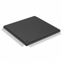


 工商网监
湘ICP备2023018690号
工商网监
湘ICP备2023018690号
