User's Guide
SLAU178 – April 2006
TSC2111EVM and TSC2111EVM-PDK
This user's guide describes the characteristics, operation, and use of the
TSC2111EVM, both by itself and as part of the TSC2111EVM-PDK. This evaluation
module (EVM) is a touch screen controller evaluation module, with auxiliary inputs and
battery and temperature measurement capabilities, and also a complete stereo audio
codec evaluation module, with several audio inputs and outputs, side tone, key click,
and effects capabilities. A complete circuit description, schematic diagram and bill of
materials are also included.
The following related documents are available through the Texas Instruments web site
at www.ti.com .
EVM-Compatible Device Data Sheets
1
2
3
4
5
Device
Literature Number
TSC2111
SLAS495
TAS1020B
SLES025
REG1117-5
SBVS001
TPS767D301/318
SLVS209
SN74LVC125A
SCAS290
SN74LVC1G125
SCES223
SN74LVC1G07
SCES296
Contents
EVM Overview ............................................................................................................... 3
Getting Started ............................................................................................................... 3
Program Description ......................................................................................................... 8
Other Board Level Connections .......................................................................................... 23
Physical Description ....................................................................................................... 27
List of Figures
1
2
3
4
5
6
7
8
9
10
11
12
13
Connecting the TSC2111EVM Board to Top of USBMODEVM Board ............................................... 6
TSC2111 EVM-PDK Software – Human Interface Tab ................................................................. 7
Human Interface Screen (Dot Mode)...................................................................................... 8
Human Interface Screen (Line Mode) ..................................................................................... 9
Data Acquisition Screen ................................................................................................... 10
Human Interface Screen With Enabled Buffer Function .............................................................. 11
Data Acquisition Screen, Reading Content Box........................................................................ 12
Configuration Screen ...................................................................................................... 13
Configuration Screen With External Reference Selection ............................................................ 14
Audio 1 Screen Default Configuration ................................................................................... 16
Audio 2 Screen at Default ................................................................................................. 17
Bass Boost Filter Screen Default Configuration ........................................................................ 18
Audio Effect Screen with Bad Data ...................................................................................... 22
Speedy33 is a trademark of Hyperception, Inc.
Microsoft Windows is a trademark of Microsoft Corporation.
SLAU178 – April 2006
Submit Documentation Feedback
TSC2111EVM and TSC2111EVM-PDK
1
�www.ti.com
14
15
16
17
18
19
20
21
22
23
Component Layout .........................................................................................................
Top PCB Layer .............................................................................................................
Power/Ground Plane 1 ....................................................................................................
Power/Ground Plane 2 ....................................................................................................
Bottom PCB Layer .........................................................................................................
Bottom Silkscreen and Solder Mask .....................................................................................
TSC2111EVM/TLV320AIC29EVM Schematic, Page 1 ...............................................................
TSC2111EVM/TLV320AIC29EVM Schematic, Page 2 ...............................................................
USB Board Schematic, Page 1 ...........................................................................................
USB Board Schematic, Page 2 ...........................................................................................
29
30
31
32
33
34
35
36
37
38
List of Tables
1
2
3
4
5
6
7
2
TSC2111EVM Board Default Configuration Settings ................................................................... 4
USBMODEVM Board Default Configuration Settings ................................................................... 5
Analog Interface Pinout .................................................................................................... 23
Analog Connectors ......................................................................................................... 24
Digital Interface Pinout..................................................................................................... 24
Power Supply Pin Out ..................................................................................................... 25
TSC2111EVM Bill of Materials ........................................................................................... 27
TSC2111EVM and TSC2111EVM-PDK
SLAU178 – April 2006
Submit Documentation Feedback
�www.ti.com
EVM Overview
1
EVM Overview
1.1
Features
•
•
Full-featured evaluation board to evaluate/test the TSC2111 functions and features
Modular design for use with a variety of DSP and microcontroller interface boards
The TSC2111EVM-PDK is a complete evaluation kit, which includes a TSC2111EVM board, a universal
serial bus (USB)-based motherboard, and the evaluation software for use with a personal computer
running Microsoft Windows™ operating systems (Win2000 or XP).
1.2
Introduction
The TSC2111 is an advanced analog interface circuit. It contains a complete 12-bit A/D resistive touch
screen converter, including driver and control circuits to measure touch pressure. The TSC2111
communicates with a host processor through a standard SPI serial interface. The TSC2111 offers two
auxiliary analog inputs and one input optimized for battery voltage measurement capable of reading
battery voltages up to 6 V, while operating with only a 2.7-V supply. It also has an on-chip temperature
sensor capable of 1°C resolution. In addition, a mono-input/stereo-output audio codec is included in the
TSC2111, and audio data is communicated to the device over an I2S bus. For more detail about the
device, refer to the TSC2111 data sheet.
The TSC2111EVM uses Texas Instruments' modular EVM form factor, allowing direct evaluation of the
TSC2111 performance and operating characteristics, and easing software development and system
prototyping. This EVM is compatible with the Texas Instruments 5-6K DSP Interface Board (SLAU104)
from Texas Instruments and additional third party boards such as the HPA449 demonstration board from
SoftBaugh, Inc. and the Speedy33™ from Hyperception, Inc.
The TSC2111EVM-PDK is a complete evaluation/demonstration kit, which includes the above stated
TSC2111 EVM and a USB-based motherboard called the USB-MODEVM Interface Board. Also, included
with TSC2111EVM-PDK is the evaluation software for use with a personal computer running Microsoft
Windows operating systems.
2
Getting Started
This chapter guides you through unpacking your EVM and setting it up so you can begin working with it
immediately.
2.1
Unpacking the EVM or EVM-PDK
When unpacking the TSC2111EVM or EVM-PDK, check the material in the box. The EVM kit includes the
following:
• TSC2111EVM board, PWB 6478196
• USBMODEVM board, PWM 6463995 (for TSC2111EVM-PDK only)
• CD-ROM, 6481572
If any of these components is missing, contact Texas Instruments for a replacement.
SLAU178 – April 2006
Submit Documentation Feedback
TSC2111EVM and TSC2111EVM-PDK
3
�www.ti.com
Getting Started
2.2
Default Configuration
The TSC2111EVM or EVM-PDK features a few simple means of configuring its operation. The default
settings of the EVM board are shown in Table 1, and the default settings of the USBMODEVM board are
shown in Table 2. When you unpack your TSC2111EVM-PDK, ensure that both boards have been initially
configured as listed in the two tables.
Table 1. TSC2111EVM Board Default Configuration Settings
Board
Identifier
Description
Default Settings
SW1
Headset (SPK1/SPK2) Output Mode Selection
Capless mode
JMP1
AGND and DGND connection Installed: Connect AGND to DGND
Installed
Removed: Disconnect AGND to DGND
JMP2
FW Boot source selection
Installed: boot from daughtercard EEPROM
Installed
Removed: boot from motherboard EEPROM
JMP3
(1)
AUX2 resistance measurement
measurement (1)
Removed
JMP4
AUX1 resistance
JMP5
+1.8VD to TSC2111 DVDD pin connection (2)
Installed
JMP6
+3.9VA to TSC2111 BVDD pin connection (2)
Installed
JMP7
+3.3VA to TSC2111 DRVDD pin connection (2)
Installed
JMP8
+3.3VA to TSC2111 AVDD1 pin
connection (2)
Installed
JMP9
+3.3VA to TSC2111 AVDD2 pin connection (2)
Installed
JMP10
IOVDD power selection
Connect 3 ~ 4
Connect 1 ~ 2: IOVDD = +5VD
Removed
Connect 3 ~ 4: IOVDD = +3.3VD
Connect 5 ~ 6: IOVDD = +1.8VD
JMP11
Reset connection
Installed: RESET from J4-GPIO2 and GPIO4
Removed
JMP12
IOVDD to TSC2111 IOVDD pin connection [2]
Installed
JMP13
MIC BIAS source selection
Connect 2 ~ 3
Removed: RESET from J4-GPIO2
Connect 1 ~ 2: from +3.3 VA
Connect 2 ~ 3: from TSC2111 MICBIAS_HND pin
JMP14
VGND mode Selection
Connect 1 ~ 2: TSC2111 VGND pin as VGND
Connect 1 ~ 2
Connect 2 ~ 3: TSC2111 VGND pin as CP_OUT–
JMP15
Differential MICIN selection
Removed: Single-ended MINCIN only
Removed
Connect 1 ~ 3: MICIN_HND and AUX2 diff
Connect 3 ~ 5: MICIN_HND and AUX1 diff
Connect 2 ~ 4: MICIN_HED and AUX2 diff
Connect 4 ~ 6: MICIN_HED and AUX1 diff
(1)
(2)
4
Refer to the note on the TSC2111 EVM schematic for the details of these jumpers.
JMP5, JMP6, JMP7, JMP8, JMP9, and JMP12 are installed by default. These jumpers can be replaced by current meters for
evaluating or testing the corresponding power consumption.
TSC2111EVM and TSC2111EVM-PDK
SLAU178 – April 2006
Submit Documentation Feedback
�www.ti.com
Getting Started
Table 2. USBMODEVM Board Default Configuration Settings
Board
Identifier
SW1
SW2
JMP1
Description
Onboard power supply enable
On/Off board control selection
+5VA and +5VD connection
Default Settings
SW1-1: +1.8VD Enable
On: Enabled
SW1-2: +3.3VD Enable
On: Enabled
SW2-1: Onboard EEPROM address bit A0
On: A0=0
SW2-2: Onboard EEPROM address bit A1
Off: A1=1
SW2-3: Onboard EEPROM address bit A2
On: A2=0
SW2-4: Onboard I2S
On: Onboard
SW2-5: Onboard MCLK
On: Onboard
SW2-6: Onboard SPI
On: Onboard
SW2-7: Onboard RESET
On: Onboard
SW2-8: External MCLK from J10 (EXT MCK)
Off: Not EXT
Installed: Connect +5VA to +5VD
Installed
Removed: Disconnect +5VA to +5VD
JMP2
AGND and DGND connection
Installed: Connect AGND to DGND
Removed
Removed: Disconnect AGND to DGND
JMP3
JMP3 Connect I2C SDA pull-up to IOVDD
Removed
JMP4
JMP4 Connect I2C SCL pull-up to IOVDD
Removed
JMP5
SPI /SS select
Connect 2 ~ 3 (FSX)
Connect 1 ~ 2: /SS from CNTL
Connect 2 ~ 3: /SS from FSX
JMP6
Board power selection
JMP7
IOVDD power selection
Connect 1 ~ 2: +5VD from USB
Connect 2 ~ 3: +5VD from U2
Connect 1 ~ 2: IOVDD +5VD
Connect 3 ~ 4: IOVDD = +3.3VD
Connect 1 ~ 2
(USB)
Connect 3 ~ 4
(+3.3VD)
Connect 5 ~ 6: IOVDD = +1.8VD
JMP8
JMP8 TAS1020B P1.3 GPIO connection
Removed
JMP9
JMP9 TAS1020B P1.2 GPIO connection
Removed
JMP10
JMP10 TAS1020B P1.1 GPIO connection
Removed
JMP11
JMP11 TAS1020B P1.0 GPIO connection
Removed
JMP12
JMP12 TAS1020B P3.5 GPIO connection
Removed
JMP13
JMP13 TAS1020B P3.4 GPIO connection
Removed
JMP14
JMP14 TAS1020B P3.3 GPIO connection
Removed
SLAU178 – April 2006
Submit Documentation Feedback
TSC2111EVM and TSC2111EVM-PDK
5
�www.ti.com
Getting Started
2.3
Connection
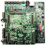
The TSC2111 EVM-PDK allows direct evaluation of the TSC2111 device with a personal computer. The
TSC2111EVM board, as the daughtercard, is installed on the top of the USBMODEVM motherboard, as
shown in Figure 1.
Use a USB cable to connect the PC to the EVM system through the J7 USB connector on the
USBMODEVM card.
Figure 1. Connecting the TSC2111EVM Board to Top of USBMODEVM Board
6
TSC2111EVM and TSC2111EVM-PDK
SLAU178 – April 2006
Submit Documentation Feedback
�www.ti.com
Getting Started
2.4
Quick Start
After the TSC2111EVM-PDK has been unpacked, and you have verified that both the daughter board
(TSC2111EVM) and the motherboard (USBMODEVM) had been configured as shown in Table 1 and
Table 2, and connected as shown in Figure 1, install the software from the included CD-ROM.
Run the Setup program on the supplied CD-ROM to install the TSC2111EVM software on your PC. Follow
the instructions provided by the installer. When the installation is complete, connect a USB cable from the
PC to J7 on the motherboard. When the TSC2111EVM-PDK is connected to the PC for the first time, the
user may see a message that a Human Interface/Audio Device has been connected. Once this connection
has been made, launch the TSC2111EVM software on the PC. The software should automatically find the
TSC2111EVM. If the board is found, the screen shown in Figure 2 appears.
Figure 2. TSC2111 EVM-PDK Software – Human Interface Tab
To use the touch screen features, a 4-wire resistive touch screen can be connected to J1A or J6 on the
TSC2111EVM daughter board. Note the correct X+(J1A-2), X-(J1A-4), Y+(J1A-6) and Y-(J1A-8) locations
when connecting.
With the firmware/software default configuration, the TSC2111 audio output OUT8 is powered up, and the
side tone and the key click functions are activated. To verify the functionality of the EVM system, a
speaker (8-ohms or above) can be connected to J13 (the loudspeaker connection terminal or OUT8) on
the TSC2111EVM daughter-card. A 'ding' sound should be heard when the USB cable from the PC is
plugged into the motherboard (J7). Additional dings are heard when launching the software. Sounds
picked up by the onboard microphone (MK1) on the daughter board should be able be audible through the
speaker.
SLAU178 – April 2006
Submit Documentation Feedback
TSC2111EVM and TSC2111EVM-PDK
7
�www.ti.com
Program Description
3
Program Description
After installing the software for the TSC2111EVM as previously described, the user can begin to evaluate
the functions of the TSC2111 using the evaluation-software graphic user interface (GUI).
The program’s interface is a simple, six-tab interface. Clicking on a tab takes you to the functions
associated with that tab. The program begins on the Human Interface screen (the default) as shown in
Figure 2.
3.1
Human Interface Screen
The Human Interface screen displays the activity on the touch screen connected to the TSC2111EVM.
The status bar at the bottom of the screen is divided into four sections showing the communication status
between the PC and the EVM-PDK. Starting from the left, the first section shows the status of the
connection. If a communication error occurs, an error message appears here; otherwise, it displays
Connected, as shown in the above Figure 2. The final section, on the right side of the status bar, shows
the number of readings per second being taken from the touch screen.
The touch screen box on this screen is updated when a touch is detected on the touch screen. As the
touch screen is drawn on, the motion on the touch screen is translated into pixels on the screen. The
software takes X and Y, or X, Y, and Z readings, which are shown numerically above this box. Even
though TSC2111 has five different touch-screen scan modes, this EVM allows only two selections at this
tab, either X and Y, or X, Y, and Z. Default is the X, Y, and Z mode. In X and Y mode, the pixel size is
fixed. In the X, Y, and Z mode, as the touch pressure is increased, the pixel size increases. A lighter touch
results in smaller pixel sizes. Refer to Figure 3.
Figure 3. Human Interface Screen (Dot Mode)
8
TSC2111EVM and TSC2111EVM-PDK
SLAU178 – April 2006
Submit Documentation Feedback
�www.ti.com
Program Description
The X and Y, or X, Y, and Z mode is selected by clicking on the option at the A/D Mode Selection Box.
The touch action is shown on the screen in dot mode, as shown in Figure 3, or solid line mode as shown
in Figure 4. The dot line mode is selected by the corresponding option above the drawing screen.
Figure 4. Human Interface Screen (Line Mode)
The display can be cleared by pressing Enter on the PC keyboard.
The window to the right of the screen shows the touch screen data when the TSC2111 is in buffer mode.
For the details on the buffer mode, refer to the TSC2111 datasheet and the next section Data Acquisition
Screen.
SLAU178 – April 2006
Submit Documentation Feedback
TSC2111EVM and TSC2111EVM-PDK
9
�www.ti.com
Program Description
3.2
Data Acquisition Screen
Clicking on the Data Acquisition tab brings up the screen as shown in Figure 5.
Figure 5. Data Acquisition Screen
3.2.1
Nontouch Data Acquisition
At this screen, while the Buffer Mode is not enabled, the TSC2111 samples the battery and auxiliary input
voltage readings, and then the TEMP1 and TEMP2 measurements. These measurements are all repeated
twice per second, and the results are displayed on the three boxes at the left side of this screen.
10
TSC2111EVM and TSC2111EVM-PDK
SLAU178 – April 2006
Submit Documentation Feedback
�www.ti.com
Program Description
3.2.2
Buffer Function
In the middle of the screen are the Buffer Mode settings. By default, the buffer function is disabled, and all
touch or non-touch data are converted and stored to the corresponding registers. When the buffer function
is enabled by checking the Enable option, the data is converted and saved to the buffer registers in Page
3 of the TSC2111 memory space. Refer to the data sheet for the details of the buffer function.
Below the Buffer Trigger slider, the Read Buffer for Touch Screen Data button can be used to place the
TSC2111 into self-controlled mode, and the Read Buffer for Non Touch Screen Data button can be used
to select host-controlled mode.
When the Read Buffer for Touch Screen Data button is clicked, the interface switches from this screen to
the Human Interface screen. The touch-screen data in the TSC2111 page 3 registers is displayed in the
Buffer Contents box when the screen is touched, as Figure 6 illustrates. Note that in buffer mode, the
touch screen data does not show up on the touch screen drawing box. In XY A/D mode, the data list is in
the sequence of X, Y, X, Y, X, Y, etc. And under the XYZ A/D mode, the data is that of X, Y, Z1, Z2, X, Y,
Z1, Z2, X, etc.
Figure 6. Human Interface Screen With Enabled Buffer Function
Clicking on the Read Buffer for Non Touch Screen Data button places the TSC2111 in auto-scan mode.
This automatically scans the AUX1, AUX2, and TEMP1 inputs, and displays nontouch screen raw data in
the Reading Content box on the right side of the display under the Data Acquisition tab, as shown in
Figure 7. The data in the Reading Content box shown in Figure 7 is listed in this order: AUX1, AUX2,
TEMP1, AUX1, AUX2, TEMP1, AUX1, etc.
SLAU178 – April 2006
Submit Documentation Feedback
TSC2111EVM and TSC2111EVM-PDK
11
�www.ti.com
Program Description
Figure 7. Data Acquisition Screen, Reading Content Box
The Buffer Trigger level slider can be set to either 8 or 16. Even though the TSC2111 can be set to a
higher trigger level up to 64, this EVM allows only 8 or 16. The buffer function can be controlled in either
Continuous or Single Shot mode, which is selected on the mode-control option box. Refer to the data
sheet for more on the TSC2111 buffer function.
The data in the list is cleared by clicking on the Clear List button on this screen
3.2.3
Displaying Register Contents
Five additional register-read buttons access the corresponding registers, and move the raw data into the
list. This is helpful for testing and debugging.
12
TSC2111EVM and TSC2111EVM-PDK
SLAU178 – April 2006
Submit Documentation Feedback
�www.ti.com
Program Description
3.3
Configuration Screen
This screen accesses all the configurable settings for the TSC2111 analog-to-digital converter (ADC) and
reference as shown in Figure 8.
Figure 8. Configuration Screen
3.3.1
ADC Control Section
The ADC Control box has a check box to disable the Pen Touch Detection function of TSC2111. See the
TSC2111 Data Sheet for information about this function.
The sliders in this section control the parameters of the ADC, for the touch (XYZ) and non-touch (BAT,
AUX1, AUX2, TEMP1, TEMP2) data. Each slider controls one parameter, whose value is shown next to
the slider.
• Resolution — Selects between 8–, 10–, and 12–bit resolution.
• Conversion Clock — The internal clock that runs the ADC can run at 8, 4, 2, or 1 MHz. When running
at 8 MHz, only 8-bit resolution is possible; when running at 4 MHz, only 8- or 10-bit resolution is
possible. Only 1- or 2-MHz clock rates allow 12-bit resolution to be chosen.
• Panel Voltage Stabilization Time — This is the time that the TSC2111 allows for the touch screen to
stabilize after turning the drivers on.
• Precharge Time and Sense Time — These two parameters are the time allowed to precharge the
touch panel capacitance, and then sense to see if the screen is touched. For more details on these
parameters, refer to the TSC2111 data sheet.
• Average/Median — There are two ways to reduce noise effects on the ADC measurements. One is
averaging, where 4, 8, or 16 readings are averaged; another option is to find the median value among
5, 9, or 15 readings. The default is the average mode, as shown in Figure 8. Median mode can be
selected with the corresponding button.
SLAU178 – April 2006
Submit Documentation Feedback
TSC2111EVM and TSC2111EVM-PDK
13
�www.ti.com
Program Description
Note that these settings apply to all operations of the A/D converter, not just the touch screen operations.
Thus, resolution and averaging can be changed to increase accuracy in the data acquisition functions.
3.3.2
Reference Section
The touch screen function is always performed using a ratiometric or differential mode on this EVM set to
obtain better touch readings. For all other A/D functions (non-touch measurements such as BAT), a
reference voltage is needed for the A/D converter. Figure 8 shows this section with the TSC2111 internal
reference chosen.
The internal reference voltage can be set to either 1.25 V or 2.5 V. The internal reference powers down
between conversions to save power. The Powered at all times checkbox overrides this feature, and the
reference does not power down. If the reference is allowed to power down, the TSC2111 must allow a
delay time for the reference to power up when a conversion is to take place. This delay time can be set
using the slider in this section.
If an external reference is to be used, it can be selected as shown in Figure 9. The value of the external
reference should be entered in the text box shown.
Figure 9. Configuration Screen With External Reference Selection
14
TSC2111EVM and TSC2111EVM-PDK
SLAU178 – April 2006
Submit Documentation Feedback
�www.ti.com
Program Description
3.3.3
Measurement Section
The TSC2111 supports programmable, automatic temperature and auxiliary-input measurements. In the
auto measurement mode, the TSC2111 can auto start the TEMP1, TEMP2, AUX1, and/or AUX2
measurement after a programmable interval. The checkboxes and sliders in the Measurement section
provide choices.
Additionally, the AUX1 and AUX2 can be configured to measure voltage or resistance. Under the
resistance measurement, the bias can be configured as external or internal by checking or unchecking the
Enable External Bias Resistance box.
3.3.4
Threshold Section
The TSC2111 monitor the temperature and the auxiliary inputs and set corresponding flags if an input
exceeds the bounds set in the threshold registers.
In this section, if the threshold function has not been enabled (Enable checkbox has not been checked),
the corresponding MAX/MIN slider does not move. Also note that the MAX value must be greater than or
equal to the MIN value.
3.3.5
Continuous Conversion Delay Section
In auto-measurement mode, the delays between the conversions are programmable. This section can be
used to program to delays between the continuous conversions.
The nontouch and touch auto measurement delays can be programmed individually. By clicking on the
corresponding Enable checkbox, the auto-measurement delay is enabled. The delay-time option allows
selection of delay-clock source and divider.
The clock used can be the internal oscillator or the external MCLK. The clock divider (CLKDIV) is used to
derive the 1-MHz clock for the programmable delay. This sets the CLKDIV so that MCLK/CLKDIV = 1
MHz.
3.3.6
Reinitialization and Reset
Two buttons on this screen allow the user to reset and reinitialize the TSC2111.
By clicking the SW Reset button, a software device reset is issued to the TSC2111. By clicking the Init
TSC2111 button, the control registers (for ADC and audio) revert back to the startup (firmware) default
settings.
To restore the TSC2111 EVM to its power-up state, click SW Reset, followed by Init TSC2111.
SLAU178 – April 2006
Submit Documentation Feedback
TSC2111EVM and TSC2111EVM-PDK
15
�www.ti.com
Program Description
3.4
Audio Screens
Three tabs control the TSC2111 audio functions: Audio 1, Audio 2, and Audio Effects Filters tabs.
Figure 10 shows the default configuration of the Audio 1 tab with the following sections:
• INTERFACE: Audio I2S port
• PLL: PLL parameters, FSref frequency
• ADC: Audio ADC, ADC input source selection
• DAC/Outputs: Audio DAC, other analog-output features
• GPIO1: GPIO1 function/status
• GPIO2: GPIO2 function/status
Figure 10. Audio 1 Screen Default Configuration
16
TSC2111EVM and TSC2111EVM-PDK
SLAU178 – April 2006
Submit Documentation Feedback
�www.ti.com
Program Description
Figure 11 shows the default condition of the Audio 2 tab. The functions and setting on Audio 2 primarily
control the audio analog inputs with the following sections:
• HeadSet: Headset input power and gain control (PGA or AGC) function and other headset specified
functions.
• HandSet: Handset input power and gain control (PGA or AGC) function and other handset specified
functions.
• Cell Phone: Cell-phone input power and gain control (PGA or AGC) function.
• SideTone: Sidetone power and gain.
• KeyClick: Key-click tone.
• Buzz Input: Power and gain for the BUZZ_IN input pin.
Figure 11. Audio 2 Screen at Default
SLAU178 – April 2006
Submit Documentation Feedback
TSC2111EVM and TSC2111EVM-PDK
17
�www.ti.com
Program Description
Figure 12 shows the default configuration of the AudioEffects Filters tab. This tab displays the boost filters,
the de-emphasis filter, and the DAC and output driver pop-noise reduction functions.
Figure 12. Bass Boost Filter Screen Default Configuration
3.4.1
Interface Section
This section (refer to Figure 10) controls the behavior of the I2S port (BCLK, LRCLK, DIN, and DOUT
pins). In this EVM, the audio port transfers 16-bit data in I2S format, and the codec reference sample rate
is 44.1 kHz.
The TSC2111 is programmed as an I2S slave by default. The onboard processor TAS1020B is the master,
which generates the BCLK and LRCLK signal. If the TSC2111 is used as a master, the onboard processor
should be disabled and the I2S port should be detached from the processor by turning off the onboard I2S
interface. Refer to Table 2 in the Default Configurations 2.2 section.
18
TSC2111EVM and TSC2111EVM-PDK
SLAU178 – April 2006
Submit Documentation Feedback
�www.ti.com
Program Description
3.4.2
PLL Section
There is an on-chip phase-locked loop (PLL) in the TSC2111. The PLL can be enabled or disabled, based
on the given master clock (MCLK) to the TSC2111 and the required reference frequency (FSref) for the
codec. For more details on the PLL, refer to the TSC2111 data sheet.
The PLL can be set on the PLL Secton of Audio 1 screen (Figure 10).
The default frequencies for this EVM board are
• MCLK = 11.2896 MHz
• Reference sample rate = 44.1 kHz
At the bottom of the section, the corresponding FSref frequency is shown based on the selection of:
1. the Q-value if the PLL has not been enabled, or
2. the P, J, D values if the PLL has been enabled.
3.4.3
ADC Section
This section (Audio 1 Tab, Figure 10) configures the audio ADC power and the analog input source.
By default, the audio ADC is powered up so that the audio-recording function can start running with the
default settings. Checking Power Down ADC disables the audio ADC.
The ADC sample rate can be set as a divider frequency from the reference frequency, FSref. For
example, when FSref = 44.1 kHz (set in the INTERFACE section of the same tab), an 8-K sample rate is
obtained by setting the divider to 5.5 (44100/5.5 = 8018 Hz).
The audio ADC also has a high-pass filter, which is a sub-multiple of the sample rate, to remove dc or low
frequency components from the input signal.
The input signal to the audio ADC can be selected from different analog resources under different modes
using the Select ADC Input Source option list. The microphone input from the headset or the handset can
be selected; the single-ended or the differential input (paired with AUX1 or AUX2) can be used.
The cell-phone input can also be connected to the audio ADC.
3.4.4
DAC/Outputs Section
This section configures the audio DAC power and all functions of the analog outputs, such as power, gain,
mode, and destination, which identifies the analog output pin or pins where the analog output signal is
sent.
In the Power Down subsection, the DAC and the output driver circuits can be powered up/down
individually. By checking a checkbox, the corresponding TSC2111 circuit is powered down.
In the SC Protect subsection, the short-circuit (SC) protection function can be enabled or disabled. When
the short-circuit protection function is enabled and a short-circuit occurs, all analog outputs are disabled
and the corresponding flag is set. For example, to set the headset SC protection, check the box. In the
event of a headset short circuit, all analog outputs are disabled, and D1 of control registers in page 2
address 0x1D is set. The TSC2111 requires hardware or software reset to return to normal operation.
Similar to the ADC, the DAC sample rate can be set as a divider frequency from the reference FSref
frequency, through the DAC Sample Rate option list.
The TSC2111 has the capability to route the stereo DAC output signals to the selected analog output. To
route the signals to the headset drivers (SP1 and SP2 pins), select from the DAC Output to lists. By
default, the left channel DAC output is routed to SP1 and the right channel to SP2.
The signal routed to SP1 can also be output to the loud speaker (OUT8P/OUT8N), if the SP1 to Loud SP
checkbox is checked.
The SP1 output can be used in single-ended or differential mode. In single-ended mode, it is driven as
one channel of the stereo headset outputs, and the audio sound is output through a headset at J11 on the
TSC2111EVM daughtercard. In differential mode, the SP1 is paired with the OUT32N pin as the receiver
driver, and the audio sound is output through a speaker connected to the terminal block J2 on the
TSC2111EVM. By default, the SP1 is set to single-ended mode.
SLAU178 – April 2006
Submit Documentation Feedback
TSC2111EVM and TSC2111EVM-PDK
19
�www.ti.com
Program Description
Other signals, such as the SideTone, KeyClick, CP_IN, and BUZZ_IN can be routed to speaker 1 (SP1),
speaker 2 (SP2), and/or the loud speaker (LoudSP). Signal selection can be done in this section by
checking the corresponding checkbox.
The signals to SP1, SP2, or the ADC can be output to the TSC’s cellphone output pin, and the BUZZ_IN,
SP1 and SP2 signals can also be output the BUZZ_IN PGA.
The DAC PGA gain can be set to soft-stepping mode. In soft-step mode, the soft stepping can be set to
either 0.5–dB per one sample, or 0.5–dB per two samples.
The stereo DAC audio volume is controlled by the left (L) and right ®) volume control slides, selectable
through setting the master volume controller, in three different ways:
• Independent,
• Right channel controlled, or
• Left channel controlled.
In addition to the left and right DAC channel volume controls and mutes, the analog signals from the
SPK1, SPK2, OUT8P/OUT8N (loud speaker), and CP_OUT pins can be individually muted or unmuted.
The TSC2111 supports both capacitor-coupled (cap) and capacitorless (capless) headset interfaces
through settings in software and hardware. To use the capless outputs, Check the box Enable Capless
Headset Output, and select the CAPLESS setting on SW1 on the TSC2111EVM daughter board.
Note:
3.4.5
The settings of SW1 and Enable Capless Headset Output must match for proper EVM
operation.
GPIO1 and GPIO2 Sections
The two GPIO pins on the TSC2111 are programmed for several different functions, selectable through
the GPIO1 or GPIO2 section. Refer to the data sheet for all of the functions. When a GPIO pin is used as
a digital output, its status can be controlled by the GPO Command to either logic high or low. When not
being used, the GPIO pin should be set to high impedance (Hi-Z).
3.4.6
Headset Section
The headset configuration section is in the Audio 2 tab, which is used mainly to set the headset input gain
through the headset PGA or the AGC, selectable by the Headset/AUX Input AGC ON checkbox.
By default, the AGC is OFF, and the programmable-gain amplifier (PGA) on the headset circuit is selected
for the gain control, allowing analog-input gain control from 0 dB to 59.5 dB. When the AGC is OFF,
moving the volume slide on the AGC OFF subsection adjusts the PGA on the MICIN_HED path. Checking
the Mute box mutes the headset input signal.
When the PGA changes from the current value to a newly programmed value, the change rate can be
controlled if the PGA Soft Stepping box is checked in the Head/Handset MIC PGA section, where the PGA
changes 0.5 dB at either 1 step per sample or one step per two samples.
When the box by AGC ON is checked, the AGC is enabled. Refer to the TSC2111 data sheet and the
appreciated application note(s) for setting and using the AGC.
In addition to the input-gain control, the headset microphone bias can be selected. The programmable
de-bounce features for the headset and button detect are also configured in this section. Refer to the data
sheet for the details on detection and de-bounce.
20
TSC2111EVM and TSC2111EVM-PDK
SLAU178 – April 2006
Submit Documentation Feedback
�www.ti.com
Program Description
3.4.7
Handset Section
Similar to the headset section, the handset section is used mainly to configure the handset input gain
through the handset PGA or the AGC, selectable by the Handset Input AGC ON checkbox.
By default, when the handset AGC is OFF, and the programmable gain amplifier (PGA) is selected for the
input gain control, allowing analog input gain control from 0 dB to 59.5 dB. When the AGC is off, moving
the volume slide on the AGC OFF subsection adjusts the PGA on the MICIN_HND path. Checking the
Mute box mutes the handset input signal.
The handset and headset share the soft-stepping settings. Refer to the explanation in the Headset Section
for the feature and settings.
Similar to the headset, when the box by AGC ON is checked, the handset AGC is enabled.
In addition to the handset input-gain control, the handset microphone bias can be selected in the Handset
Section, similar to that in the Headset Section.
3.4.8
Cell-Phone Section
The Cell-Phone section is used to configure the cell-phone input gain, by using the CP_IN PGA or AGC.
When the checkbox by Cell Phone Input AGC ON, is not checked, the PGA controls the gain, from –34.5
dB to 12 dB, and in 0.5 dB steps if the soft-stepping option is selected. The cell-phone input is muted
when the Mute box under the slider is checked.
When the box by AGC ON is checked, the cell-phone input AGC is enabled. Refer to the TSC2111 data
sheet or the appropriate application report(s) for setting and using the AGC.
At the TSC2111, both CP_IN and CP_OUT signals can be at single-ended or differential mode. The
corresponding software settings can be found in this section.
3.4.9
Sidetone Section
The TSC2111 has an analog sidetone circuit. The audio outputs of the TSC2111 includes a mixer so that
the sidetone can be mixed with the audio output signals, in proportion to their respective volume settings.
The sidetone is enabled when the PowerUp box is checked. Its volume can be adjusted by the analog
volume control slider, ranging from –34.5 dB to12 dB, and in 0.5-dB steps if the soft-stepping option is
used. The sidetone is muted when the Mute box under the slider is checked.
At the EVM power up, the sidetone is defaulted to power up.
3.4.10
Keyclick Section
When the Enable Key Click box is checked, a clicking sound is heard whenever an audio-related setting is
selected or checked in the Audio 1, Audio 2 and the Audio Effects Filters screens.
The volume, frequency, and duration (length) of this keyclick can be adjusted using the corresponding
slider and selectors.
At the EVM power up, the keyclick is enabled by default.
3.4.11
Buzz Input Section
The buzzer input from the cell phone can be routed to the TSC2111 through the BUZZ_IN pin, if the
checkbox by PowerDown is not selected. This input path supports the PGA range of from –45 dB to 0 dB,
in 3 dB steps if the soft-stepping option was chosen.
SLAU178 – April 2006
Submit Documentation Feedback
TSC2111EVM and TSC2111EVM-PDK
21
�www.ti.com
Program Description
3.4.12
Audio Effects
The programmable Audio Effects filters coefficients of the TSC2111 can be accessed in the Audio Effect
Filters screen, as shown in Figure 12.
Different filter coefficients can be loaded for left and right channels, although these are typically set to the
same values.
If changes are made directly to coefficient values, the response can be viewed on the graph by clicking
the View Response button. It is recommended that the user view the response before downloading values
to the TSC2111, as some values can cause clipping or oscillation of the filter. The filter equation is
described in the TSC2111 data sheet. When the data entered is outside the acceptable range, a warning
window appears to indicate the improper coefficient, as shown in Figure 13.
Figure 13. Audio Effect Screen with Bad Data
In addition to the direct coefficient settings previously described, there are six preconfigured filters
designed with the EVM software, selectable using the drop-down list of this screen. When a preconfigured
filter is selected, the coefficients are updated along with the graph of the filter response to the selection.
However, nothing is loaded into the TSC2111 until the Download button is clicked. Checking the Boost
Filter box enables the filter selected.
3.4.13
Deemphasis Filter
In addition to the boost filter, a de-emphasis filter is provided by the TSC2111 for the audio DAC.
Checking the Deemphasis Filter On box enables the filter.
22
TSC2111EVM and TSC2111EVM-PDK
SLAU178 – April 2006
Submit Documentation Feedback
�www.ti.com
Other Board Level Connections
3.4.14
Power-Up Pop Reductions
Settings on this tab can reduce the pop noise heard at the moment the TSC2111 output circuit is powered
up. The pop noise reduction can be set on the DAC or the analog output driver circuit. Click on the Enable
DAC HP PR checkbox to enable the DAC pop-reduction feature, and the Enable Driver PR checkbox to
enable the output driver pop-reduction feature. Change the Driver PR Duration to set and optimize the
noise reduction effects.
4
Other Board Level Connections
This chapter describes the board-level connectors of the TSC2111EVM or EVM-PDK. Using these
connectors, the TSC2111 EVM can operate as a stand-alone unit, or as the daughter-board of the
USBMODEVM.
4.1
Analog Interface
For maximum flexibility, the TSC2111EVM is designed for easy interface to multiple analog sources.
Samtec part numbers SSW-110-22-F-D-VS-K and TSM-110-01-T-DV-P provide a convenient 2x10-pin
dual-row header/socket combination at J1 and J2. These headers/sockets provide access to the analog
input and output pins of the device. Table 3 summarizes the analog interface pinout for the TSC2111EVM.
Table 3. Analog Interface Pinout
Pin Number
Signal
Description
J1.1
CP_IN+
Input from cell-phone module (+)
J1.2
X+
Touch screen X+ position input and driver
J1.3
CP_IN–
Input from cell-phone module (-)
J1.4
X–
Touch screen X– position input and driver
J1.5
CP_OUT+
Output to cell-phone module (+)
J1.6
Y+
Touch screen Y+ position input and driver
J1.7
CP_OUT–
Output to cell-phone module (-)
J1.8
Y–
Touch screen Y– position input and driver
J1.9
AGND
Analog ground
J1.10
VBAT
Battery monitor input
J1.11
AGND
Analog ground
J1.12
AUX1
First auxiliary input
J1.13
AGND
Analog ground
J1.14
NC
Not connected
J1.15
NC
Not connected
J1.16
AUX2
Second auxiliary input
J1.17
AGND
Analog ground
J1.18
AGND
Analog ground
J1.19
AGND
Analog ground
J1.20
REF+
Reference Voltage
J2.1
OUT32N
Receiver driver output (–)
J2.2
SPK1
Headset driver output (1) /receiver driver output (+)
J2.3
VGND
Virtual ground for audio outputs
J2.4
SPK2
Headset driver output (2)
J2.5
OUT8N
Loudspeaker driver output (–)
J2.6
OUT8P
Loudspeaker driver output (+)
J2.7
MICBIAS_HED
Headset microphone bias voltage
J2.8
MICIN_HED
Headset microphone input
J2.9
AGND
Analog ground
SLAU178 – April 2006
Submit Documentation Feedback
TSC2111EVM and TSC2111EVM-PDK
23
�www.ti.com
Other Board Level Connections
Table 3. Analog Interface Pinout (continued)
Pin Number
Signal
Description
J2.10
MIC_DETECT_IN
Microphone detect input
J2.11
AGND
Analog ground
J2.12
SPKFC
Driver feedback/speaker detect input
J2.13
AGND
Analog ground
J2.14
MICIN_HND
Handset microphone input
J2.15
NC
Not connected
J2.16
MICBIAS_HND
Handset microphone bias voltage
J2.17
AGND
Analog ground
J2.18
NC
Not connected
J2.19
AGND
Analog ground
J2.20
NC
Not connected
In addition to the J1-J2 analog headers, the analog inputs and outputs may also be accessed through
alternate connectors, either screw terminals or audio jacks, listed in Table 4.
Table 4. Analog Connectors
4.2
Description
Pin1
Pin2
Pin3
Pin4
J6
J6 Touch Screen
X–
Y+
X+
Y–
Pin5
—
J7
J7 External Inputs
VBAT
AUX1
AUX2
AGND
—
J9
J9 Cell-phone In/Out
CP_IN/CP_IN+
BZ_IN/CP_IN–
CP_OUT+
CP_OUT–
AGND
J10
J10 External MIC Input
MICIN_HND
Onboard MIC
Onboard MIC
MICBIAS_HND
AGND
J11
J11 Headset
MICIN_HED
SPK2
SPK1
VGND/GND
J12
J12 Receiver (OUT32)
OUT32N
OUT32P
—
—
—
J13
J13 Loud-speaker (OUT8)
OUT8N
OUT8P
—
—
—
—
Digital Interface
The TSC2111EVM is designed to easily interface with multiple control platforms. Samtec part numbers
SSW-110-22-F-D-VS-K and TSM-110-01-T-DV-P provide a convenient 2x10-pin dual-row header/socket
combination at J4 and J5. These headers/sockets provide access to the digital control and serial data pins
of the device. Table 5 summarizes the digital interface pinout for the TSC2111EVM.
Table 5. Digital Interface Pinout
Pin
Number
24
Signal
Description
J4.1
NC
Not Connected
J4.2
GPIO1
General purpose I/O 1
J4.3
SCLK
SPI Interface serial clock input
J4.4
DGND
Digital ground
J4.5
NC
Not Connected
J4.6
GPIO2
General purpose I/O 2
J4.7
SS
SPI Interface slave select input
J4.8
RESET
Selectable to TSC2111 reset
J4.9
NC
Not Connected
J4.10
DGND
Digital ground
J4.11
MOSI
SPI serial data mater-OUT-slave-IN
J4.12
NC
Not Connected
J4.13
MISO
SPI serial data mater-IN-slave-OUT
TSC2111EVM and TSC2111EVM-PDK
SLAU178 – April 2006
Submit Documentation Feedback
�www.ti.com
Other Board Level Connections
Table 5. Digital Interface Pinout (continued)
Pin
Number
4.3
Signal
Description
J4.14
RESET
TSC2111 reset
J4.15
PINTDAV
Pen-interrupt/data-available output
J4.16
SCL
I2C interface clock line
J4.17
NC
Not Connected
J4.18
DGND
Digital ground
J4.19
PWR_DN
Hardware power down input
J4.20
SDA
I2C interface data line
J5.1
NC
Not Connected
J5.2
NC
Not Connected
J5.3
BCLK
I2S interface audio bit clock
J5.4
DGND
Digital ground
J5.5
NC
Not Connected
J5.6
NC
Not Connected
J5.7
WCLK
I2S interface audio word clock
J5.8
NC
Not Connected
J5.9
NC
Not Connected
J5.10
DGND
Digital ground
J5.11
DIN
I2S interface data input
J5.12
NC
Not Connected
J5.13
DOUT
I2S interface data output
J5.14
NC
Not Connected
J5.15
NC
Not Connected
J5.16
SCL
I2C interface clock line
J5.17
MCLK
Master clock
J5.18
DGND
Digital ground
J5.19
NC
Not Connected
J5.20
SDA
I2C interface data line
Power Supplies
J3 provides power to the EVM on the pins listed in Table 6.
Table 6. Power Supply Pin Out
Signal
Pin Number
Signal
NC
J3.1
J3.2
+5VA
J3.3
J3.4
NC
NC
DGND
J3.5
J3.6
AGND
+1.8VD
J3.7
J3.8
NC
+3.3VD
J3.9
J3.10
+5VD
The TSC2111EVM-PDK motherboard (the USB-MODEVM Interface board) supplies power to J3 of the
TSC2111EVM. Power for the motherboard is supplied either through its USB connection or via terminal
blocks on that board.
SLAU178 – April 2006
Submit Documentation Feedback
TSC2111EVM and TSC2111EVM-PDK
25
�www.ti.com
Other Board Level Connections
4.3.1
Stand-Alone Operation
When used as a stand-alone EVM, power can be applied to J3 directly. The user must reference the
supplies to the appropriate grounds on that connector.
CAUTION
Verify that all power supplies are within the safe operating limits shown on the
TSC2111 data sheet before applying power to the EVM.
4.3.2
USB-MODEVM Interface Power
The USB-MODEVM Interface board can be powered from several different sources:
• USB
• 6 V - 10 V dc external AC wall supply (not included)
• Lab power supply
When powered from the USB connection, JMP6 must have a shunt from pins 1–2 (this is the default
factory configuration). When powered from 6 V - 10 V dc, either through the J8 terminal block or the J9
barrel jack, JMP6 must have a shunt installed on pins 2-3. If power is applied in any of these ways,
onboard regulators provide the required supply voltages; no other power supplies are necessary.
If lab supplies are used to provide the individual voltages required by the USB-MODEVM Interface, JMP6
must have no shunt installed. Voltages are then applied to J2 (+5VA), J3 (+5VD), J4 (+1.8VD), and J5
(+3.3VD).
The +1.8VD and +3.3VD can also be generated on the board by the onboard regulators from the +5VD
supply. To enable this configuration, the switches on SW1 must be set to enable the regulators by placing
them in the ON position (lower position, looking at the board with text reading right-side up). If +1.8VD and
+3.3VD are supplied externally, disable the onboard regulators by placing SW1 switches in the OFF
position.
Each power supply voltage has an LED (D1-D7) that illuminates when the power supply is active.
4.4
External Voltage Reference
If the external voltage reference is used, the reference can be input to the TSC2111 device through the J8
terminal block.
26
TSC2111EVM and TSC2111EVM-PDK
SLAU178 – April 2006
Submit Documentation Feedback
�www.ti.com
Physical Description
5
Physical Description
This chapter contains the bill of materials, the TSC2111 EVM board layout, and the schematics.
5.1
Bill of Materials
Table 7. TSC2111EVM Bill of Materials
Item
Qty
Value
Ref. Des.
Description
Manufacturer
Part Number
1
6
0Ω
R9-R14
1/8W 5% Chip Resistor
Panasonic
ERJ-6GEY0R00V
2
1
0Ω
R25, R27
1/4W 5% Chip Resistor
Panasonic
ERJ-8GEY0R00V
3
1
220 Ω
R15
1/8W 5% Chip Resistor
Panasonic
ERJ-6GEYJ221V
4
1
2.2 KΩ
R26
1/4W 5% Chip Resistor
Panasonic
ERJ-8GEYJ222V
5
3
2.7 KΩ
R7, R28, R29
1/10W 5% Chip Resistor
Panasonic
ERJ-3GEYJ272V
6
1
2.7 KΩ
R8
1/4W 5% Chip Resistor
Panasonic
ERJ-8GEYJ272V
7
1
30.1 KΩ
R6
1/16W 1% Chip Resistor
Panasonic
ERJ-3EKF3012V
8
1
69.8 KΩ
R5
1/16W 1% Chip Resistor
Panasonic
ERJ-3EKF6982V
9
4
100 KΩ
R1, R2, R3, R4
1/10W 5% Chip Resistor
Panasonic
ERJ-3GEYJ104V
Not
9
Installed
NI
R16-R24
10
0.1 µF
C7-C9, C11-C19
25V Ceramic Chip Capacitor, +/ 10%, X7R
TDK
C1608X7R1E104KT
Not
7
Installed
0.1 µF
C20-C26
25V Ceramic Chip Capacitor, +/ 10%, X7R
TDK
C2012X7R1E104KT
11
2
0.1 µF
C10, C35
100V Ceramic Chip Capacitor, +/ 10%, X7R
TDK
C3216X7R2A104KT
12
1
0.33 µF
C1
10V Ceramic Chip Capacitor, +/ 10%, X5R
TDK
C1608X5R1A334KT
13
10
10 µF
C2-C6, C27-C31
6.3V Ceramic Chip Capacitor, +/ 10%, X5R
TDK
C3216X5R0J106KT
14
2
47 µF
C36, C37
6.3V Ceramic Chip Capacitor, +/ 20%, X5R
TDK
C3225X5R0J476MT
NI
C32, C33, C34
12
Not
3
Installed
15
1
U3
Touch Screen Controller, Audio
Codec
Texas Instruments
TSC2111IRGZG4
16
1
U2
64K, I2C EEPROM
Microchip
24AA64-I/SN
17
1
U1
Dual Output LDO Voltage
Regulator
Texas Instruments
TPS767D301PWPG4
18
2
J6, J7
Screw Terminal Block, 4 Position
On Shore
Technology
ED555/4DS
19
1
J9
Screw Terminal Block, 5 Position
On Shore
Technology
ED555/5DS
20
3
J8, J12, J13
Screw Terminal Block, 2 Position
On Shore
Technology
ED555/2DS
21
1
J10
3.5mm Audio Jack, T-R-S, SMD
CUI Inc.
SJ1-3515-SMT
22
1
J11
3.5mm Audio Jack, T-R-S-G,
Thru-Hole
CUI Inc.
SJ-43514
23
4
J1A, J2A, J4A, J5A 20 Pin SMT Plug
Samtec
TSM-110-01-L-DV-P
24
4
J1B, J2B, J4B, J5B 20 pin SMT Socket
Samtec
SSW-110-22-F-D-VS-K
25
1
J3A
10 Pin SMT Plug
Samtec
TSM-105-01-L-DV-P
26
1
J3B
10 pin SMT Socket
Samtec
SSW-105-22-F-D-VS-K
27
1
N/A
TSC2111EVM PWB (must be
RoHS compliant)
Texas Instruments
6478197
D1, D2, D3, D4
Schottky Barrier Diode, Series
Configuration
Diodes Inc.
BAT54S-7-F
Not
4
Installed
NI
SLAU178 – April 2006
Submit Documentation Feedback
TSC2111EVM and TSC2111EVM-PDK
27
�www.ti.com
Physical Description
Table 7. TSC2111EVM Bill of Materials (continued)
28
Item
Qty
Ref. Des.
Description
Manufacturer
Part Number
28
3
Value
JMP1, JMP2,
JMP11
2 Position Jumper , 0 .1" spacing
Samtec
TSW-102-07-L-S
Not
2
Installed
JMP3, JMP4
2 Position Jumper , 0 .1" spacing
Samtec
TSW-102-07-L-S
29
2
JMP13, JMP14
3 Position Jumper , 0 .1" spacing
Samtec
TSW-103-07-L-S
30
2
JMP10, JMP15
3 X 2 Position Header, 0 .1"
spacing
Samtec
TSW-103-07-L-D
31
6
JMP5-JMP9,
JMP12
Bus Wire, 18-22 Gauge
32
1
MK1
Omnidirectional Microphone
Cartridge
Knowles Acoustics
MD9745APZ-F
33
1
SW1
4PDT Right Angle Switch
E-Switch
EG4208
Not
42
Installed
TP3-TP19,
TP21-TP33,
TP35-TP46
Miniature Test Point Terminal
Keystone
Electronics
5000
34
4
TP1, TP2, TP20,
TP34
Miniature Test Point Large Loop
Terminal
Keystone
Electronics
5011
35
10
N/A
Jumper Top
Samtec
SNT-100-BK-T
TSC2111EVM and TSC2111EVM-PDK
SLAU178 – April 2006
Submit Documentation Feedback
�www.ti.com
Physical Description
5.2
TSC2111 EVM (Daughter) Board Layout
Figure 14. Component Layout
SLAU178 – April 2006
Submit Documentation Feedback
TSC2111EVM and TSC2111EVM-PDK
29
�www.ti.com
Physical Description
Figure 15. Top PCB Layer
30
TSC2111EVM and TSC2111EVM-PDK
SLAU178 – April 2006
Submit Documentation Feedback
�www.ti.com
Physical Description
Figure 16. Power/Ground Plane 1
SLAU178 – April 2006
Submit Documentation Feedback
TSC2111EVM and TSC2111EVM-PDK
31
�www.ti.com
Physical Description
Figure 17. Power/Ground Plane 2
32
TSC2111EVM and TSC2111EVM-PDK
SLAU178 – April 2006
Submit Documentation Feedback
�www.ti.com
Physical Description
Figure 18. Bottom PCB Layer
SLAU178 – April 2006
Submit Documentation Feedback
TSC2111EVM and TSC2111EVM-PDK
33
�www.ti.com
Physical Description
Figure 19. Bottom Silkscreen and Solder Mask
5.3
Schematics
Schematic diagrams of the TSC2111EVM/TLV320AIC29EVM daughter board show the TSC2111 analog
connections to the external Input/output devices (such as the headphone, or microphone); and the digital
connections to the USB-MODEVM board and other external digital devices through its connectors.
34
TSC2111EVM and TSC2111EVM-PDK
SLAU178 – April 2006
Submit Documentation Feedback
�4Y -
3X +
2Y +
1X -
4
3
2
1
AUX2
AUX1
VBAT
0
0
R12
0
R11
CP OUT/CP OUT+
CP OUT -
3
4
CELL I/O
CP IN/CP IN+
BUZZ IN/CP IN-
5
0
R14
0
R13
220
R15
1
R16
NI
R18
NI
AUX2
AUX1
CP_OUT-
C26
0.1uF
C22
0.1uF
Y+
TP4
D3A
NI
D3B
NI
CP_OUT+
2
C25
0.1uF
JPR-2X1
JMP3
C20
0.1uF
C21
0.1uF
X-
R16 through R19, JMP3 and JMP4
are not installed, but can be used
for resistance measurements on
the AUX pins.
REF+
GND
VBAT
2
1
2
1
ED555/5 DS
J9
EXT VREF
ED555/2DS
J8
EXTERNAL INPUTS
ED555/4DS
J7
0
R10
R9
TP3
D2A
NI
D1A
NI
C20 through C26 are not installed, but
can be added for noise filtering.
Y-
X+
Y+
X-
TOUCH SCREEN
ED555/4DS
J6
D2B
NI
D1B
NI
CP_IN-
1
R17
NI
AUX1
JPR-2X1
JMP4
TP10
AUX2
VBAT
TP8
C24
0.1uF
Y-
TP6
TP7
CP_IN+
C23
0.1uF
X+
TP5
D4A
NI
D4B
NI
2
R19
NI
C12
0.1uF
CP_IN
TP9
0.1uF
C28
10uF
JMP12
10uF
C8
C27
1
C9
0.1uF
IOVDD
MCLK
BCLK
WCLK
2
TP25
BUZZ_IN/CP_IN-
CP_OUT/CP_OUT+
DVDD
TP19
JMP5
+1.8VD
CP_IN/CP_IN+
VREF
TP20
CP_OUT
10uF
C4
0.1uF
C11
VBAT
AUX1
AUX2
X+
Y+
XY-
DVSS
C13
0.1uF
18
19
20
14
15
17
16
9
10
11
12
BUZZ_IN
TP26
IOVDD
TP18
TP17
MCLK
TP14
BCLK
TP13
LRCLK
48
TP12
SDIN
2
1
47
DIN
DVSS
+3.3VA
1
IOVDD
PLEASE NOTE:
Components within dashed
box are not included on the
AIC29 version of the board.
RESET
PWR_DN
TP11
SDOUT
10uF
C31
0.1uF
C15
BVDD
TP16
JMP6
DRVDD
TP15
1
TP24
SPI_CSZ
TP23
SPIDOUT
2
OUT8P
OUT8N
OUT32N
SPK1
SPK2
SPKFC
VGND/CP_OUT-
TP40
SPICLK
TP39
SPIDIN
PEN_IRQZ
TP37
TP28
35
33
26
27
28
30
31
22
21
25
23
24
10uF
0.1uF
C30
C17
AVDD2
C5
10uF
JMP9
JMP8
JMP7
SCLK
SS
MOSI
MISO
PINTDAV
100K
R3
R4
100K
AVSS
+3.3VA
2
2
2
MICIN_HED
TP29
MICIN_HED
NI
IOVDD
2.7K
TP32
OUT8N
C35
GPIO1
C6
TP41
JMP13
10uF
TP36
GPIO2
R21
NI
R20
NI
R24
NI
R23
NI
TP46
OUT32N
TP35
OUT8P
TP33
SPKFC
MICBIAS_HED
TP31 NI
C34
MICIN_HND
MICBIAS_HND
IOVDD
1
2
3
R22
NI
+3.3VA
MICBIAS_HND
MIC BIAS SEL
MIC_DETECT_IN
TP30
TP38
GPIO2
GPIO1
RESET
PWR_DWN
R8
0.1uF
C32
C32, C33, and C34 are
not installed, but can
be used to filter noise
on microphone bias
outputs.
1
1
1
10uF
C29
0.1uF
C16
0.1uF
C14
TSC2111IRGZ/TLV320AIC29IRGZ
TP34
U3
TP27
AVDD1
+3.9VA
MICBIAS_HND
MICIN_HND
MIC_DETECT_IN
MICIN_HED
MICBIAS_HED
TP22
RESETZ
TP21
PWR_DNZ
BVDD
DOUT
PINTDAV
37
DVDD
SCLK
SS
MOSI
MISO
41
38
39
40
42
46
45
44
43
MCLK
BCLK
WCLK
SDIN
SDOUT
3
2
29
DRVDD
DRVSS2
DRVSS1
34
GPIO1
GPIO2
5
4
8
6
AVDD1
AVDD2
AVSS1
AVSS2
13
7
SLAU178 – April 2006
Submit Documentation Feedback
36
32
D1 through D4 are not installed, but can be added
for extra ESD protection, or for reducing touch
panel noise.
NI
SPK2
TP43
0
MINUS 1
PLUS 2
MINUS 1
PLUS 2
OUT8
OUT32
J13
J12
ESW_EG4208
SW1
MIC_DETECT_IN
MICBIAS_HED
R25
R20, R21, R23 and R24 are not
installed, but can be used as
pull ups or pull downs on the
GPIO lines.
OUT8N
OUT8P
OUT32N
SPK1
SPK1
TP44
47uF
C37
C36 47uF
SPK2
MICIN_HND
TP42
0.1uF
C33
C10
2.2K
R26
R27
0
CUI_SJ-43514-SMT
1
2
3
JPR-1X3
JMP14
VGND
SPKFC
HEADSET INPUT
TP45
VGND
J11
C19
0.1uF
MICROPHONE
MD9745APZ-F
MK1
EXT MIC IN
SJ1-3515-SMT
J10
C18
0.1uF
AUX2
AUX1
JMP15
6
4
2
DIFF. MIC INPUT
5
3
1
JMP15 is used to select
AUX inputs for differential
microphone input mode.
www.ti.com
Physical Description
Figure 20. TSC2111EVM/TLV320AIC29EVM Schematic, Page 1
TSC2111EVM and TSC2111EVM-PDK
35
�+5VA
C1
0.33uF
2OUT
2OUT
2RESET
1FB
1OUT
1OUT
1RESET
TPS767D301PWP
2EN
2IN
2IN
1GND
2GND
1IN
1IN
1EN
U1
MICBIAS_HED
OUT8N
VGND
OUT32N
10
11
12
3
9
5
6
4
CP_OUT-
CP_OUT+
CP_IN-
A0(+)
A1(+)
A2(+)
A3(+)
A4
A5
A6
A7
REFREF+
DAUGHTER-ANALOG
A0(-)
A1(-)
A2(-)
A3(-)
AGND
AGND
AGND
VCOM
AGND
AGND
J1
2
4
6
8
10
12
14
16
18
20
A0(+)
A1(+)
A2(+)
A3(+)
A4
A5
A6
A7
REFREF+
DAUGHTER-ANALOG
A0(-)
A1(-)
A2(-)
A3(-)
AGND
AGND
AGND
VCOM
AGND
AGND
J2
C2
10uF
100K
R1
2
4
6
8
10
12
14
16
18
20
100K
R2
69.8K
R5
+3.3VA
30.1K
R6
J2A (TOP) = SAM_TSM-110-01-L-DV-P
J2B (BOTTOM) = SAM_SSW-110-22-F-D-VS-K
1
3
5
7
9
11
13
15
17
19
18
17
22
25
24
23
28
J1A (TOP) = SAM_TSM-110-01-L-DV-P
J1B (BOTTOM) = SAM_SSW-110-22-F-D-VS-K
1
3
5
7
9
11
13
15
17
19
+3.3VD
+1.8VD
MICBIAS_HND
MICIN_HND
SPKFC
MIC_DETECT_IN
MICIN_HED
OUT8P
SPK2
SPK1
C3
10uF
+3.9VA
REF+
AUX2
AUX1
VBAT
Y-
Y+
X-
X+
+5VA
-VA
-5VA
AGND
VD1
+5VD
2
DAUGHTER-POWER
+VA
+5VA
DGND
+1.8VD
+3.3VD
J3
JMP1
TP2
DGND
2
4
6
8
10
+5VD
J3A (TOP) = SAM_TSM-105-01-L-DV-P
J3B (BOTTOM) = SAM_SSW-105-22-F-D-VS-K
1
3
5
7
9
1
TP1
AGND
+1.8VD
+3.3VD
+5VD
1
3
5
IOVDD
JMP10
GPIO0
DGND
GPIO1
GPIO2
DGND
GPIO3
GPIO4
SCL
DGND
SDA
DAUGHTER-SERIAL
CNTL
CLKX
CLKR
FSX
FSR
DX
DR
INT
TOUT
GPIO5
J4
2
4
6
8
10
12
14
16
18
20
2
4
6
GPIO0
DGND
GPIO1
GPIO2
DGND
GPIO3
GPIO4
SCL
DGND
SDA
DAUGHTER-SERIAL
CNTL
CLKX
CLKR
FSX
FSR
DX
DR
INT
TOUT
GPIO5
J5
2
4
6
8
10
12
14
16
18
20
IOVDD
J5A (TOP) = SAM_TSM-110-01-L-DV-P
J5B (BOTTOM) = SAM_SSW-110-22-F-D-VS-K
1
3
5
7
9
11
13
15
17
19
J4A (TOP) = SAM_TSM-110-01-L-DV-P
J4B (BOTTOM) = SAM_SSW-110-22-F-D-VS-K
1
3
5
7
9
11
13
15
17
19
2
1
JMP2
R7
2.7K
1
JMP11
8
2
C7
0.1uF
4
IOVDD
RESET
VSS
VCC
5
SDA
A0
A1
A2
6
SCL
U2
2.7K
R29
2.7K
R28
24AA64I/SN
WP
TSC2111EVM and TSC2111EVM-PDK
1
2
3
36
7
CP_IN+
SS
SCLK
MCLK
IOVDD
BCLK
WCLK
DIN
DOUT
SDA
SCL
MOSI
MISO
PINTDAV
PWR_DWN
RESET
GPIO2
GPIO1
www.ti.com
Physical Description
Figure 21. TSC2111EVM/TLV320AIC29EVM Schematic, Page 2
SLAU178 – April 2006
Submit Documentation Feedback
�2
4
1
3
J9
6VDC-10VDC IN
EXT PWR IN
ED555/2DS
J8
897-30-004-90-000000
GND
D+
DVCC
4
3
2
1
J7 USB SLAVE CONN
CUI-STACK PJ102-B
2.5 MM
SCL
EXTERNAL I2C
J6
SDA
R10
+5VD
C16
0.33uF
5
JMP7
1
2
3
4
5
6
2
R3
2.7K
C13
47pF
TP6
IOVDD
VOUT
JMP6
PWR SELECT
IOVDD SELECT
VIN
VSS
VCC
U1
24LC64I/SN
U2
REG1117-5
27.4
R11
27.4
8
C9
1uF
4
+3.3VD
1.5K
R9
3
+3.3VD
+1.8VD
C15 DL4001
0.1uF
D1
TP10
Q2
ZXMN6A07F
TP9
C14
47pF
C6
10uF
R5
2.7K
+3.3VD
6
SCL
SDA
A0
A1
A2
7
WP
1
2
3
1
2
3
4
3
R13
649
R15
10K
+5VD
+3.3VD
3.09K
R12
6.00 MHZ
1.8VD ENABLE
3.3VD ENABLE
REGULATOR ENABLE
1
2
SW1
GREEN
X1
C19
46
47
48
1
3
5
6
7
4
16
28
45
33pF
MRESET
TP11
XTALO
XTALI
PLLFILI
PLLFILO
MCLKI
PUR
DP
DM
DVSS
DVSS
DVSS
AVSS
SML-LX0603YW-TR
R16
10K
YELLOW
D2
USB ACTIVE
MA-505 6.000M-C0
D3
SML-LX0603GW-TR
R14
390
.001uF
C21
100pF
C20
C18
33pF
44
43
42
41
40
39
37
38
36
35
34
32
P1.7
P1.6
P1.5
P1.4
P1.3
P1.2
P1.1
P1.0
DVDD
DVDD
DVDD
AVDD
SCL
SDA
VREN
RESET
MCLKO2
MCLKO1
CSCLK
CDATO
CDATI
CSYNC
CRESET
CSCHNE
MRESET
TEST
EXTEN
RSTO
P3.0
P3.1
P3.2/XINT
P3.3
P3.4
P3.5
NC
NC
C17
0.33uF
9
10
11
12
13
14
15
17
18
19
20
22
10
11
12
3
9
5
6
4
IOVDD
4
U5
C10
1uF
2OUT
2OUT
2RESET
1OUT
1OUT
18
17
22
24
23
28
1uF
P1.0
P1.1
P1.2
P1.3
C8
10uF
C7
R19
220
GREEN
D4
SML-LX0603GW-TR
+3.3VD
10uF
JMP14
1
2
JMP13
1
2
JMP12
1
2
1
3
5
7
9
11
GND
1Y
2Y
3Y
4Y
VCC
C27 IOVDD
R4
10
RED
D5
SML-LX0603IW-TR
P3.3
P3.4
P3.5
7
3
6
8
11
14
1uF
2
4
6
8
10
12
INT
EXTERNAL AUDIO DATA
J14
J10
EXT MCLK
R20
75
SN74LVC1G07DBV
2
I2SDOUT
LRCLK
BCLK
I2SDIN
MCLK
SN74LVC125APW
1A
2A
3A
4A
1OE
2OE
3OE
4OE
U4
4
2
U10
SN74LVC1G125DBV
IOVDD
1
USB RST
USB SPI
2
5
9
12
1
4
10
13
U7
1uF
C26
4
C28 IOVDD
1uF
SN74LVC1G07DBV
2
+1.8VD
U6
100K
R18
100K
R17
4
IOVDD
R7
2.7K
C12
1uF
+3.3VD
1uF
+3.3VD
IOVDD
C23
7
3
6
8
11
14
C11
1uF
2
C25
JMP11
1
2
JMP10
1
2
JMP9
1
2
JMP8
1
2
1RESET
C24
1uF
TPS767D318PWP
2EN
2IN
2IN
1GND
2GND
1IN
1IN
1EN
U9
R8
2.7K
+3.3VD
31
30
29
27
26
25
24
23
8
21
33
2
U8
TAS1020BPFB
GND
1Y
2Y
3Y
4Y
VCC
1uF
C22
SN74LVC125APW
1A
2A
3A
4A
1OE
2OE
3OE
4OE
U3
SN74LVC1G07DBV
R6
2.7K
+3.3VD
2
5
9
12
USB MCK 1
4
10
USB I2S
13
5
3
Q1
ZXMN6A07F
GND
1
5
3
5
3
5
SLAU178 – April 2006
Submit Documentation Feedback
3
IOVDD
1
3
5
7
9
11
2
4
6
8
10
12
EXTERNAL SPI
J15
RESET
SCLK
SS
MOSI
MISO
PWR_DWN
+3.3VD
A0
16
A1
15
A2
14
USB I2S 13
USB MCK 12
USB SPI 11
USB RST 10
EXT MCK 9
RA1
10K
SW DIP-8
SW2
1
2
3
4
5
6
7
8
www.ti.com
Physical Description
Figure 22. USB Board Schematic, Page 1
TSC2111EVM and TSC2111EVM-PDK
37
�10uF
C1
10uF
C2
GREEN
J2
+5VA
+5VA
GREEN
R22
390
TP2
D7
SML-LX0603GW-TR
J1
-5VA
-5VA
JPR-2X1
JMP1
1
2
+5VD
D6
SML-LX0603GW-TR
R21
390
TP1
+5VA
A0(+)
A1(+)
A2(+)
A3(+)
A4
A5
A6
A7
REFREF+
2
4
6
8
10
12
14
16
18
20
C3
2
4
6
8
10
12
14
16
18
20
DAUGHTER-ANALOG
A0(-)
A1(-)
A2(-)
A3(-)
AGND
AGND
AGND
VCOM
AGND
AGND
J21
A0(+)
A1(+)
A2(+)
A3(+)
A4
A5
A6
A7
REFREF+
10uF
J3
+5VD
+5VD
J21A (TOP) = SAM_TSM-110-01-L-DV-P
J21B (BOTTOM) = SAM_SSW-110-22-F-D-VS-K
1
3
5
7
9
11
13
15
17
19
TP3
J11A (TOP) = SAM_TSM-110-01-L-DV-P
J11B (BOTTOM) = SAM_SSW-110-22-F-D-VS-K
DAUGHTER-ANALOG
A0(-)
A1(-)
A2(-)
A3(-)
AGND
AGND
AGND
VCOM
AGND
AGND
J11
+1.8VD
+5VA
TP5
+5VA
+VA
+5VA
DGND
+1.8VD
+3.3VD
J13
-VA
-5VA
AGND
VD1
+5VD
2
4
6
8
10
+VA
+5VA
DGND
+1.8VD
+3.3VD
J23
J4
+1.8VD
-VA
-5VA
AGND
VD1
+5VD
10uF
C4
2
4
6
8
10
+5VD
-5VA
J5
+3.3VD
10uF
C5
+3.3VD
TP4
+5VD
-5VA
J23A (TOP) = SAM_TSM-105-01-L-DV-P
J23B (BOTTOM) = SAM_SSW-105-22-F-D-VS-K
DAUGHTER-POWER
+3.3VD
1
3
5
7
9
+1.8VD
JMP2
1
2
DAUGHTER-POWER
TP7
TP8
AGND
DGND
1
3
5
7
9
J13A (TOP) = SAM_TSM-105-01-L-DV-P
J13B (BOTTOM) = SAM_SSW-105-22-F-D-VS-K
GPIO0
DGND
GPIO1
GPIO2
DGND
GPIO3
GPIO4
SCL
DGND
SDA
DAUGHTER-SERIAL
CNTL
CLKX
CLKR
FSX
FSR
DX
DR
INT
TOUT
GPIO5
J12
2
4
6
8
10
12
14
16
18
20
GPIO0
DGND
GPIO1
GPIO2
DGND
GPIO3
GPIO4
SCL
DGND
SDA
DAUGHTER-SERIAL
CNTL
CLKX
CLKR
FSX
FSR
DX
DR
INT
TOUT
GPIO5
J22
2
4
6
8
10
12
14
16
18
20
JMP5
1
2
3
2.7K
R2
2.7K
R1
JMP4
J22A (TOP) = SAM_TSM-110-01-L-DV-P
J22B (BOTTOM) = SAM_SSW-110-22-F-D-VS-K
1
3
5
7
9
11
13
15
17
19
JMP3
IOVDD
J12A (TOP) = SAM_TSM-110-01-L-DV-P
J12B (BOTTOM) = SAM_SSW-110-22-F-D-VS-K
1
3
5
7
9
11
13
15
17
19
2
1
TSC2111EVM and TSC2111EVM-PDK
2
38
1
1
3
5
7
9
11
13
15
17
19
MCLK
P1.3
P1.2
P1.1
BCLK
LRCLK
I2SDIN
I2SDOUT
SDA
SCL
MOSI
MISO
INT
PWR_DWN
RESET
P1.0
P3.5
P3.4
P3.3
SS
SCLK
www.ti.com
Physical Description
Figure 23. USB Board Schematic, Page 2
SLAU178 – April 2006
Submit Documentation Feedback
�IMPORTANT NOTICE
Texas Instruments Incorporated and its subsidiaries (TI) reserve the right to make corrections, modifications,
enhancements, improvements, and other changes to its products and services at any time and to discontinue
any product or service without notice. Customers should obtain the latest relevant information before placing
orders and should verify that such information is current and complete. All products are sold subject to TI’s terms
and conditions of sale supplied at the time of order acknowledgment.
TI warrants performance of its hardware products to the specifications applicable at the time of sale in
accordance with TI’s standard warranty. Testing and other quality control techniques are used to the extent TI
deems necessary to support this warranty. Except where mandated by government requirements, testing of all
parameters of each product is not necessarily performed.
TI assumes no liability for applications assistance or customer product design. Customers are responsible for
their products and applications using TI components. To minimize the risks associated with customer products
and applications, customers should provide adequate design and operating safeguards.
TI does not warrant or represent that any license, either express or implied, is granted under any TI patent right,
copyright, mask work right, or other TI intellectual property right relating to any combination, machine, or process
in which TI products or services are used. Information published by TI regarding third-party products or services
does not constitute a license from TI to use such products or services or a warranty or endorsement thereof.
Use of such information may require a license from a third party under the patents or other intellectual property
of the third party, or a license from TI under the patents or other intellectual property of TI.
Reproduction of information in TI data books or data sheets is permissible only if reproduction is without
alteration and is accompanied by all associated warranties, conditions, limitations, and notices. Reproduction
of this information with alteration is an unfair and deceptive business practice. TI is not responsible or liable for
such altered documentation.
Resale of TI products or services with statements different from or beyond the parameters stated by TI for that
product or service voids all express and any implied warranties for the associated TI product or service and
is an unfair and deceptive business practice. TI is not responsible or liable for any such statements.
Following are URLs where you can obtain information on other Texas Instruments products and application
solutions:
Products
Applications
Amplifiers
amplifier.ti.com
Audio
www.ti.com/audio
Data Converters
dataconverter.ti.com
Automotive
www.ti.com/automotive
DSP
dsp.ti.com
Broadband
www.ti.com/broadband
Interface
interface.ti.com
Digital Control
www.ti.com/digitalcontrol
Logic
logic.ti.com
Military
www.ti.com/military
Power Mgmt
power.ti.com
Optical Networking
www.ti.com/opticalnetwork
Microcontrollers
microcontroller.ti.com
Security
www.ti.com/security
Mailing Address:
Telephony
www.ti.com/telephony
Video & Imaging
www.ti.com/video
Wireless
www.ti.com/wireless
Texas Instruments
Post Office Box 655303 Dallas, Texas 75265
Copyright 2006, Texas Instruments Incorporated
�