TSC2117
www.ti.com
SLAS550B – APRIL 2009 – REVISED JUNE 2012
Low-Power Audio Codec with Embedded miniDSP,
Stereo Class-D Speaker Amplifier, and
Smart Four-Wire Touch-Screen Controller
Check for Samples: TSC2117
1 INTRODUCTION
1.1
Features
• Low-Power 13-mW Stereo 48-kHz Playback
• Stereo Audio DAC and Monaural ADC Support
8-kHz to 192-kHz Sample Rates
• Instruction-Programmable miniDSP Available
for Record and Playback Paths
• Bass Boost/Treble/EQ With up to Five Biquads
for Record and up to Six Biquads for Playback
• Stereo 1.29-W Class-D BTL 8-Ω Speaker Driver
With Direct Battery Connection
• Smart Four-Wire Touch-Screen Controller With
Autonomous Timing
• Programmable-Gain Amplifiers
• Microphone Bias
• Hardware-Implemented AGC Used With
Microphone Input for Audio ADC Path
• Digital Microphone Interface
• Digital Mixing Capability
• Pin Control or Register Control for DigitalPlayback Volume-Control Settings
• Programmable 12-Bit SAR ADC
• Built-In Capability for Temperature, Battery, or
1234
1.3
Auxiliary Measurements
• Programmable DRC for Digital Playback
• Sine-Wave Generator for Beep Generator for
Touch-Pad Press Acknowledgement
• Integrated PLL Used for Programmable Digital
Audio Processor
• SPI, I2C, and I2S Serial Interfaces
• SPI , I2C Have Register Auto-Increment
• Full Power-Down Control
• Power Supplies:
– Analog: 2.7 V–3.6 V
– Digital Core: 1.65 V–1.95 V
– Digital I/O: 1.1 V–3.6 V
– Class-D: 2.7 V–5.5 V (SLVDD and SRVDD ≥
AVDD)
• 7-mm × 7-mm 48-QFN Package
1.2
•
•
•
Applications
Portable Gaming Devices
Mobile Internet Devices
Adaptive Filtering Applications
Description
The TSC2117 is a low-power, highly integrated, high-performance codec and touch-screen controller which
features stereo class-D speaker amplifiers, a stereo audio DAC, mono audio ADC, and a SAR ADC.
The TSC2117 supports 16-bit stereo playback and monaural record functionality. The device integrates several
analog features, such as a microphone interface, headphone drivers, and speaker drivers. The TSC2117 has two
fully programmable miniDSPs for digital audio processing. The digital audio data format is programmable to work
with popular audio standard protocols (I2S, left/right-justified) in master, slave, DSP, and TDM modes. Bass
boost, treble, or EQ are supported by the preprogrammed modes of the programmable digital signal-processing
block. An on-chip PLL provides the high-speed clock needed by the digital signal-processing block. The volume
level can be controlled by either a pin control or by register control.
The TSC2117 has a 12-bit SAR ADC converter that supports a four-wire resistive touch-screen complete with
drivers. All functions can be controlled by an I2C or SPI interface. A programmable beep generator is included.
An on-chip processor is used in the touch-screen mode and provides extensive features specifically designed to
reduce the host-processor and interface-bus overhead. The TSC2117 has three dedicated analog inputs for
system voltage measurements, with an on-chip temperature sensor that can be read by the SAR ADC, and is
available in a 7-mm × 7-mm 48-pin QFN package.
1
2
3
4
Please be aware that an important notice concerning availability, standard warranty, and use in critical applications of
Texas Instruments semiconductor products and disclaimers thereto appears at the end of this data sheet.
PurePath is a trademark of Texas Instruments.
MATLAB is a trademark of The MathWorks, Inc.
All other trademarks are the property of their respective owners.
PRODUCTION DATA information is current as of publication date. Products conform to
specifications per the terms of the Texas Instruments standard warranty. Production
processing does not necessarily include testing of all parameters.
Copyright © 2009–2012, Texas Instruments Incorporated
�TSC2117
SLAS550B – APRIL 2009 – REVISED JUNE 2012
SLVDD
www.ti.com
SRVDD
SLVSS
SRVSS
2 V/2.5 V/AVDD
MICBIAS
P1/R33–R34
P0/R116
7-Bit ADC
VOL/
MICDET
HVSS
HVDD
AVSS
AVDD
De-Pop
and
SoftStart
Audio Output Stage
Power Management
Left and Right VolumeControl Register
RC CLK
GPIO1
GPIO2
P0/R65–R66
Analog Attenuation
0 dB to –78 dB and Mute
(0.5-dB Steps / Nonlinear)
P1/R38
MIX_L
Class-D Speaker
Driver
P1/R42
SPLP
SPLN
P1/R32
6 dB to 24 dB (6-dB Steps)
P1/R43
P1/R39
SPRP
SPRN
GPIO
Note: All functions
are controllable via
MIX_R
2
2
I C
I C or SPI. It is not
recommended to
2
P1/R30
SDA
SCL
SS
use both I C and
SPI simultaneously.
Analog Attenuation
0 dB to –78 dB and Mute
(0.5-dB Steps / Nonlinear)
P1/R36
MIX_L
Class A/B
Headphone/Lineout
Driver
P1/R40
GPI1
GPI2
GPI3
SPI
SCLK
MOSI
MISO
HPL
P1/R31
P1/R44
0 dB to 9 dB (1-dB Steps)
P1/R41
P1/R37
Note: Normally,
MCLK is PLL input;
however, BCLK,
GPIO1, etc., can
also be PLL input.
MIX_R
HPR
MIX_R
MIX_L
PLL
MCLK
MIC2_LINE_L
S
DAC_L
D-S
DAC
S
S
AUX1_MIC3_LINE_R
S
DAC_R
D-S
DAC
Prog
DSP
Engine
Digital Vol
24 dB to
Mute
P1/R35
S
P0/R71
P0/R72
P1/R47
0 to 59.5 dB
(0.5-dB steps) Mono ADC
MIC2_LINE_L
AUX2_MIC1
S
AUX1_MIC3_LINE_R
P1/R48
Selectable
Gain/Input
Impedance
Selectable
Gain/Input
Impedance
BCLK
Digital Vol
–12..20 dB
Step = 0.5 dB
Prog
DSP
Engine
AGC
Data
Note: Digital Mic
Clock and Data
routed to GPIO1
and GPIO2 pins.
P0/R51–R52
Digtal Mic
Interface
P1/R49
Divider
TSVDD
P3/R4–R5
RESET
MCLK
RC CLK
TouchPanel
Drivers
SAR_Mode
P3/R17
P3/R2–R3
AUX1
TouchScreen
Processing
SAR
ADC
AUX2
VBAT
SDIN
P0/R86–R93
S
VCOM
SDOUT
WCLK
P0/R82–R83
D-S
ADC
Clock
AUX2_MIC1
XP
YP
XN
YN
Digital Beep
Generator
2 to –61 dB
(1-dB Steps)
MIC
P3/R15–R16
Digital
Audio
Processing
and
Serial
Interface
S
P0/R64
Digital
Vol Ctl
Input CM
P1/R50
P0/R63
Reference
÷5
VREF
(Internal)
P3/R6
TSVDD
TSVSS
VREF
Control
Interface
FIFO
OSC
RC CLK
DVDD
DVSS
P3/R13
IOVDD
IOVSS
B0205-04
Figure 1-1. Functional Block Diagram
2
INTRODUCTION
Copyright © 2009–2012, Texas Instruments Incorporated
Submit Documentation Feedback
Product Folder Link(s): TSC2117
�TSC2117
www.ti.com
SLAS550B – APRIL 2009 – REVISED JUNE 2012
This integrated circuit can be damaged by ESD. Texas Instruments recommends that all
integrated circuits be handled with appropriate precautions. Failure to observe proper
handling and installation procedures can cause damage.
ESD damage can range from subtle performance degradation to complete device failure.
Precision integrated circuits may be more susceptible to damage because very small
parametric changes could cause the device not to meet its published specifications.
NOTE
This data manual is designed using PDF document-viewing features that allow quick access
to information. For example, performing a global search on, e.g., "page 0/register 15"
produces all references to this page and register in a list. This makes is easy to traverse the
list and find all information related to a page and register. Note that the search string must be
of the indicated format. Also, this document includes document hyperlinks to allow the user
to quickly find a document reference. To come back to the original page, click the green left
arrow near the PDF page number at the bottom of the file. The hot-key for this function is altleft arrow on the keyboard. Another way to find information quickly is to use the PDF
bookmarks.
2 PACKAGE AND SIGNAL DESCRIPTIONS
2.1
Package/Ordering Information
PRODUCT
PACKAGE
PACKAGE
DESIGNATOR
OPERATING
TEMPERATURE
RANGE
TSC2117
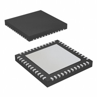
QFN-48
RGZ
–40°C to 85°C
ORDERING NUMBER
TRANSPORT MEDIA,
QUANTITY
TSC2117IRGZT
Tape and reel, 250
TSC2117IRGZR
Tape and reel, 2500
PACKAGE AND SIGNAL DESCRIPTIONS
Copyright © 2009–2012, Texas Instruments Incorporated
Submit Documentation Feedback
Product Folder Link(s): TSC2117
3
�TSC2117
SLAS550B – APRIL 2009 – REVISED JUNE 2012
2.2
www.ti.com
Device Information
37 SPRN
38 SRVDD
39 SRVSS
40 SPRP
41 HPL
42 HVDD
43 HVSS
44 HPR
45 GPI3
46 GPI2
47 GPI1
48 RESET
RGZ Package
(Top View)
MISO 1
36 SPLP
MOSI 2
35 SLVDD
SS 3
34 SLVSS
SCLK 4
33 SPLN
GPIO1 5
32 TSVDD
GPIO2 6
31 XP
TSC2117
IOVSS 7
30 YP
IOVDD 8
29 DVSS
DVDD 9
28 XN
SDOUT 10
27 YN
SDIN 11
26 TSVSS
WCLK 12
VBAT 24
AVDD 23
AVSS 22
AUX2 21
AUX1 20
MIC 19
MICBIAS 18
VOL/MICDET 17
SCL 16
SDA 15
MCLK 14
BCLK 13
25 VREF
P0023-17
Table 2-1. TERMINAL FUNCTIONS
TERMINAL
NAME
NO.
AUX1
20
AUX2
AVDD
AVSS
BCLK
I/O
DESCRIPTION
I
AUX1 (primary aux. input to SAR ADC), also routed to audio ADC input mixer and audio DAC
output mixer
21
I
AUX2 (secondary aux. input to SAR ADC), also routed to audio ADC input mixer
23
–
Analog power supply
22
–
Analog ground
13
I/O
DVDD
9
–
Digital power – digital core
DVSS
29
–
Digital ground (internally connected to HVSS)
GPI1
47
I
General-purpose input and multifunction pin
GPI2
46
I
General-purpose input and multifunction pin
GPI3
45
I
General-purpose input and multifunction pin
GPIO1
5
I/O
General-purpose input/output pin and multifunction pin
GPIO2
6
I/O
General-purpose input/output pin and multifunction pin
HPL
41
O
Left-channel headphone driver output
HPR
44
O
Right-channel headphone driver output
HVDD
42
–
Headphone driver and PLL power
HVSS
43
–
Driver and PLL ground (internally connected to DVSS)
4
Audio serial clock
PACKAGE AND SIGNAL DESCRIPTIONS
Copyright © 2009–2012, Texas Instruments Incorporated
Submit Documentation Feedback
Product Folder Link(s): TSC2117
�TSC2117
www.ti.com
SLAS550B – APRIL 2009 – REVISED JUNE 2012
Table 2-1. TERMINAL FUNCTIONS (continued)
TERMINAL
I/O
DESCRIPTION
NAME
NO.
IOVDD
8
–
Digital interface power
IOVSS
7
–
Digital interface ground
MCLK
14
I
External master clock
MIC
19
I
Microphone input (routed to audio ADC input mixer and audio DAC output mixer)
MICBIAS
18
O
Microphone bias voltage
MISO
1
O
Data output from SPI (Hi-Z capable)
MOSI
2
I
Data input to SPI
RESET
48
I
Reset for logic and all internal registers – active-low
SCL
16
I/O
SCLK
4
I
SDA
15
I/O
SDIN
11
I
Playback audio serial-data input
SDOUT
10
O
Record audio serial-data output (hi-Z capable)
SLVDD
35
–
Left-channel class-D speaker-amplifier power supply
SLVSS
34
–
Left-channel class-D speaker-amplifier power-supply ground
SPLN
33
O
Left-channel speaker-driver inverting output
SPLP
36
O
Left-channel speaker-driver noninverting output
SPRN
37
O
Right-channel speaker-driver inverting output
SPRP
40
O
Right-channel speaker-driver noninverting output
SRVDD
38
–
Right-channel class-D speaker-amplifier power supply
SRVSS
39
–
Right-channel class-D speaker-amplifier power-supply ground
SS
3
I
SPI chip select – active-low
TSVDD
32
–
Touch-screen controller power (used for touch-screen panel driver)
TSVSS
26
–
Touch-screen driver ground
VBAT
24
I
Battery-monitor input to SAR ADC
VOL/MICDET
17
I
Playback digital volume control or microphone-detection functionality
VREF
25
I/O
Voltage reference input for SAR ADC
WCLK
12
I/O
Audio serial-bus channel clock
XN
28
I/O
Touch-screen X– positional input and driver
XP
31
I/O
Touch-screen X+ positional input and driver
YN
27
I/O
Touch-screen Y– positional input and driver
YP
30
I/O
Touch-screen Y+ positional input and driver
I2C control bus clock input
External clock to SPI
I2C control-bus data I/O
ELECTRICAL SPECIFICATIONS
Copyright © 2009–2012, Texas Instruments Incorporated
Submit Documentation Feedback
Product Folder Link(s): TSC2117
5
�TSC2117
SLAS550B – APRIL 2009 – REVISED JUNE 2012
www.ti.com
3 ELECTRICAL SPECIFICATIONS
3.1
Absolute Maximum Ratings
over operating free-air temperature range (unless otherwise noted)
(1)
VALUE
UNIT
AVDD to AVSS
–0.3 to 3.9
V
DVDD to DVSS
–0.3 to 2.5
V
HVDD to HVSS
–0.3 to 3.9
V
SLVDD to SLVSS
–0.3 to 6
V
SRVDD to SRVSS
–0.3 to 6
V
–0.3 to 3.9
V
IOVDD to IOVSS
TSVDD to TSVSS
–0.3 to 3.9
V
AVSS – 0.3 to AVDD
V
Digital input voltage
IOVSS – 0.3 to IOVDD + 0.3
V
Analog input voltage
AVSS – 0.3 to AVDD + 0.3
V
VREF to AVSS
VBAT
–0.3 to 6
V
Operating temperature range
–40 to 85
°C
Storage temperature range
–55 to 150
°C
105
°C
Junction temperature (TJ Max)
Power dissipation
QFN package
Lead temperature
(1)
(TJ Max – TA)/RθJA
W
RθJA Thermal impedance (with thermal pad soldered to board)
27
°C/W
Infrared (15 s)
300
°C
Stresses beyond those listed under Absolute Maximum Ratings may cause permanent damage to the device. These are stress ratings
only, and functional operation of the device at these or any other conditions beyond those indicated under Recommended Operating
Conditions is not implied. Exposure to absolute-maximum-rated conditions for extended periods may affect device reliability.
Table 3-1. System Thermal Characteristics (1)
(1)
6
Power Rating at 25°C
Derating Factor
Power Rating at 70°C
Power Rating at 85°C
3W
37.04 mW/°C
1.3 W
0.74 W
This data was taken using 2-oz. (0.071-mm thick) trace and copper pad that is soldered to a JEDEC high-K, standard 4-layer 3-in. × 3
in. (7.62-cm × 7.62-cm) PCB.
ELECTRICAL SPECIFICATIONS
Copyright © 2009–2012, Texas Instruments Incorporated
Submit Documentation Feedback
Product Folder Link(s): TSC2117
�TSC2117
www.ti.com
3.2
SLAS550B – APRIL 2009 – REVISED JUNE 2012
Recommended Operating Conditions
over operating free-air temperature range (unless otherwise noted)
MIN
NOM
(2)
2.7
3.3
3.6
DVDD
Referenced to DVSS(2)
1.65
1.8
1.95
HVDD
Referenced to HVSS(2)
2.7
3.3
3.6
Referenced to SLVSS(2)
2.7
(2)
Referenced to SRVSS
2.7
TSVDD
Referenced to TSVSS(2)
2.7
3.3
3.6
IOVDD
Referenced to IOVSS(2)
1.1
3.3
3.6
3.3
AVDD
AVDD
(1)
SLVDD (1)
SRVDD
Power-supply voltage range
(1)
VREF
VI
MCLK (3)
SCLK
Referenced to AVSS
V
5.5
0
Speaker impedance
Resistance applied across class-D output pins
(BTL)
8
Ω
Headphone impedance
AC coupled to RL
16
Ω
Analog audio full-scale input
voltage
AVDD = 3.3V, single-ended
Stereo line output load
impedance
AC coupled to RL
Master clock frequency
IOVDD = 3.3V
50
MHz
SCLK frequency
IOVDD = 3.3V
30
MHz
SCLK duty cycle
Operating free-air temperature
V
0.707
VRMS
10
40%
SCL clock frequency
3.3
5.5
Referenced to AVSS
TA
(3)
UNIT
External voltage reference
SCL
(1)
(2)
(2)
MAX
50%
–40
kΩ
60%
400
kHz
85
°C
To minimize battery-current leakage, the SLVDD and SRVDD voltage levels should not be below the AVDD voltage level.
All grounds on board are tied together, so they should not differ in voltage by more than 0.2 V maximum for any combination of ground
signals. By use of a wide trace or ground plane, ensure a low-impedance connection between HVSS and DVSS.
The maximum input frequency should be 50 MHz for any digital pin used as a general-purpose clock.
Electrical Characteristics
At 25°C, AVDD, HVDD, IOVDD, TSVDD, = 3.3 V, SLVDD, SRVDD = 3.6V, DVDD = 1.8 V, VREF = 3.3 V, fS (audio) =
48 kHz, CODEC_CLKIN = 256 × fS, PLL = Off, SAR input is AUX1, VOL/MICDET pin disabled (unless otherwise noted)
PARAMETER
TEST CONDITIONS
MIN
TYP
MAX
UNIT
VREF
V
SAR CONVERTER
Auxilary Analog Input
Input voltage range
Input impedance
(1)
Input capacitance
0
1/(f×C)
AUX1, AUX2, VBAT input selected as input by touch
screen
Input leakage current
Input voltage range for VBAT
(1)
Battery-measurement mode
0
kΩ
25
pF
1
μA
6
V
SAR input impedance is dependent on the sampling frequency, where the sampling capacitor is C = 25 pF.
ELECTRICAL SPECIFICATIONS
Copyright © 2009–2012, Texas Instruments Incorporated
Submit Documentation Feedback
Product Folder Link(s): TSC2117
7
�TSC2117
SLAS550B – APRIL 2009 – REVISED JUNE 2012
www.ti.com
Electrical Characteristics (continued)
At 25°C, AVDD, HVDD, IOVDD, TSVDD, = 3.3 V, SLVDD, SRVDD = 3.6V, DVDD = 1.8 V, VREF = 3.3 V, fS (audio) =
48 kHz, CODEC_CLKIN = 256 × fS, PLL = Off, SAR input is AUX1, VOL/MICDET pin disabled (unless otherwise noted)
PARAMETER
TEST CONDITIONS
MIN
TYP
MAX
UNIT
Touch-Screen SAR ADC
INL
Resolution
Programmable: 8-bit, 10-bit, 12-bit
No missing codes
12-bit resolution
8
11
12
Bits
Bits
Integral nonlinearity
12-bit resolution, conversion clock = 2 MHz
±7
LSB
Offset error
12-bit resolution, conversion clock = 2 MHz
±7
LSB
Gain error
12-bit resolution, conversion clock = 2 MHz
±7
LSB
Noise
12-bit resolution, conversion clock = 2 MHz,
AUX2 = 1 Vdc
0.8
LSB
Conversion Rate
Normal conversion operation
12 bits, internal conversion clock = 2 MHz
119
kHz
High-speed conversion
operation
8 bits, internal conversion clock = 6 MHz (Conversion
accuracy is reduced.)
250
kHz
Voltage Reference—VREF
Voltage range
Internal VREF output voltage
Internal VREF
1.25
2.5
External VREF
1.25
AVDD
Measured with 1-μF capacitor to analog ground.
Internal VREF selected as 1.25 V (page 3/register 6,
bit D6 = 0)
V
1.23
V
8.2
MHz
INTERNAL OSCILLATOR—RC_CLK
Oscillator frequency for SAR
VOLUME CONTROL PIN (ADC); VOL/MICDET pin enabled
Input voltage range
VOL/MICDET pin configured as volume control (page
0/register 116, bit D7 = 1 and page 0/register 67, bit
D7 = 0)
0.5 ×
AVDD
0
Input capacitance
2
Volume control steps
V
pF
128
Steps
0.707
VRMS
AUDIO ADC
Microphone Input to ADC, 984-Hz Sine-Wave Input, fS = 48 kHz, AGC = OFF
Input signal level (0-dB)
MIC with R1 = 20 kΩ (page 1/register 48 and register
49, bits D7–D6)
Signal-to-noise ratio
fS = 48 kHz, 0-dB PGA gain, MIC input ac-shorted to
ground; measured as idle-channel noise,
A-weighted (1) (2)
Dynamic range
fS = 48 kHz, 0-dB PGA gain, MIC input 1 kHz at –60dBFS input applied, referenced to 0.707-Vrms input,
A-weighted (1) (2)
THD+N
Total harmonic distortion +
noise
fS = 48 kHz, 0-dB PGA gain, MIC input 1 kHz at –2
dBFS input applied, referenced to 0.707 Vrms input
–83
THD
Total harmonic distortion
fS = 48 kHz, 0-dB PGA gain, MIC input 1 kHz at –2
dBFS input applied, referenced to 0.707 Vrms input
–90
dB
Input capacitance
MIC input
2
pF
SNR
(1)
(2)
8
80
90
dB
91
dB
–70
dB
Ratio of output level with 1-kHz full-scale sine-wave input, to the output level with the inputs short-circuited, measured A-weighted over a
20-Hz to 20-kHz bandwidth using an audio analyzer.
All performance measurements done with 20-kHz low-pass filter and, where noted, A-weighted filter. Failure to use such a filter may
result in higher THD+N and lower SNR and dynamic range readings than shown in the Electrical Characteristics. The low-pass filter
removes out-of-band noise, which, although not audible, may affect dynamic specification values.
ELECTRICAL SPECIFICATIONS
Copyright © 2009–2012, Texas Instruments Incorporated
Submit Documentation Feedback
Product Folder Link(s): TSC2117
�TSC2117
www.ti.com
SLAS550B – APRIL 2009 – REVISED JUNE 2012
Electrical Characteristics (continued)
At 25°C, AVDD, HVDD, IOVDD, TSVDD, = 3.3 V, SLVDD, SRVDD = 3.6V, DVDD = 1.8 V, VREF = 3.3 V, fS (audio) =
48 kHz, CODEC_CLKIN = 256 × fS, PLL = Off, SAR input is AUX1, VOL/MICDET pin disabled (unless otherwise noted)
PARAMETER
TEST CONDITIONS
MIN
TYP
MAX
2.25
2.5
2.75
UNIT
Microphone Bias
Page 1/register 46, bits D1–D0 = 10
Voltage output
Voltage regulation
Page 1/register 46, bits D1–D0 = 01
2
At 4-mA load current, page 1/register 46, bits D1–D0
= 10 (MICBIAS = 2.5 V)
5
At 4-mA load current, page 1/register 46, bits D1–D0
= 01 (MICBIAS = 2 V)
7
V
mV
Audio ADC Digital Decimation Filter Characteristics
See Section 5.5.4.4 for audio ADC decimation filter characteristics.
DAC HEADPHONE OUTPUT, AC-coupled load = 16 Ω (single-ended),
driver gain = 0 dB, parasitic capacitance = 30 pF
Full-scale output voltage (0
dB)
Output common-mode setting = 1.65 V
0.707
(1) (2)
SNR
Signal-to-noise ratio
Measured as idle-channel noise, A-weighted
THD
Total harmonic distortion
0-dBFS input
–85
–65
dB
THD+N
Total harmonic distortion +
noise
0-dBFS input
–82
–60
dB
Mute attenuation
PSRR
PO
Power-supply rejection ratio
Maximum output power
(3)
80
Vrms
95
dB
87
dB
Ripple on HVDD (3.3 V) = 200 mVp-p at 1 kHz
62
dB
RL = 32 Ω, THD+N ≤ –60 dB
20
RL = 16 Ω, THD+N ≤ –60 dB
60
mW
DAC LINEOUT (HP Driver in Lineout Mode)
SNR
Signal-to-noise ratio
Measured as idle-channel noise, A-weighted
95
dB
THD
Total harmonic distortion
0-dBFS input, 0-dB gain
–86
dB
THD+N
Total harmonic distortion +
noise
0-dBFS input, 0-dB gain
–82
dB
DAC Digital Interpolation Filter Characteristics
See Section 5.6.1.4 for DAC interpolation filter characteristics.
DAC OUTPUT to CLASS-D SPEAKER OUTPUT; Load = 8 Ω (differential), 50 pF
Output voltage
SNR
(1)
(2)
(3)
SLVDD = SRVDD = 3.6 V, BTL measurement, DAC
input = 0 dBFS, DAC VCM (page 1/register 31, bits
D4–D3) = 1.65 V, class-D gain = 6 dB,
THD ≤ –16.5 dB
2.2
SLVDD = SRVDD = 3.6 V, BTL measurement, DAC
input = –2 dBFS, DAC VCM (page 1/register 31, bits
D4–D3) = 1.65 V, class-D gain = 6 dB, THD ≤ –20 dB
2.1
Output, common-mode
SLVDD = SRVDD = 3.6 V, BTL measurement, DAC
input = mute, DAC VCM (page 1/register 31, bits
D4–D3) = 1.65 V, class-D gain = 6 dB
Signal-to-noise ratio
SLVDD = SRVDD = 3.6 V, BTL measurement, classD gain = 6 dB, measured as idle-channel noise, Aweighted (with respect to full-scale output value of 2.2
Vrms) (1) (2)
Vrms
1.65
V
87
dB
Ratio of output level with 1-kHz full-scale sine-wave input, to the output level with the inputs short-circuited, measured A-weighted over a
20-Hz to 20-kHz bandwidth using an audio analyzer.
All performance measurements done with 20-kHz low-pass filter and, where noted, A-weighted filter. Failure to use such a filter may
result in higher THD+N and lower SNR and dynamic range readings than shown in the Electrical Characteristics. The low-pass filter
removes out-of-band noise, which, although not audible, may affect dynamic specification values.
é VSIGSupp ù
PSRR = 20 log10 ê
ú
ëê VDACOUT ûú
DAC to headphone-out PSRR measurement is calculated as
ELECTRICAL SPECIFICATIONS
Copyright © 2009–2012, Texas Instruments Incorporated
Submit Documentation Feedback
Product Folder Link(s): TSC2117
9
�TSC2117
SLAS550B – APRIL 2009 – REVISED JUNE 2012
www.ti.com
Electrical Characteristics (continued)
At 25°C, AVDD, HVDD, IOVDD, TSVDD, = 3.3 V, SLVDD, SRVDD = 3.6V, DVDD = 1.8 V, VREF = 3.3 V, fS (audio) =
48 kHz, CODEC_CLKIN = 256 × fS, PLL = Off, SAR input is AUX1, VOL/MICDET pin disabled (unless otherwise noted)
PARAMETER
TEST CONDITIONS
MIN
TYP
MAX
UNIT
DAC OUTPUT to CLASS-D SPEAKER OUTPUT; Load = 8 Ω (differential), 50 pF (continued)
THD
Total harmonic distortion
SLVDD = SRVDD = 3.6 V, BTL measurement, DAC
input = –6 dBFS, DAC VCM (page 1/register 31, bits
D4–D3) = 1.65 V, class-D gain = 6 dB
–72
dB
THD+N
Total harmonic distortion +
noise
SLVDD = SRVDD = 3.6 V, BTL measurement, DAC
input = –6 dBFS, DAC VCM (page 1/register 31, bits
D4–D3) = 1.65 V, class-D gain = 6 dB
–71
dB
PSRR
Power-supply rejection ratio (1)
SLVDD = SRVDD = 3.6 V, BTL measurement, ripple
on SLVDD/SRVDD = 200 mVp-p at 1 kHz
57
dB
110
dB
Mute attenuation
PO
Maximum output power
Output-stage leakage current
for direct battery connection
SLVDD = SRVDD = 3.6 V, BTL measurement, DAC
VCM (page 1/register 31, bits D4–D3) = 1.65 V,
class-D gain = 18 dB, THD = 10%
540
SLVDD = SRVDD = 4.3 V, BTL measurement, DAC
VCM (page 1/register 31, bits D4–D3) = 1.65 V,
class-D gain = 18 dB, THD = 10%
790
SLVDD = SRVDD = 5.5 V, BTL measurement, DAC
VCM (page 1/register 31, bits D4–D3) = 1.65 V,
class-D gain = 18 dB, THD = 10%
1.29
W
SLVDD = SRVDD = 4.3 V, device is powered down
(power-up-reset condition)
80
nA
mW
ADC and DAC POWER CONSUMPTION
For ADC and DAC power consumption based per selected processing block, see Section 5.4
DIGITAL INPUT/OUTPUT
Logic
family
CMOS
VIH
VIL
Logic level
IIH = 5 μA, IOVDD ≥ 1.6 V
0.7 ×
IOVDD
IIH = 5 μA, IOVDD < 1.6 V
IOVDD
IIL = 5 μA, IOVDD ≥ 1.6 V
–0.3
IOH = 2 TTL loads
VOL
IOL = 2 TTL loads
0.8 ×
IOVDD
V
0.1 ×
IOVDD
10
PSRR + 20 log10
DAC to speaker-out PSRR measurement is calculated as
V
0
Capacitive load
10
0.3 ×
IOVDD
IIL = 5 μA, IOVDD < 1.6 V
VOH
(1)
V
ƪ
VSIG Supp
V SPK1ń2
ELECTRICAL SPECIFICATIONS
ƫ
V
pF
.
Copyright © 2009–2012, Texas Instruments Incorporated
Submit Documentation Feedback
Product Folder Link(s): TSC2117
�TSC2117
www.ti.com
3.4
3.4.1
SLAS550B – APRIL 2009 – REVISED JUNE 2012
Timing Characteristics
I2S/LJF/RJF Timing in Master Mode
All specifications at 25°C, DVDD = 1.8 V
Note: All timing specifications are measured at characterization but not tested at final test.
WCLK
tr
td(WS)
BCLK
td(DO-WS)
tf
td(DO-BCLK)
SDOUT
tS(DI)
th(DI)
SDIN
T0145-06
PARAMETER
td(WS)
td(DO-WS)
td(DO-BCLK)
ts(DI)
th(DI)
tr
tf
WCLK delay
WCLK to DOUT delay (for LJF mode only)
BCLK to DOUT delay
SDIN setup
SDIN hold
Rise time
Fall time
IOVDD = 1.1 V
MIN
MAX
45
45
45
8
8
25
25
IOVDD = 3.3 V
MIN
MAX
20
20
20
6
6
10
10
UNITS
ns
ns
ns
ns
ns
ns
ns
Figure 3-1. I2S/LJF/RJF Timing in Master Mode
ELECTRICAL SPECIFICATIONS
Copyright © 2009–2012, Texas Instruments Incorporated
Submit Documentation Feedback
Product Folder Link(s): TSC2117
11
�TSC2117
SLAS550B – APRIL 2009 – REVISED JUNE 2012
3.4.2
www.ti.com
I2S/LJF/RJF Timing in Slave Mode
All specifications at 25°C, DVDD = 1.8 V
Note: All timing specifications are measured at characterization but not tested at final test.
WCLK
tr
th(WS)
tS(WS)
tH(BCLK)
BCLK
td(DO-WS)
tL(BCLK)
tf
td(DO-BCLK)
SDOUT
tS(DI)
th(DI)
SDIN
T0145-07
PARAMETER
tH(BCLK)
tL(BCLK)
ts(WS)
th(WS)
td(DO-WS)
td(DO-BCLK)
ts(DI)
th(DI)
tr
tf
BCLK high period
BCLK low period
WCLK setup
WCLK hold
WCLK to DOUT delay (for LJF mode only)
BCLK to DOUT delay
SDIN setup
SDIN hold
Rise time
Fall time
IOVDD = 1.1 V
MIN
MAX
35
35
8
8
45
45
8
8
4
4
IOVDD = 3.3 V
MIN
MAX
35
35
6
6
20
20
6
6
4
4
UNIT
ns
ns
ns
ns
ns
ns
ns
ns
ns
ns
Figure 3-2. I2S/LJF/RJF Timing in Slave Mode
12
ELECTRICAL SPECIFICATIONS
Copyright © 2009–2012, Texas Instruments Incorporated
Submit Documentation Feedback
Product Folder Link(s): TSC2117
�TSC2117
www.ti.com
3.4.3
SLAS550B – APRIL 2009 – REVISED JUNE 2012
DSP Timing in Master Mode
All specifications at 25°C, DVDD = 1.8 V
Note: All timing specifications are measured at characterization but not tested at final test.
WCLK
td(WS)
td(WS)
tf
BCLK
tr
td(DO-BCLK)
SDOUT
tS(DI)
th(DI)
SDIN
T0146-05
IOVDD = 1.1 V
MIN
MAX
45
45
8
8
25
25
PARAMETER
td(WS)
td(DO-BCLK)
ts(DI)
th(DI)
tr
tf
WCLK delay
BCLK to DOUT delay
SDIN setup
SDIN hold
Rise time
Fall time
IOVDD = 3.3 V
MIN
MAX
20
20
8
8
10
10
UNITS
ns
ns
ns
ns
ns
ns
Figure 3-3. DSP Timing in Master Mode
ELECTRICAL SPECIFICATIONS
Copyright © 2009–2012, Texas Instruments Incorporated
Submit Documentation Feedback
Product Folder Link(s): TSC2117
13
�TSC2117
SLAS550B – APRIL 2009 – REVISED JUNE 2012
3.4.4
www.ti.com
DSP Timing in Slave Mode
All specifications at 25°C, DVDD = 1.8 V
Note: All timing specifications are measured at characterization but not tested at final test.
WCLK
tS(WS)
tS(WS)
th(WS)
th(WS)
tf
tL(BCLK)
BCLK
tr
td(DO-BCLK)
tH(BCLK)
SDOUT
tS(DI)
th(DI)
SDIN
T0146-06
IOVDD = 1.1 V
MIN
MAX
35
35
8
8
45
8
8
4
4
PARAMETER
tH(BCLK)
tL(BCLK)
ts(WS)
th(WS)
td(DO-BCLK)
ts(DI)
th(DI)
tr
tf
BCLK high period
BCLK low period
WCLK setup
WCLK hold
BCLK to DOUT delay
SDIN setup
SDIN hold
Rise time
Fall time
IOVDD = 3.3 V
MIN
MAX
35
35
8
8
20
8
8
4
4
UNITS
ns
ns
ns
ns
ns
ns
ns
ns
ns
Figure 3-4. DSP Timing in Slave Mode
14
ELECTRICAL SPECIFICATIONS
Copyright © 2009–2012, Texas Instruments Incorporated
Submit Documentation Feedback
Product Folder Link(s): TSC2117
�TSC2117
www.ti.com
3.4.5
SLAS550B – APRIL 2009 – REVISED JUNE 2012
I2C Interface Timing
All specifications at 25°C, DVDD = 1.8 V
Note: All timing specifications are measured at characterization but not tested at final test.
SDA
tBUF
tLOW
tr
tHIGH
tf
tHD;STA
SCL
tHD;STA
tSU;DAT
tHD;DAT
STO
tSU;STO
tSU;STA
STA
STA
STO
T0295-02
PARAMETER
fSCL
tHD;STA
tLOW
tHIGH
tSU;STA
tHD;DAT
tSU;DAT
tr
tf
tSU;STO
tBUF
Cb
SCL clock frequency
Hold time (repeated) START condition.
After this period, the first clock pulse is
generated.
LOW period of the SCL clock
HIGH period of the SCL clock
Setup time for a repeated START
condition
Data hold time: For I2C bus devices
Data set-up time
SDA and SCL Rise Time
SDA and SCL Fall Time
Set-up time for STOP condition
Bus free time between a STOP and
START condition
Capacitive load for each bus line
Standard-Mode
MIN
TYP
0
4.0
MAX
100
4.7
4.0
4.7
0
250
Fast-Mode
MIN
TYP
0
0.8
UNITS
MAX
400
μs
μs
μs
1.3
0.6
0.8
3.45
1000
300
4.0
4.7
400
0
100
20 + 0.1Cb
20 + 0.1Cb
0.8
1.3
kHz
μs
300
300
μs
ns
ns
ns
μs
μs
400
pF
0.9
Figure 3-5. I2C Interface Timing
ELECTRICAL SPECIFICATIONS
Copyright © 2009–2012, Texas Instruments Incorporated
Submit Documentation Feedback
Product Folder Link(s): TSC2117
15
�TSC2117
SLAS550B – APRIL 2009 – REVISED JUNE 2012
3.4.6
www.ti.com
SPI Interface Timing
All specifications at 25°C, DVDD = 1.8 V
Note: All timing specifications are measured at characterization but not tested at final test.
SS
S
t
t Lead
t Lag
t
td
sck
SCLK
t wsck
tf
tr
t wsck
tv
MISO
t ho
MSB OUT
t dis
BIT 6 . . . 1
LSB OUT
ta
t hi
t su
MOSI
MSB IN
PARAMETER
twsck
tLead
tLag
ttd
ta
tdis
tsu
thi
tv
tr
tf
SCLK pulse duration
Enable lead time
Enable lag time
Sequential transfer delay
MISO slave data-out access time
MISO slave data-out disable time
MOSI dataiin setup time
MOSI data-in hold time
MISO data-valid time
SCLK rise time
SCLK fall time
BIT 6 . . . 1
IOVDD = 1.1 V
MIN
50
50
50
40
LSB IN
IOVDD = 3.3 V
MIN
20
20
20
20
MAX
40
40
MAX
20
20
15
15
10
10
25
4
4
18
4
4
UNITS
ns
ns
ns
ns
ns
ns
ns
ns
ns
ns
ns
Figure 3-6. SPI Interface Timing Diagram
16
ELECTRICAL SPECIFICATIONS
Copyright © 2009–2012, Texas Instruments Incorporated
Submit Documentation Feedback
Product Folder Link(s): TSC2117
�TSC2117
www.ti.com
SLAS550B – APRIL 2009 – REVISED JUNE 2012
4 TYPICAL PERFORMANCE
4.1
Audio ADC Performance
AMPLITUDE
vs
FREQUENCY
AMPLITUDE
vs
FREQUENCY
0
0
AVDD = HVDD = TSVDD
= IOVDD = SVDD = 3.3 V
DVDD = 1.8 V
−20
−40
Amplitude − dBFS
−40
Amplitude − dBFS
AVDD = HVDD = TSVDD
= IOVDD = SVDD = 3.3 V
DVDD = 1.8 V
−20
−60
−80
−100
−60
−80
−100
−120
−120
−140
−140
−160
−160
0
5
10
15
20
0
5
f − Frequency − kHz
10
15
G018
G019
Figure 4-1. FFT - ADC Idle Channel Differential
Figure 4-2. FFT- ADC Single-Ended Input
AMPLITUDE
vs
FREQUENCY
AMPLITUDE
vs
FREQUENCY
0
0
AVDD = HVDD = TSVDD
= IOVDD = SVDD = 3.3 V
DVDD = 1.8 V
−20
AVDD = HVDD = TSVDD
= IOVDD = SVDD = 3.3 V
DVDD = 1.8 V
−20
−40
Amplitude − dBFS
−40
Amplitude − dBFS
20
f − Frequency − kHz
−60
−80
−100
−60
−80
−100
−120
−120
−140
−140
−160
−160
0
5
10
15
20
0
f − Frequency − kHz
5
10
15
20
f − Frequency − kHz
G017
Figure 4-3. FFT - ADC Differential Input
G020
Figure 4-4. FFT - ADC Idle Channel Single-Ended
TYPICAL PERFORMANCE
Copyright © 2009–2012, Texas Instruments Incorporated
Submit Documentation Feedback
Product Folder Link(s): TSC2117
17
�TSC2117
SLAS550B – APRIL 2009 – REVISED JUNE 2012
www.ti.com
SNR
vs
PGA CHANNEL GAIN
100
95
Diff = 10k
90
Diff = 20k
SNR − dB
85
80
Diff = 40k
75
SE = 10k
70
65
SE = 20k
60
55
SE = 40k
50
−10
0
10
20
30
40
50
60
70
Channel Gain − dB
G022
Figure 4-5.
4.2
DAC Performance
AMPLITUDE
vs
FREQUENCY
0
0
−20
−20
−40
−40
Amplitude − dBFS
Amplitude − dBFS
AMPLITUDE
vs
FREQUENCY
−60
−80
−100
−60
−80
−100
−120
−120
−140
−140
−160
−160
0
5
10
15
20
0
f − Frequency − kHz
5
10
15
20
f − Frequency − kHz
G023
Figure 4-6. FFT - DAC to Line Output
18
G026
Figure 4-7. FFT - DAC to Headphone Output
TYPICAL PERFORMANCE
Copyright © 2009–2012, Texas Instruments Incorporated
Submit Documentation Feedback
Product Folder Link(s): TSC2117
�TSC2117
www.ti.com
SLAS550B – APRIL 2009 – REVISED JUNE 2012
TOTAL HARMONIC DISTORTION + NOISE
vs
OUTPUT POWER
THD+N − Total Harmonic Distortion + Noise − dB
0
RL = 16 Ω
HVDD = 2.7 V
CM = 1.35 V
−10
−20
−30
−40
HVDD = 3 V
CM = 1.5 V
−50
−60
HVDD = 3.3 V
CM = 1.65 V
−70
−80
HVDD = 3.6 V
CM = 1.8 V
−90
0.00
0.02
0.04
0.06
0.08
0.10
0.12
0.14
PO − Output Power − W
G025
Figure 4-8. Headphone Output Power (RL = 16 Ω)
4.3
Class-D Speaker Driver Performance
TOTAL HARMONIC DISTORTION + NOISE
vs
OUTPUT POWER
TOTAL HARMONIC DISTORTION + NOISE
vs
OUTPUT POWER
−10
−20
0
THD+N − Total Harmonic Distortion + Noise − dB
THD+N − Total Harmonic Distortion + Noise − dB
0
AVDD = HVDD = TSVDD
= IOVDD = 3.3 V
SVDD = 5.5 V
DVDD = 1.8 V
−30
12 dB
−40
−50
−60
24 dB
18 dB
−70
6 dB
−80
0.0
0.5
1.0
1.5
PO − Output Power − W
2.0
SLVDD = 3.3 V
−10
−20
−40
−50
SLVDD = 4.3 V
−60
SLVDD = 5.5 V
−70
−80
0.0
RL = 8 Ω
0.5
1.0
1.5
PO − Output Power − W
G014
Figure 4-9. Max Class-D Speaker-Driver Output
Power (RL = 8 Ω, Driver Gain = 6 dB to 24 dB)
SLVDD = 3.6 V
−30
2.0
G015
Figure 4-10. Class-D Speaker-Driver Output Power
(RL = 8 Ω, SLVDD = 3.3 V to 5.5V, Driver Gain = 18
dB)
TYPICAL PERFORMANCE
Copyright © 2009–2012, Texas Instruments Incorporated
Submit Documentation Feedback
Product Folder Link(s): TSC2117
19
�TSC2117
SLAS550B – APRIL 2009 – REVISED JUNE 2012
4.4
www.ti.com
Analog Bypass Performance
AMPLITUDE
vs
FREQUENCY
0
0
−20
−20
−40
−40
Amplitude − dBFS
Amplitude − dBFS
AMPLITUDE
vs
FREQUENCY
−60
−80
−100
−60
−80
−100
−120
−120
−140
−140
−160
−160
0
5
10
15
20
0
5
f − Frequency − kHz
10
G024
Figure 4-11. FFT - Line In Bypass to Line Output
4.5
15
20
f − Frequency − kHz
G027
Figure 4-12. FFT - Line In Bypass to Headphone
Output
MICBIAS Performance
VOLTAGE
vs
CURRENT
3.5
3.0
Micbias = AVDD (3.3 V)
V − Voltage − V
2.5
Micbias = 2.5 V
2.0
Micbias = 2 V
1.5
1.0
0.5
0.0
0.0
0.5
1.0
1.5
2.0
2.5
3.0
3.5
4.0
I − Current − mA
G016
Figure 4-13. Micbias
20
TYPICAL PERFORMANCE
Copyright © 2009–2012, Texas Instruments Incorporated
Submit Documentation Feedback
Product Folder Link(s): TSC2117
�TSC2117
www.ti.com
SLAS550B – APRIL 2009 – REVISED JUNE 2012
5 APPLICATION INFORMATION
5.1
Typical Circuit Configuration
+3.3VA
SVDD
0.1 mF
22 mF
0.1 mF
SLVDD SRVDD
8W
0.1 mF
22 mF
0.1 mF
10 mF
10 mF
HVDD AVDD
SLVSS SRVSS
AVSS
HVSS
GPIO1
SPLP
SPLN
GPIO2
Speakers
GPI1
8W
SPRP
SPRN
GPI2
GPI2
VOL/MICDET
SDA
2.2 kW
MICBIAS
SCL
0.1 mF
MIC
47 mF
HOST PROCESSOR
MCLK
HPL
Headset
47 mF
HPR
SDOUT
TSC2117
WCLK
SDIN
BCLK
1 mF
AUX1
Analog_In1
1 mF
RESET
AUX2
Analog_In2
System
Battery
SS
SVDD
Note: VBAT is used for
voltage measurement.
Touch
Screen
SCLK
VBAT
MOSI
MISO
XP
YP
XN
YN
2
4 ´ 0.1 mF
TSVDD
TSVSS
VREF
DVDD
DVSS
IOVDD
IOVSS
Note: Either I C
or SPI or both can
be used in any
mode. It is not
recommended to
2
+3.3VA
0.1 mF
+1.8VD
10 mF
10 mF
0.1 mF
use I C and SPI
simultaneously.
IOVDD
10 mF
0.1 mF
10 mF
Note: VREF can also be
supplied externally.
S0400-01
Figure 5-1. Typical Circuit Configuration
APPLICATION INFORMATION
Copyright © 2009–2012, Texas Instruments Incorporated
Submit Documentation Feedback
Product Folder Link(s): TSC2117
21
�TSC2117
SLAS550B – APRIL 2009 – REVISED JUNE 2012
5.2
www.ti.com
Overview
The TSC2117 is a highly integrated stereo audio DAC and monaural ADC with touch-screen controller for
portable computing, communication, and entertainment applications. A register-based architecture eases
integration with microprocessor-based systems through standard serial-interface buses. This device
supports the four-wire SPI bus and the 2-wire I2C bus interfaces. The I2C interface and the SPI interface
provide full register access. The SPI data bus can be used for higher-speed communication and for highspeed retrieval of SAR ADC data. All peripheral functions are controlled through these registers and the
onboard state machines.
The TSC2117 consists of the following blocks:
• Touch-panel drivers
• Microphone interfaces (analog and digital)
• Audio codec (mono ADC and stereo DAC)
• AGC and DRC
• Two miniDSP digital signal-processing blocks (record and playback paths)
• Beep generator
• Stereo headphone/lineout amplifier
• Class-D stereo amplifier for 8-Ω speakers
• Pin-controlled or register-controlled volume level
• Power-down de-pop and power-up soft start
• SAR ADC for touch-panel, voltage, and temperature measurements
• FIFO buffer mode for SAR auxiliary and touch-screen data
• Auxiliary inputs
• SPI control interface
• I2C control interface
• Power-down control block
Following a toggle of the RESET pin or a software reset, the device operates in the default mode. The SPI
or I2C interface can be used to write to the control registers to configure the device.
The I2C address assigned to the TSC2117 is 001 1000. This device always operates in an I2C slave
mode. All registers are 8-bit, and all writable registers have read-back capability. The device autoincrements to support sequential addressing and can be used with I2C fast mode. Once the device is
reset, all appropriate registers are updated by the host processor to configure the device as needed by the
user.
SAR ADC data is transferred though the SPI/I2C bus, and audio data (for audio ADC and DAC) is
transferred through the audio serial interface. The SPI interface requires that the SS signal be driven low
to communicate with the TSC2117. Data is then shifted into or out of the TSC2117 under control of the
host microprocessor, which also provides the SPI serial clock.
5.2.1
Device Initialization
5.2.1.1
Reset
The TSC2117 internal logic must be initialized to a known condition for proper device function. To initialize
the device to its default operating condition, the hardware reset pin (RESET) must be pulled low for at
least 10 ns. For this initialization to work, both the IOVDD and DVDD supplies must be powered up. It is
recommended that while the DVDD supply is being powered up, the RESET pin be pulled low.
The device can also be reset via software reset. Writing a 1 into page 0/register 1, bit D0 resets the
device.
22
APPLICATION INFORMATION
Copyright © 2009–2012, Texas Instruments Incorporated
Submit Documentation Feedback
Product Folder Link(s): TSC2117
�TSC2117
www.ti.com
5.2.1.2
SLAS550B – APRIL 2009 – REVISED JUNE 2012
Device Start-Up Lockout Times
After the TSC2117 is initialized through hardware reset at power-up or software reset, the internal
memories are initialized to default values. This initialization takes place within 1 ms after pulling the
RESET signal high. During this initialization phase, no register-read or register-write operation should be
performed on ADC or DAC coefficient buffers. Also, no block within the codec should be powered up
during the initialization phase.
5.2.1.3
PLL Start-Up
Whenever the PLL is powered up, a start-up delay of approximately of 10 ms occurs after the power-up
command of the PLL and before the clocks are available to the codec. This delay is to ensure stable
operation of the PLL and clock-divider logic.
5.2.1.4
Power-Stage Reset
The power-stage-only reset is used to reset the device after an overcurrent latching shutdown has
occurred. Using this reset re-enables the output stage without resetting all of the registers in the device.
Each of the four power stages has its own dedicated reset bit. The headphone power-stage reset is
performed by setting page 1/register 31, bit D7 for HPL and by setting page 1/register 31, bit D6 for HPR.
The speaker power-stage reset is performed by setting page 1/register 32, bit D7 for SPLP and SPLN,
and by setting page 1/register 32, bit D6 for SPRP and SPRN.
5.2.1.5
Software Power Down
By default, all circuit blocks are powered down following a reset condition. Hardware power up of each
circuit block can be controlled by writing to the appropriate control register. This approach allows the
lowest power-supply current for the functionality required. However, when a block is powered down, all of
the register settings are maintained as long as power is still being applied to the device. The TSC2117
touch-detection circuitry is enabled by default, and it can be powered down by writing to page 3/register 4,
bit D7.
5.2.2
Audio Analog I/O
The TSC2117 has a stereo audio DAC and a monaural ADC. It supports a wide range of analog interfaces
to support different headsets and analog outputs. The TSC2117 has features to interface output drivers
(8-Ω, 16-Ω, 32-Ω) and a microphone PGA with AGC control. A special circuit has also been included in
the TSC2117 to insert a short key-click sound into the stereo audio output. The key-click sound is used to
provide feedback to the user when a particular button is pressed or item is selected. The specific sound of
the keyclick can be adjusted by varying several register bits that control its frequency, duration, and
amplitude. See Key-Click Functionality With Beep Generator, Section 5.6.5.
5.3
miniDSP
The TSC2117 features two miniDSP cores. The first miniDSP core is tightly coupled to the ADC; the
second miniDSP core is tightly coupled to the DAC. The fully programmable algorithms for the miniDSP
must be loaded into the device after power up. The miniDSPs have direct access to the digital stereo
audio stream on the ADC and on the DAC side, offering the possibility for advanced, very low-group-delay
DSP algorithms.
The ADC miniDSP has 384 programmable instructions, 256 data memory locations, and 128
programmable coefficients. The DAC miniDSP has 1024 programmable instructions, 896 data memory
locations, and 512 programmable coefficients (in the adaptive mode, each bank has 256 programmable
coefficients).
APPLICATION INFORMATION
Copyright © 2009–2012, Texas Instruments Incorporated
Submit Documentation Feedback
Product Folder Link(s): TSC2117
23
�TSC2117
SLAS550B – APRIL 2009 – REVISED JUNE 2012
5.3.1
www.ti.com
Software
Software development for the TSC2117 is supported through TI's comprehensive PurePath™ Studio
software development environment, a powerful, easy-to-use tool designed specifically to simplify software
development on Texas Instruments miniDSP audio platforms. The graphical development environment
consists of a library of common audio functions that can be dragged and dropped into an audio signal flow
and graphically connected together. The DSP code can then be assembled from the graphical signal flow
with the click of a mouse.
See the TSC2117 product folder on www.ti.com to learn more about PurePath Studio and the latest status
on available, ready-to-use DSP algorithms.
5.4
Digital Processing Low-Power Modes
The TSC2117 device can be tuned to minimize power dissipation, to maximize performance, or to an
operating point between the two extremes to best fit the application. The choice of processing blocks,
PRB_P1 to PRB_P25 for stereo playback and PRB_R4 to PRB_R18 for mono recording, also influences
the power consumption. In fact, the numerous processing blocks have been implemented to offer a choice
among configurations having a different balance of power-optimization and signal-processing capabilities.
5.4.1
ADC, Mono, 48 kHz, DVDD = 1.8 V, AVDD = 3.3 V
AOSR = 128, Processing Block = PRB_R4 (Decimation Filter A)
Power consumption = 9.01 mW
Table 5-1. PRB_R4 Alternative Processing Blocks, 9.01 mW
Processing Block
Filter
Estimated Power Change (mW)
PRB_R5
A
0.23
PRB_R6
A
0.22
AOSR = 64, Processing Block = PRB_R11 (Decimation Filter B)
Power consumption = 7.99 mW
Table 5-2. PRB_R11 Alternative Processing Blocks, 7.99 mW
5.4.2
Processing Block
Filter
Estimated Power Change (mW)
PRB_R4
A
0.43
PRB_R5
A
0.67
PRB_R6
A
0.66
PRB_R10
B
–0.14
PRB_R12
B
0.04
ADC, Mono, 8 kHz, DVDD = 1.8 V, AVDD = 3.3 V
AOSR = 128, Processing Block = PRB_R4 (Decimation Filter A)
Power consumption = 6.77 mW
Table 5-3. PRB_R4 Alternative Processing Blocks, 6.77 mW
24
Processing Block
Filter
Estimated Power Change (mW)
PRB_R5
A
0.03
PRB_R6
A
0.03
APPLICATION INFORMATION
Copyright © 2009–2012, Texas Instruments Incorporated
Submit Documentation Feedback
Product Folder Link(s): TSC2117
�TSC2117
www.ti.com
SLAS550B – APRIL 2009 – REVISED JUNE 2012
AOSR = 64, Processing Block = PRB_R11 (Decimation Filter B)
Power consumption = 6.61 mW
Table 5-4. PRB_R11 Alternative Processing Blocks, 6.61 mW
5.4.3
Processing Block
Filter
Estimated Power Change (mW)
PRB_R4
A
0.07
PRB_R5
A
0.11
PRB_R6
A
0.11
PRB_R10
B
–0.02
PRB_R12
B
0.01
DAC Playback on Headphones, Stereo, 48 kHz, DVDD = 1.8 V, AVDD = 3.3 V,
HVDD = 3.3 V
DOSR = 128, Processing Block = PRB_P7 (Interpolation Filter B)
Power consumption = 24.28 mW
Table 5-5. PRB_P7 Alternative Processing Blocks, 24.28 mW
Processing Block
Filter
Estimated Power Change (mW)
PRB_P1
A
1.34
PRB_P2
A
2.86
PRB_P3
A
2.11
PRB_P8
B
1.18
PRB_P9
B
0.53
PRB_P10
B
1.89
PRB_P11
B
0.87
PRB_P23
A
1.48
PRB_P24
A
2.89
PRB_P25
A
3.23
DOSR = 64, Processing Block = PRB_P7 (Interpolation Filter B)
Power consumption = 24.5 mW
Table 5-6. PRB_P7 Alternative Processing Blocks, 24.5 mW
Processing Block
Filter
Estimated Power Change (mW)
PRB_P1
A
1.17
PRB_P2
A
2.62
PRB_P3
A
2
PRB_P8
B
0.99
PRB_P9
B
0.5
PRB_P10
B
1.46
PRB_P11
B
0.66
PRB_P23
A
1.43
PRB_P24
A
2.69
PRB_P25
A
2.92
APPLICATION INFORMATION
Copyright © 2009–2012, Texas Instruments Incorporated
Submit Documentation Feedback
Product Folder Link(s): TSC2117
25
�TSC2117
SLAS550B – APRIL 2009 – REVISED JUNE 2012
5.4.4
www.ti.com
DAC Playback on Headphones, Mono, 48 kHz, DVDD = 1.8 V, AVDD = 3.3 V,
HVDD = 3.3 V
DOSR = 128, Processing Block = PRB_P12 (Interpolation Filter B)
Power consumption = 15.4 mW
Table 5-7. PRB_P12 Alternative Processing Blocks, 15.4 mW
Processing Block
Filter
Estimated Power Change (mW)
PRB_P4
A
0.57
PRB_P5
A
1.48
PRB_P6
A
1.08
PRB_P13
B
0.56
PRB_P14
B
0.27
PRB_P15
B
0.89
PRB_P16
B
0.31
DOSR = 64, Processing Block = PRB_P12 (Interpolation Filter B)
Power consumption = 15.54 mW
Table 5-8. PRB_P12 Alternative Processing Blocks, 15.54 mW
5.4.5
Processing Block
Filter
Estimated Power Change (mW)
PRB_P4
A
0.37
PRB_P5
A
1.23
PRB_P6
A
1.15
PRB_P13
B
0.43
PRB_P14
B
0.13
PRB_P15
B
0.85
PRB_P16
B
0.21
DAC Playback on Headphones, Stereo, 8 kHz, DVDD = 1.8 V, AVDD = 3.3 V,
HVDD = 3.3 V
DOSR = 768, Processing Block = PRB_P7 (Interpolation Filter B)
Power consumption = 22.44 mW
Table 5-9. PRB_P7 Alternative Processing Blocks, 22.44 mW
26
Processing Block
Filter
Estimated Power Change (mW)
PRB_P1
A
0.02
PRB_P2
A
0.31
PRB_P3
A
0.23
PRB_P8
B
0.28
PRB_P9
B
–0.03
PRB_P10
B
0.14
PRB_P11
B
0.05
PRB_P23
A
0.29
PRB_P24
A
0.26
PRB_P25
A
0.47
APPLICATION INFORMATION
Copyright © 2009–2012, Texas Instruments Incorporated
Submit Documentation Feedback
Product Folder Link(s): TSC2117
�TSC2117
www.ti.com
SLAS550B – APRIL 2009 – REVISED JUNE 2012
DOSR = 384, Processing Block = PRB_P7 (Interpolation Filter B)
Power consumption = 22.83 mW
Table 5-10. PRB_P7 Alternative Processing Blocks, 22.83 mW
5.4.6
Processing Block
Filter
Estimated Power Change (mW)
PRB_P1
A
0.27
PRB_P2
A
0.4
PRB_P3
A
0.34
PRB_P8
B
0.2
PRB_P9
B
0.08
PRB_P10
B
0.24
PRB_P11
B
0.12
PRB_P23
A
0.23
PRB_P24
A
0.42
PRB_P25
A
0.46
DAC Playback on Headphones, Mono, 8 kHz, DVDD = 1.8 V, AVDD = 3.3 V,
HVDD = 3.3 V
DOSR = 768, Processing Block = PRB_P12 (Interpolation Filter B)
Power consumption = 14.49 mW
Table 5-11. PRB_P12 Alternative Processing Blocks, 14.49 mW
Processing Block
Filter
Estimated Power Change (mW)
PRB_P4
A
–0.04
PRB_P5
A
0.2
PRB_P6
A
–0.01
PRB_P13
B
0.1
PRB_P14
B
0.05
PRB_P15
B
–0.03
PRB_P16
B
0.07
DOSR = 384, Processing Block = PRB_P12 (Interpolation Filter B)
Power consumption = 14.42 mW
Table 5-12. PRB_P12 Alternative Processing Blocks, 14.42 mW
Processing Block
Filter
Estimated Power Change (mW)
PRB_P4
A
0.16
PRB_P5
A
0.3
PRB_P6
A
0.2
PRB_P13
B
0.15
PRB_P14
B
0.07
PRB_P15
B
0.18
PRB_P16
B
0.09
APPLICATION INFORMATION
Copyright © 2009–2012, Texas Instruments Incorporated
Submit Documentation Feedback
Product Folder Link(s): TSC2117
27
�TSC2117
SLAS550B – APRIL 2009 – REVISED JUNE 2012
5.4.7
www.ti.com
DAC Playback on Headphones, Stereo, 192 kHz, DVDD = 1.8 V, AVDD = 3.3 V,
HVDD = 3.3 V
DOSR = 32, Processing Block = PRB_P17 (Interpolation Filter C)
Power consumption = 27.05 mW
Table 5-13. PRB_P17 Alternative Processing Blocks, 27.05 mW
5.4.8
Processing Block
Filter
Estimated Power Change (mW)
PRB_P18
C
5.28
PRB_P19
C
1.98
DAC Playback on Line Out (10 k-Ω load), Stereo, 48 kHz, DVDD = 1.8 V, AVDD = 3.0
V,
HVDD = 3.0 V
DOSR = 64, Processing Block = PRB_P7 (Interpolation Filter B)
Power consumption = 12.85 mW
5.5
5.5.1
Audio ADC and Analog Inputs
MICBIAS and Microphone Preamplifier
The TSC2117 includes a microphone bias circuit which can source up to 4 mA of current, and is
programmable to a 2-V, 2.5-V, or AVDD level. The level can be controlled by writing to page 1/register 46,
bits D1–D0. This functionality is shown in Table 5-14.
Table 5-14. MICBIAS Settings
D1
D0
0
0
MICBIAS output is powered down.
FUNCTIONALITY
0
1
MICBIAS output is powered to 2 V.
1
0
MICBIAS output is powered to 2.5 V.
1
1
MICBIAS output is powered to AVDD.
During normal operation, MICBIAS can be set to 2.5 V for better performance. However, depending on the
model of microphone that is selected, optimal performance might be obtained at another setting, so the
performance at a given setting should be verified.
The lowest current consumption occurs when MICBIAS is powered down. The next-lowest current
consumption occurs when MICBIAS is set at AVDD.
Because of the oversampling nature of the audio ADC and the integrated digital decimation filtering,
requirements for analog anti-aliasing filtering are very relaxed. The TSC2117 integrates a second-order
analog anti-aliasing filter with 20-dB attenuation at 1 MHz. This filter, combined with the digital decimal
filter, provides sufficient anti-aliasing filtering without requiring any external components.
The MIC PGA supports analog gain control from from 0 dB to 59.5 dB in steps of 0.5 dB. These gain
levels can be controlled by writing to page 1/register 47, bits D6–D0. The PGA gain changes are
implemented with internal soft-stepping. This soft-stepping ensures that volume-control changes occur
smoothly with no audible artifacts. On reset, the MIC PGA gain defaults to a mute condition, with soft
stepping enabled. The ADC soft-stepping control can be enabled or disabled by writing to
page 0/register 81, bits D1–D0. ADC soft-stepping timing is provided by the internal oscillator and internal
divider logic block.
28
APPLICATION INFORMATION
Copyright © 2009–2012, Texas Instruments Incorporated
Submit Documentation Feedback
Product Folder Link(s): TSC2117
�TSC2117
www.ti.com
SLAS550B – APRIL 2009 – REVISED JUNE 2012
The input feed-forward resistance for the MIC input of the microphone PGA stage has three settings of
10 kΩ, 20 kΩ, and 40 kΩ, which are controlled by writing to page 1/register 48, bits D7 and D6. The input
feed-forward resistance value selected affects the gain of the microphone PGA. The ADC PGA gain for
the MIC input depends on the setting of page1/registers 48 and 49, bits D7–D6. If D7–D6 are set to 01,
then the ADC PGA has 6 dB more gain with respect to the value programmed using page 1/register 47. If
D7–D6 are set to 10, then the ADC PGA has the same gain as programmed using page 1/register 47. If
D7–D6 are set to 11, then the ADC PGA has 6 dB less gain with respect to the value programmed using
page 1/register 47. The same gain scaling is also valid for the AUX1 and AUX2 input, based on the feedforward resistance selected using page 1/register 48, bits D5–D2.
Table 5-15. PGA Gain Versus Input Impedance
EFFECTIVE GAIN APPIED BY PGA
Page1 Reg 47
D6..D0
Single-Ended
Differential
RIN = 10k
RIN = 20k
RIN = 40k
RIN = 10k
RIN = 20K
RIN = 40k
000 0000
6dB
0dB
–6dB
12dB
6dB
0dB
000 0001
6.5dB
0.5dB
–5.5dB
12.5dB
6.5dB
0.5dB
000 0010
7dB
1dB
–5dB
13dB
7dB
1dB
...
...
...
...
...
...
...
The MIC PGA gain can be controlled either by an AGC loop or as a fixed gain. See Figure 1-1 for the
various analog input routings to the MIC PGA that are supported in the single-ended and differential
configurations. The AGC can be enabled by writing to page 0/register 86, bit D7. If the AGC is not
enabled, then setting a fixed gain is done by writing to page 1/register 47, bits D6–D0. Because the
TSC2117 supports soft-stepping gain changes, a read-only flag on page 0/register 36, bit D7 is set
whenever the gain applied by PGA equals the desired value set by the gain register. The MIC PGA can be
enabled by writing to page 1/register 47, bit D7. ADC muting can be done by writing to page 0/register 82,
bit D7 and page 1/register 47, bit D7. Disabling the MIC PGA sets the gain to 0 dB. Muting the ADC
causes the digital output to mute so that the output value remains fixed. When soft-stepping is enabled,
the CODEC_CLKIN signal must stay active until after the ADC power-down register is written, in order to
ensure that soft-stepping to mute has had time to complete. When the ADC POWER UP flag is no longer
set, the CODEC_CLKIN signal can be shut down.
5.5.2
Automatic Gain Control (AGC)
The TSC2117 includes automatic gain control (AGC) for the microphone input (MIC). AGC can be used to
maintain nominally constant output-signal amplitude when recording speech signals. This circuitry
automatically adjusts the MIC PGA gain as the input signal becomes overly loud or very weak, such as
when a person speaking into a microphone moves closer to or farther from the microphone. The AGC
algorithm has several programmable settings, including target gain, attack and decay time constants,
noise threshold, and maximum PGA applicable, that allow the algorithm to be fine-tuned for any particular
application. The algorithm uses the absolute average of the signal (which is the average of the absolute
value of the signal) as a measure of the nominal amplitude of the output signal. Because the gain can be
changed at the sample interval time, the AGC algorithm operates at the ADC_fS clock rate.
Target level represents the nominal output level at which the AGC attempts to hold the ADC output signal
level. The TSC2117 allows programming of eight different target levels, which can be programmed from
–5.5 dB to –24 dB relative to a full-scale signal. Because the TSC2117 reacts to the signal absolute
average and not to peak levels, it is recommended that the target level be set with enough margin to avoid
clipping at the occurrence of loud sounds.
An AGC low-pass filter is used to help determine the average level of the input signal. This average level
is compared to the programmed detection levels in the AGC to provide the correct functionality. This lowpass filter is in the form of a first-order IIR filter. Programming this filter is done by writing to
page 4/registers 2–7. Two 8-bit registers are used to form the 16-bit digital coefficient as shown on the
register map. In this way, a total of six registers are programmed to form the three IIR coefficients.
APPLICATION INFORMATION
Copyright © 2009–2012, Texas Instruments Incorporated
Submit Documentation Feedback
Product Folder Link(s): TSC2117
29
�TSC2117
SLAS550B – APRIL 2009 – REVISED JUNE 2012
www.ti.com
Attack time determines how quickly the AGC circuitry reduces the PGA gain when the input signal is too
loud. Programming the attack time is done by writing to page 0/register 89, bits D7–D0.
Decay time determines how quickly the PGA gain is increased when the input signal is too low.
Programming the decay time is done by writing to page 0/register 90, bits D7–D0.
Noise threshold is a reference level. If the input speech average value falls below the noise threshold,
the AGC considers it as a silence and hence brings down the gain to 0 dB in steps of 0.5 dB every sample
period and sets the noise-threshold flag. The gain stays at 0 dB unless the input speech signal average
rises above the noise-threshold setting. This ensures that noise is not amplified in the absence of speech.
The noise-threshold level in the AGC algorithm is programmable from –30 dB to –90 dB for the
microphone input. When the AGC noise threshold is set to –70 dB, –80 db, or –90 dB, the microphone
input maximum PGA applicable setting must be greater than or equal to 11.5 dB, 21.5 dB, or 31.5 dB,
respectively. This operation includes debounce and hysteresis to prevent the AGC gain from cycling
between high gain and 0 dB when signals are near the noise threshold level. When the noise-threshold
flag is set, the status of the gain applied by the AGC and the saturation flag should be ignored.
Programming the noise debounce is done by writing to page 0/register 91, bits D4–D0. Programming the
signal debounce is done by writing to page 0/register 92, bits D3–D0.
Max PGA applicable allows the user to restrict maximum gain applied by AGC. This can be used for
limiting PGA gain in situations where environmental noise is greater than the programmed noise threshold.
Microphone input maximum PGA can be programmed from 0 dB to 59.5 dB in steps of 0.5 dB.
Programming the maximum PGA gain allowed by the AGC is done by writing to page 0/register 88,
bits D6–D0.
See Table 5-16 for various AGC programming options. AGC can be used only if the microphone input is
routed to the ADC channel.
Table 5-16. AGC Settings (1)
CONTROL REGISTER
(1)
30
BIT
FUNCTION
36
D5 (Read-only)
AGC saturation flag
39
D3 (Read-only)
ADC saturation flag
45
D6 (Read-only)
Signal to level setting of noise threshold
86
D7
AGC enable
86
D6–D4
Target level
87
D7–D6
Hysteresis
87
D5–D1
Noise threshold
88
D6–D0
Maximum PGA applicable
89
D7–D0
Time constants (attack time)
90
D7–D0
Time constants (decay time)
91
D4–D0
Debounce time (noise)
92
D3–D0
Debounce time (signal)
93
D7–D0 (Read-only)
Gain applied by AGC
All registers shown in this table are located on page 0.
APPLICATION INFORMATION
Copyright © 2009–2012, Texas Instruments Incorporated
Submit Documentation Feedback
Product Folder Link(s): TSC2117
�TSC2117
www.ti.com
SLAS550B – APRIL 2009 – REVISED JUNE 2012
Input
Signal
Output
Signal
Target
Level
AGC
Gain
Decay Time
Attack
Time
W0002-01
Figure 5-2. AGC Characteristics
The AGC settings should be set based on user and system conditions, such as microphone selection and
sensitivity, acoustics (plastics) around the microphone which affect the microphone pattern, expected
distance and direction between microphone and sound source, acoustic background noise, etc.
One example of AGC code follows, but actual use of code should be verified based on application usage.
Note that the AGC code should be set up before powering up the ADC.
####################### AGC ENABLE EXAMPLE CODE ##################### ## Switch to Page0 w 30 00 00 # Set AGC enable and Target Level = 10 dB # Target level can be set lower if clipping occurs during speech # Target level is
adjusted considering Max Gain also w 30 56 A0 # AGC hysteresis=DISABLE, noise threshold = 90dB # Noise threshold should be set at higher level if noisy background is present in
application w 30 57 FE # AGC maximum gain= 40 dB # Higher Max gain is a trade off between
gaining up a low sensitivity MIC, and the background # acoustic noise # Microphone bias voltage
(MICBIAS) level can be used to change the Microphone Sensitivity w 30 58 50 # Attack
time=864/Fs w 30 59 68 # Decay time=22016/Fs w 30 5A A8 # Noise debounce 0 ms # Noise debounce
time can be increased if needed w 30 5B 00 # Signal debounce 0 ms # Signal debounce time can be
increased if needed w 30 5C 00 ######################## END of AGC SET UP
#################################
5.5.3
Delta-Sigma ADC
The analog-to-digital converter has a delta-sigma modulator with an oversampling ratio (AOSR) up to 128.
The ADC can support a maximum output rate of 192 kHz.
ADC power up is controlled by writing to page 0/register 81, bit D7. An ADC power-up condition can be
verified by reading page 0/register 36, bit D6.
APPLICATION INFORMATION
Copyright © 2009–2012, Texas Instruments Incorporated
Submit Documentation Feedback
Product Folder Link(s): TSC2117
31
�TSC2117
SLAS550B – APRIL 2009 – REVISED JUNE 2012
5.5.4
www.ti.com
ADC Decimation Filtering and Signal Processing
The TSC2117 ADC channel includes built-in digital decimation filters to process the oversampled data
from the delta-sigma modulator to generate digital data at the Nyquist sampling rate with high dynamic
range. The decimation filter can be chosen from three different types, depending on the required
frequency response, group delay, and sampling rate.
5.5.4.1
ADC Processing Blocks
The TSC2117 offers a range of processing blocks which implement various signal processing capabilities
along with decimation filtering. These processing blocks give users the choice of how much and what type
of signal processing they may use and which decimation filter is applied.
The choices among these processing blocks allow the system designer to balance power conservation
and signal-processing flexibility. Less signal-processing capability reduces the power consumed by the
device. Table 5-17 gives an overview of the available processing blocks of the ADC channel and their
properties. The Resource Class (RC) column gives an approximate indication of power consumption.
The signal processing blocks available are:
• First-order IIR
• Scalable number of biquad filters
• Variable-tap FIR filter
• AGC
The processing blocks are tuned for common cases and can achieve high anti-alias filtering or low group
delay in combination with various signal-processing effects such as audio effects and frequency shaping.
The available first-order IIR, biquad, and FIR filters have fully user-programmable coefficients.
Table 5-17. ADC Processing Blocks
Processing
Blocks
Channel
Decimation
Filter
1st Order
IIR Available
Number
BiQuads
FIR
Required
AOSR Value
Resource
Class
PRB_R4
Mono
A
Yes
0
No
128, 64
3
PRB_R5
Mono
A
Yes
5
No
128, 64
4
PRB_R6
Mono
A
Yes
0
25-tap
128, 64
4
PRB_R10
Mono
B
Yes
0
No
64
2
PRB_R11
Mono
B
Yes
3
No
64
2
PRB_R12
Mono
B
Yes
0
20-tap
64
2
PRB_R16
Mono
C
Yes
0
No
32
2
PRB_R17
Mono
C
Yes
5
No
32
2
PRB_R18
Mono
C
Yes
0
25-tap
32
2
32
APPLICATION INFORMATION
Copyright © 2009–2012, Texas Instruments Incorporated
Submit Documentation Feedback
Product Folder Link(s): TSC2117
�TSC2117
www.ti.com
5.5.4.2
SLAS550B – APRIL 2009 – REVISED JUNE 2012
ADC Processing Blocks – Signal Chain Details
5.5.4.2.1 First-Order IIR, AGC, Filter A
From Delta-Sigma
Modulator or
Digital Microphone
Filter A
AGC
Gain
Compen
Sation
st
1 Order
IIR
´
To Audio
Interface
AGC
From
Digital Vol. Ctrl
To Analog PGA
Figure 5-3. Signal Chain for PRB_R4
5.5.4.2.2 Five Biquads, First-Order IIR, AGC, Filter A
From Delta-Sigma
Modulator or
Digital Microphone
Filter A
HA
HB
HC
HD
HE
st
1 Order
IIR
´
AGC
Gain
Compen
sation
To Audio
Interface
AGC
From
Digital Vol. Ctrl
To Analog PGA
Figure 5-4. Signal Chain for PRB_R5
5.5.4.2.3 25-Tap FIR, First-Order IIR, AGC, Filter A
From Delta-Sigma
Modulator or
Digital Microphone
st
Filter A
´
25-Tap FIR
1 Order
IIR
AGC
Gain
Compen
sation
To Audio
Interface
AGC
From
Digital Vol. Ctrl
To Analog PGA
Figure 5-5. Signal Chain for PRB_R6
5.5.4.2.4 First-Order IIR, AGC, Filter B
From Delta-Sigma
Modulator or
Digital Microphone
st
Filter B
´
1 Order
IIR
AGC
Gain
Compen
sation
To Audio
Interface
To Audio
Interface
AGC
From
Digital Vol. Ctrl
To Analog PGA
Figure 5-6. Signal Chain for PRB_R10
APPLICATION INFORMATION
Copyright © 2009–2012, Texas Instruments Incorporated
Submit Documentation Feedback
Product Folder Link(s): TSC2117
33
�TSC2117
SLAS550B – APRIL 2009 – REVISED JUNE 2012
www.ti.com
5.5.4.2.5 Three Biquads, First-Order IIR, AGC, Filter B
From Delta-Sigma
Modulator or
Digital Microphone
Filter B
HA
HB
HC
AGC
Gain
Compen
sation
1stOrder
IIR
´
To Audio
Interface
AGC
From
Digital Vol. Ctrl
To Analog PGA
Figure 5-7. Signal Chain for PRB_R11
5.5.4.2.6 20-Tap FIR, First-Order IIR, AGC, Filter B
From Delta-Sigma
Modulator or
Digital Microphone
st
20-Tap FIR
Filter B
´
1 Order
IIR
AGC
Gain
Compen
sation
To Audio
Interface
AGC
From
Digital Vol. Ctrl
To Analog PGA
Figure 5-8. Signal Chain for PRB_R12
5.5.4.2.7 First-Order IIR, AGC, Filter C
From Delta-Sigma
Modulator or
Digital Microphone
Filter C
´
st
1 Order
IIR
AGC
Gain
Compen
sation
To Audio
Interface
AGC
From
Digital Vol. Ctrl
To Analog PGA
Figure 5-9. Signal Chain for PRB_R16
34
APPLICATION INFORMATION
Copyright © 2009–2012, Texas Instruments Incorporated
Submit Documentation Feedback
Product Folder Link(s): TSC2117
�TSC2117
www.ti.com
SLAS550B – APRIL 2009 – REVISED JUNE 2012
5.5.4.2.8 Five Biquads, First-Order IIR, AGC, Filter C
From Delta-Sigma
Modulator or
Digital Microphone
Filter C
HA
HB
HC
HD
HE
´
st
1 Order
IIR
AGC
Gain
Compen
sation
To Audio
Interface
AGC
From
Digital Vol. Ctrl
To Analog PGA
Figure 5-10. Signal Chain for PRB_R17
5.5.4.2.9 25-Tap FIR, First-Order IIR, AGC, Filter C
From Delta-Sigma
Modulator or
Digital Microphone
st
Filter C
25-Tap FIR
´
1 Order
IIR
AGC
Gain
Compen
sation
To Audio
Interface
AGC
From
Digital Vol. Ctrl
To Analog PGA
Figure 5-11. Signal Chain for PRB_R18
5.5.4.3
User-Programmable Filters
Depending on the selected processing block, different types and orders of digital filtering are available. A
first-order IIR filter is always available, and is useful to filter out possible dc components of the signal
efficiently. Up to five biquad sections or, alternatively, FIR filters of up to 25 taps are available for specific
processing blocks. The coefficients of the available filters are arranged as sequentially indexed
coefficients.
The coefficients of these filters are each 16 bits wide, in 2s-complement format, and occupy two
consecutive 8-bit registers in the register space. Specifically, the filter coefficients are in 1.15 (one dot 15)
format with a range from –1.0 (0x8000) to 0.999969482421875 (0x7FFF), as shown in Figure 5-12.
2
–15
2
2
–4
–1
Bit
Bit
Largest Positive Number:
= 0.111111111111111111
= 0.999969482421875 = 1.0 – 1 LSB
Bit
Largest Negative Number:
= 1.000010000100001000
= 0x8000 = –1.0 (by definition)
Fraction
Point
Sign Bit
S...xxxxxxxxxxxxxxxxxx
Figure 5-12. 1.15 2s-Complement Coefficient Format
APPLICATION INFORMATION
Copyright © 2009–2012, Texas Instruments Incorporated
Submit Documentation Feedback
Product Folder Link(s): TSC2117
35
�TSC2117
SLAS550B – APRIL 2009 – REVISED JUNE 2012
www.ti.com
5.5.4.3.1 First-Order IIR Section
The transfer function for the first-order IIR filter is given by
H(z) =
N0 + N1z -1
215 - D1z -1
(1)
The frequency response for the first-order IIR section with default coefficients is flat at a gain of 0 dB.
Table 5-18. ADC First-Order IIR Filter Coefficients
Filter
Filter
Coefficient
First-order IIR
ADC Coefficient
Default (Reset) Values
N0
Page 4/registers 8–9
0x7FFF (decimal 1.0 – LSB value)
N1
Page 4/registers 10–11
0x0000
D1
Page 4/registers 12–13
0x0000
5.5.4.3.2 Biquad Section
The transfer function of each of the biquad filters is given by
H(z) =
N0 + 2 ´ N1z -1 + N2 z -2
215 - 2 ´ D1z -1 - D2 z -2
(2)
The default values for each biquad section yield an all-pass (flat) frequency response at a gain of 0 dB.
Table 5-19. ADC Biquad Filter Coefficients
Filter Coefficient
Biquad A
N0
Page 4/registers 14–15
0x7FFF (decimal 1.0 – LSB value)
N1
Page 4/registers 16–17
0x0000
N2
Page 4/registers 18–19
0x0000
D1
Page 4/registers 20–21
0x0000
D2
Page 4/registers 22–23
0x0000
N0
Page 4/registers 24–25
0x7FFF (decimal 1.0 – LSB value)
N1
Page 4/registers 26–27
0x0000
N2
Page 4/registers 28–29
0x0000
D1
Page 4/registers 30–31
0x0000
D2
Page 4/registers 32–33
0x0000
N0
Page 4/registers 34–35
0x7FFF (decimal 1.0 – LSB value)
N1
Page 4/registers 36–37
0x0000
N2
Page 4/registers 38–39
0x0000
D1
Page 4/registers 40–41
0x0000
D2
Page 4/registers 42–43
0x0000
N0
Page 4/registers 44–45
0x7FFF (decimal 1.0 – LSB value)
N1
Page 4/registers 46–47
0x0000
N2
Page 4/registers 48–49
0x0000
D1
Page 4/registers 50–51
0x0000
D2
Page 4/registers 52–53
0x0000
N0
Page 4/registers 54–55
0x7FFF (decimal 1.0 – LSB value)
N1
Page 4/registers 56–57
0x0000
N2
Page 4/registers 58–59
0x0000
Biquad B
Biquad C
Biquad D
Biquad E
36
Filter Coefficient RAM
Location
Filter
APPLICATION INFORMATION
Default (Reset) Values
Copyright © 2009–2012, Texas Instruments Incorporated
Submit Documentation Feedback
Product Folder Link(s): TSC2117
�TSC2117
www.ti.com
SLAS550B – APRIL 2009 – REVISED JUNE 2012
Table 5-19. ADC Biquad Filter Coefficients (continued)
Filter
Filter Coefficient
Filter Coefficient RAM
Location
Default (Reset) Values
D1
Page 4/registers 60–61
0x0000
D2
Page 4/registers 62–63
0x0000
5.5.4.3.3 FIR Section
Three of the available ADC processing blocks offer FIR filters for signal processing. Processing block
PRB_R12 features a 20-tap FIR filter, whereas the processing blocks PRB_R6 and PRB_R18 feature a
25-tap FIR filter.
M
H(z) =
å FIRn z-n
n =0
M = 24 for PRB _ R6, PRB _ R18
M = 19 for PRB _ R12
(3)
The coefficients of the FIR filters are 16-bit 2s-complement format (2 bytes each) and correspond to the
ADC coefficient space as listed in Table 5-20. Note that the default (reset) coefficients are not vaild for the
FIR filter. When the FIR filter is used, all applicable coefficients must be reprogrammed by the user. To
reprogram the FIR filter coefficients as an all-pass filter, write value 0x00 to page 4/registers 24, 25, 34,
35, 44, 45, 54, and 55.
Table 5-20. ADC FIR Filter Coefficients
Filter
Coefficient
FIlter Coefficient RAM
Location
Default (Reset) Values – Not Valid for the FIR Filter – Must
Be Reprogrammed by User
Fir0
Page 4/registers 14–15
0x7FFF (decimal 1.0 – LSB value)
Fir1
Page 4/registers 16–17
0x0000
Fir2
Page 4/registers 18–19
0x0000
Fir3
Page 4/registers 20–21
0x0000
Fir4
Page 4/registers 22–23
0x0000
Fir5
Page 4/registers 24–25
0x7FFF (decimal 1.0 – LSB value)
Fir6
Page 4/registers 26–27
0x0000
Fir7
Page 4/registers 28–29
0x0000
Fir8
Page 4/registers 30–31
0x0000
Fir9
Page 4/registers 32–33
0x0000
Fir10
Page 4/registers 34–35
0x7FFF (decimal 1.0 – LSB value)
Fir11
Page 4/registers 36–37
0x0000
Fir12
Page 4/registers 38–39
0x0000
Fir13
Page 4/registers 40–41
0x0000
Fir14
Page 4/registers 42–43
0x0000
Fir15
Page 4/registers 44–45
0x7FFF (decimal 1.0 – LSB value)
Fir16
Page 4/registers 46–47
0x0000
Fir17
Page 4/registers 48–49
0x0000
Fir18
Page 4/registers 50–51
0x0000
Fir19
Page 4/registers 52–53
0x0000
Fir20
Page 4/registers 54–55
0x7FFF (decimal 1.0 – LSB value)
Fir21
Page 4/registers 56–57
0x0000
Fir22
Page 4/registers 58–59
0x0000
Fir23
Page 4/registers 60–61
0x0000
Fir24
Page 4/registers 62–63
0x0000
APPLICATION INFORMATION
Copyright © 2009–2012, Texas Instruments Incorporated
Submit Documentation Feedback
Product Folder Link(s): TSC2117
37
�TSC2117
SLAS550B – APRIL 2009 – REVISED JUNE 2012
5.5.4.4
www.ti.com
ADC Digital Decimation Filter Characteristics
The TSC2117 offers three different types of decimation filters. The integrated digital decimation filter
removes high-frequency content and downsamples the audio data from an initial sampling rate of
AOSR × fS to the final output sampling rate of fS. The decimation filtering is achieved using a higher-order
CIC filter followed by linear-phase FIR filters. The decimation filter cannot be chosen by itself; it is implicitly
set through the chosen processing block.
The following subsections describe the properties of the available filters A, B, and C.
5.5.4.4.1 Decimation Filter A
This filter is intended for use at sampling rates up to 48 kHz. When configuring this filter, the oversampling
ratio of the ADC can either be 128 or 64. For highest performance, the oversampling ratio must be set
to 128.
Filter A can also be used for 96 kHz at an AOSR of 64.
Table 5-21. ADC Decimation Filter A, Specification
Parameter
Condition
Value (Typical)
Unit
AOSR = 128
Filter gain pass band
0…0.39 fS
0.062
dB
Filter gain stop band
0.55…64 fS
–73
dB
Filter group delay
17/fS
s
Pass-band ripple, 8 ksps
0…0.39 fS
0.062
dB
Pass-band ripple, 44.1 ksps
0…0.39 fS
0.05
dB
Pass-band ripple, 48 ksps
0…0.39 fS
0.05
dB
Filter gain pass band
0…0.39 fS
0.062
dB
Filter gain stop band
0.55…32 fS
–73
dB
AOSR = 64
Filter group delay
17/fS
s
Pass-band ripple, 8 ksps
0…0.39 fS
0.062
dB
Pass-band ripple, 44.1 ksps
0…0.39 fS
0.05
dB
Pass-band ripple, 48 ksps
0…0.39 fS
0.05
dB
Pass-band ripple, 96 ksps
0…20 kHz
0.1
dB
ADC Channel Response for Decimation Filter A
(Red line corresponds to -73 dB)
0
-10
Magnitude - dB
-20
-30
-40
-50
-60
-70
-80
-90
-100
0
0.2
0.4 0.6 0.8
1 1.2 1.4 1.6 1.8
Frequency Normalized w.r.t. FS
2
Figure 5-13. ADC Decimation Filter A, Frequency Response
38
APPLICATION INFORMATION
Copyright © 2009–2012, Texas Instruments Incorporated
Submit Documentation Feedback
Product Folder Link(s): TSC2117
�TSC2117
www.ti.com
SLAS550B – APRIL 2009 – REVISED JUNE 2012
5.5.4.4.2 Decimation Filter B
Filter B is intended to support sampling rates up to 96 kHz at an oversampling ratio of 64.
Table 5-22. ADC Decimation Filter B, Specifications
Parameter
Condition
Value (Typical)
Unit
AOSR = 64
Filter gain pass band
0…0.39 fS
±0.077
dB
Filter gain stop band
0.60 fS…32 fS
–46
dB
Filter group delay
11/fS
s
Pass-band ripple, 8 ksps
0…0.39 fS
0.076
dB
Pass-band ripple, 44.1 ksps
0…0.39 fS
0.06
dB
Pass-band ripple, 48 ksps
0…0.39 fS
0.06
dB
Pass-band ripple, 96 ksps
0…20 kHz
0.11
dB
0
ADC Channel Response for Decimation Filter A
(Red line corresponds to -44 dB)
-10
Magnitude - dB
-20
-30
-40
-50
-60
-70
-80
-90
0
0.2 0.4 0.6 0.8 1 1.2 1.4 1.6 1.8
Frequency Normalized w.r.t. FS
2
Figure 5-14. ADC Decimation Filter B, Frequency Response
APPLICATION INFORMATION
Copyright © 2009–2012, Texas Instruments Incorporated
Submit Documentation Feedback
Product Folder Link(s): TSC2117
39
�TSC2117
SLAS550B – APRIL 2009 – REVISED JUNE 2012
www.ti.com
5.5.4.4.3 Decimation Filter C
Filter C along with an AOSR of 32 is specially designed for 192-ksps operation for the ADC. The pass
band, which extends up to 0.11 × fS (corresponding to 21 kHz), is suited for audio applications.
Table 5-23. ADC Decimation Filter C, Specifications
Parameter
Condition
Value (Typical)
Unit
Filter gain from 0 to 0.11 fS
0…0.11 fS
±0.033
dB
Filter gain from 0.28 fS to 16 fS
0.28 fS…16 fS
–60
dB
11/fS
s
Filter group delay
Pass-band ripple, 8 ksps
0…0.11 fS
0.033
dB
Pass-band ripple, 44.1 ksps
0…0.11 fS
0.033
dB
Pass-band ripple, 48 ksps
0…0.11 fS
0.032
dB
Pass-band ripple, 96 ksps
0…0.11 fS
0.032
dB
Pass-band ripple, 192 ksps
0…20 kHz
0.086
dB
0
ADC Channel Response for Decimation Filter C
(Red line corresponds to -60 dB)
Magnitude - dB
-20
-40
-60
-80
-100
-120
0
0.2 0.4 0.6 0.8 1 1.2 1.4 1.6 1.8
Frequency Normalized w.r.t. FS
2
Figure 5-15. ADC Decimation Filter C, Frequency Response
5.5.4.5
ADC Data Interface
The decimation filter and signal processing block in the ADC channel passes 32-bit data words to the
audio serial interface once every cycle of ADC_fS. During each cycle of ADC_fS, a pair of data words (for
left and right channel) is passed. The audio serial interface rounds the data to the required word length of
the interface before converting to serial data. Because the TSC2117 has only a mono ADC, it passes the
same data to both the left and right channels of the audio serial interface.
5.5.5
Updating ADC Digital Filter Coefficients During Record
When it is required to update the ADC digital filter coefficients during record, care must be taken to avoid
click and pop noise or even a possible oscillation noise. These artifacts can occur if the ADC coefficients
are updated without following the proper update sequence. The correct sequence is shown in Figure 5-16.
The values for the times listed are conservative and should be used for software purposes.
40
APPLICATION INFORMATION
Copyright © 2009–2012, Texas Instruments Incorporated
Submit Documentation Feedback
Product Folder Link(s): TSC2117
�TSC2117
www.ti.com
SLAS550B – APRIL 2009 – REVISED JUNE 2012
Record - Paused
Volume Ramp Down
Soft Mute
Wait (A) ms
ADC Volume Ramp Down WAIT Time (A)
For fS = 32 kHz ® Wait 10 ms (min)
ADC Power Down
Update
Digital Filter
Coefficients
For fS = 48 kHz ® Wait 8 ms (min)
ADC Volume Ramp Up Time (B)
For fS = 32 kHz ® 10 ms
For fS = 48 kHz ® 8 ms
ADC Power UP
Wait 20 ms
Restore Previous
Volume Level (Ramp)
in (B) ms
Record - Continue
F0023-02
Figure 5-16. Updating ADC Digital Filter Coefficients During Record
APPLICATION INFORMATION
Copyright © 2009–2012, Texas Instruments Incorporated
Submit Documentation Feedback
Product Folder Link(s): TSC2117
41
�TSC2117
SLAS550B – APRIL 2009 – REVISED JUNE 2012
5.5.6
www.ti.com
Digital Microphone Function
In addition to supporting analog microphones, the TSC2117 can also interface to one digital microphone
using using the mono ADC channel. Figure 5-17 shows the digial microphone interface block diagram and
Figure 5-18 shows the timing diagram for the digital microphone interface.
D-S
GPIO1 GPIO2
MISO
Signal
Processing
Blocks
DIG_MIC_IN
ADC_MOD_CLK
Mono ADC
CIC Filter
SDIN
SCLK
Figure 5-17. Digital Microphone in the TSC2117
The TSC2117 outputs internal clock ADC_MOD_CLK on the GPIO1 pin (page 0/register 51, bits D5–D2 =
1010), GPIO2 pin (page 0/register 52, bits D5–D2 = 1010), or MISO pin (page 0/register 55, bits D4–D1 =
0111). This clock can be connected to the external digital microphone device. The single-bit output of the
external digital microphone device can be connected to the GPIO1, GPIO2, SDIN, or SCLK pins (for this
mode, page 0/register 51, 52, 54, or 56 must be configured as a secondary input). Internally, the TSC2117
latches the steady value of the mono ADC data on the rising edge of ADC_MOD_CLK.
ADC_MOD_CLK
DIG_MIC_IN
MONO DATA
NO DATA
MONO DATA
NO DATA
MONO DATA
NO DATA
Figure 5-18. Timing Diagram for Digital Microphone Interface
When the digital microphone mode is enabled, the analog section of the ADC can be powered down and
bypassed for power efficiency. The AOSR value for the ADC channel must be configured to select the
desired decimation ratio to be achieved, based on the external digital microphone properties.
5.5.7
DC Measurement
The TSC2117 supports a highly flexible dc measurement feature using the high-resolution oversampling
and noise-shaping ADC. This mode can be used when the ADC channel is not used for the voice/audio
record function. This mode can be enabled by programming page 0/register 102, bit D7. The converted
data is 24 bits, using the 2.22 numbering format. The value of the converted data for ADC channel can be
read back from page 0/registers 104–106. Before reading back the converted data, page 0/register 103,
bit D6 must be programmed to 1 in order to latch the converted data into the read-back registers. After the
converted data is read back, page 0/register 103, bit D6 must be immediately reset to 0. In dcmeasurement mode, two measurement modes are supported.
42
APPLICATION INFORMATION
Copyright © 2009–2012, Texas Instruments Incorporated
Submit Documentation Feedback
Product Folder Link(s): TSC2117
�TSC2117
www.ti.com
SLAS550B – APRIL 2009 – REVISED JUNE 2012
Mode A
In dc-measurement mode A, a variable-length averaging filter is used. The length of averaging filter D can
be programmed from 1 to 20 by programming page 0/register 102, bits D4–D0. To choose mode A, page
0/register 102, bit D5 must be programmed to 0.
Mode B
To choose mode B, page 0/register 102, bit D5 must be programmed to 1. In dc-measurement mode B, a
first-order IIR filter is used. The coefficients of this filter are determined by D, page 0/register 102, bits
D4–D0. The nature of the filter is given in Table 5-24.
Table 5-24. DC Measurement Bandwidth Settings
D:Page 0/Register 102, Bits D4–D0
–3 dB BW (kHz)
–0.5 dB BW (kHz)
1
688.44
236.5
2
275.97
96.334
3
127.4
44.579
4
61.505
21.532
5
30.248
10.59
6
15.004
5.253
7
7.472
2.616
8
3.729
1.305
9
1.862
652
10
931
326
11
465
163
12
232.6
81.5
13
116.3
40.7
14
58.1
20.3
15
29.1
10.2
16
14.54
5.09
17
7.25
2.54
18
3.63
1.27
19
1.8
0.635
20
0.908
0.3165
By programming page 0/register 103, bit D5 to 1, the averaging filter is periodically reset after 2R number
of ADC_MOD_CLK periods, where R is programmed in page 0/register 103, bits D4–D0. When
page 0/register 103, bit D5 is set to 1, then the value of D should be less than the value of R. When
page 0/register 103, bit D5 is programmed to 0, the averaging filter is never reset.
5.6
Audio DAC and Audio Analog Outputs
Each channel of the stereo audio DAC consists of a digital audio processing block, a digital interpolation
filter, a digital delta-sigma modulator, and an analog reconstruction filter. This high oversampling ratio
(normally DOSR is between 32 and 128) exhibits good dynamic range by ensuring that the quantization
noise generated within the delta-sigma modulator stays outside of the audio frequency band. Audio analog
outputs include stereo headphone/lineouts and stereo class-D speaker outputs.
APPLICATION INFORMATION
Copyright © 2009–2012, Texas Instruments Incorporated
Submit Documentation Feedback
Product Folder Link(s): TSC2117
43
�TSC2117
SLAS550B – APRIL 2009 – REVISED JUNE 2012
5.6.1
www.ti.com
DAC
The TSC2117 stereo audio DAC supports data rates from 8 kHz to 192 kHz. Each channel of the stereo
audio DAC consists of a signal-processing engine with fixed processing blocks, a programmable miniDSP,
a digital interpolation filter, multibit digital delta-sigma modulator, and an analog reconstruction filter. The
DAC is designed to provide enhanced performance at low sampling rates through increased oversampling
and image filtering, thereby keeping quantization noise generated within the delta-sigma modulator and
signal images strongly suppressed within the audio band to beyond 20 kHz. To handle multiple input rates
and optimize power dissipation and performance, the TSC2117 allows the system designer to program the
oversampling rates over a wide range from 1 to 1024 by configuring page 0/registers 13 and 14. The
system designer can choose higher oversampling ratios for lower input data rates and lower oversampling
ratios for higher input data rates.
The TSC2117 DAC channel includes a built-in digital interpolation filter to generate oversampled data for
the delta-sigma modulator. The interpolation filter can be chosen from three different types, depending on
required frequency response, group delay, and sampling rate.
DAC power up is controlled by writing to page 0/register 63, bit D7 for the left channel and bit D6 for the
right channel. The left-channel DAC clipping flag is provided as a read-only bit on page 0/register 39, bit
D7. The right-channel DAC clipping flag is provided as a read-only bit on page 0/register 39, bit D6.
5.6.1.1
DAC Processing Blocks
The TSC2117 implements signal-processing capabilities and interpolation filtering via processing blocks.
These fixed processing blocks give users the choice of how much and what type of signal processing they
may use and which interpolation filter is applied.
The choices among these processing blocks allows the system designer to balance power conservation
and signal-processing flexibility. Table 5-25 gives an overview of all available processing blocks of the
DAC channel and their properties. The resource-class column gives an approximate indication of power
consumption for the digital (DVDD) supply; however, based on the out-of-band noise specturum, the
analog power consumption of the drivers (HVDD) may differ.
The signal processing blocks available are:
• First-order IIR
• Scalable number of biquad filters
• 3D effect
• Beep generator
The processing blocks are tuned for common cases and can achieve high image rejection or low group
delay in combination with various signal processing effects such as audio effects and frequency shaping.
The available first-order IIR and biquad filters have fully user-programmable coefficients.
44
APPLICATION INFORMATION
Copyright © 2009–2012, Texas Instruments Incorporated
Submit Documentation Feedback
Product Folder Link(s): TSC2117
�TSC2117
www.ti.com
SLAS550B – APRIL 2009 – REVISED JUNE 2012
Table 5-25. Overview – DAC Predefined Processing Blocks
Processing
Block No.
Interpolation
Filter
Channel
First-Order
IIR Available
Number
of
Biquads
DRC
3D
Beep
Generator
Resource
Class
PRB_P1
A
Stereo
No
3
No
No
No
8
PRB_P2
A
Stereo
Yes
6
Yes
No
No
12
PRB_P3
A
Stereo
Yes
6
No
No
No
10
PRB_P4
A
Left
No
3
No
No
No
4
PRB_P5
A
Left
Yes
6
Yes
No
No
6
PRB_P6
A
Left
Yes
6
No
No
No
6
PRB_P7
B
Stereo
Yes
0
No
No
No
6
PRB_P8
B
Stereo
No
4
Yes
No
No
8
PRB_P9
B
Stereo
No
4
No
No
No
8
PRB_P10
B
Stereo
Yes
6
Yes
No
No
10
PRB_P11
B
Stereo
Yes
6
No
No
No
8
PRB_P12
B
Left
Yes
0
No
No
No
3
PRB_P13
B
Left
No
4
Yes
No
No
4
PRB_P14
B
Left
No
4
No
No
No
4
PRB_P15
B
Left
Yes
6
Yes
No
No
6
PRB_P16
B
Left
Yes
6
No
No
No
4
PRB_P17
C
Stereo
Yes
0
No
No
No
3
PRB_P18
C
Stereo
Yes
4
Yes
No
No
6
PRB_P19
C
Stereo
Yes
4
No
No
No
4
PRB_P20
C
Left
Yes
0
No
No
No
2
PRB_P21
C
Left
Yes
4
Yes
No
No
3
PRB_P22
C
Left
Yes
4
No
No
No
2
PRB_P23
A
Stereo
No
2
No
Yes
No
8
PRB_P24
A
Stereo
Yes
5
Yes
Yes
No
12
PRB_P25
A
Stereo
Yes
5
Yes
Yes
Yes
12
5.6.1.2
DAC Processing Blocks – Signal Chain Details
5.6.1.2.1 Three Biquads, Filter A
BiQuad
A
BiQuad
B
from
Interface
BiQuad
C
Interp.
Filter A
´
to
Modulator
Digital
Volume
Ctrl
Figure 5-19. Signal Chain for PRB_P1 and PRB_P4
5.6.1.2.2 Six Biquads, First-Order IIR, DRC, Filter A or B
IIR
from
Interface
BiQuad
A
BiQuad
B
BiQuad
C
BiQuad
D
BiQuad
E
BiQuad
F
HPF
Interp.
Filter
A,B
DRC
´
to
Modulator
Digital
Volume
Ctrl
Figure 5-20. Signal Chain for PRB_P2, PRB_P5, PRB_P10, and PRB_P15
APPLICATION INFORMATION
Copyright © 2009–2012, Texas Instruments Incorporated
Submit Documentation Feedback
Product Folder Link(s): TSC2117
45
�TSC2117
SLAS550B – APRIL 2009 – REVISED JUNE 2012
www.ti.com
5.6.1.2.3 Six Biquads, First-Order IIR, Filter A or B
BiQuad
A
IIR
from
Interface
BiQuad
B
BiQuad
C
BiQuad
D
BiQuad
E
Interp.
Filter
A,B
BiQuad
F
to
Modulator
´
Digital
Volume
Ctrl
Figure 5-21. Signal Chain for PRB_P3, PRB_P6, PRB_P11, and PRB_P16
5.6.1.2.4 IIR, Filter B or C
Interp.
Filter
B,C
IIR
from
Interface
to
Modulator
´
Digital
Volume
Ctrl
Figure 5-22. Signal Chain for PRB_P7, PRB_P12, PRB_P17, and PRB_P20
5.6.1.2.5 Four Biquads, DRC, Filter B
from
Interface
BiQuad
A
BiQuad
B
BiQuad
C
Interp.
Filter B
BiQuad
D
HPF
´
to
Modulator
Digital
Volume
Ctrl
DRC
Figure 5-23. Signal Chain for PRB_P8 and PRB_P13
5.6.1.2.6 Four Biquads, Filter B
BiQuad
A
from
Interface
BiQuad
B
BiQuad
C
BiQuad
D
Interp.
Filter B
´
to
Modulator
Digital
Volume
Ctrl
Figure 5-24. Signal Chain for PRB_P9 and PRB_P14
5.6.1.2.7 Four Biquads, First-Order IIR, DRC, Filter C
IIR
BiQuad
A
BiQuad
B
BiQuad
C
BiQuad
D
Interp.
Filter C
from
Interface
HPF
DRC
´
to
Modulator
Digital
Volume
Ctrl
Figure 5-25. Signal Chain for PRB_P18 and PRB_P21
46
APPLICATION INFORMATION
Copyright © 2009–2012, Texas Instruments Incorporated
Submit Documentation Feedback
Product Folder Link(s): TSC2117
�TSC2117
www.ti.com
SLAS550B – APRIL 2009 – REVISED JUNE 2012
5.6.1.2.8 Four Biquads, First-Order IIR, Filter C
IIR
from
Interface
BiQuad
A
BiQuad
B
BiQuad
C
BiQuad
D
Interp.
Filter C
´
to
modulator
Digital
Volume
Ctrl
Figure 5-26. Signal Chain for PRB_P19 and PRB_P22
5.6.1.2.9 Two Biquads, 3D, Filter A
From
LeftChannel
Interface
+
Biquad
BL
+
Biquad
CL
Interp.
Filter A
´
To
Modulator
+
Digital
Volume
Ctrl
+
From
RightChannel
Interface
Biquad
AL
+
–
Biquad
AR
3D
PGA
+
–
+
Biquad
BR
Biquad
CR
Interp.
Filter A
´
To
Modulator
Digital
Volume
Ctrl
NOTE: AL means biquad A of the left channel, and similarly, BR means biquad B of the right channel.
Figure 5-27. Signal Chain for PRB_P23
APPLICATION INFORMATION
Copyright © 2009–2012, Texas Instruments Incorporated
Submit Documentation Feedback
Product Folder Link(s): TSC2117
47
�TSC2117
SLAS550B – APRIL 2009 – REVISED JUNE 2012
www.ti.com
5.6.1.2.10 Five Biquads, DRC, 3D, Filter A
IIR
from Left
Left
Channel
Interface
+
BiQuad
CL
BiQuad
BL
+
BiQuad
DL
BiQuad
EL
BiQuad
FL
Interp.
Filter A
to
Modulator
´
+
HPF
+
BiQuad
AL
+
-
Digital
Volume
Ctrl
DRC
3D
PGA
BiQuad
AR
from
Right
Channel
Interface
IIR
Right
+
BiQuad
BR
+
BiQuad
CR
BiQuad
DR
BiQuad
ER
BiQuad
FR
HPF
Interp.
Filter A
to
Modulator
´
Digital
Volume
Ctrl
DRC
Figure 5-28. Signal Chain for PRB_P24
5.6.1.2.11 Five Biquads, DRC, 3D, Beep Generator, Filter A
From
LeftChannel
Interface
IIR
Left
+
Biquad
BL
+
Biquad
CL
Biquad
DL
Biquad
EL
Biquad
FL
Interp.
Filter A
HPF
DRC
+
´
+
+
+
–
Biquad
AL
Biquad
AR
3D
PGA
To
Modulator
Digital
Volume
Ctrl
Beep Volume Ctrl
´
Beep Volume Ctrl
´
Beep
Gen.
From
RightChannel
Interface
–
IIR
Right
+
+
Biquad
BR
Biquad
CR
Biquad
DR
Biquad
ER
Biquad
FR
Interp.
Filter A
HPF
DRC
´
+
To
Modulator
Digital
Volume
Ctrl
Figure 5-29. Signal Chain for PRB_P25
48
APPLICATION INFORMATION
Copyright © 2009–2012, Texas Instruments Incorporated
Submit Documentation Feedback
Product Folder Link(s): TSC2117
�TSC2117
www.ti.com
5.6.1.3
SLAS550B – APRIL 2009 – REVISED JUNE 2012
DAC User-Programmable Filters
Depending on the selected processing block, different types and orders of digital filtering are available. Up
to six biquad sections are available for specific processing blocks.
The coefficients of the available filters are arranged as sequentially-indexed coefficients in two banks. If
adaptive filtering is chosen, the coefficient banks can be switched on-the-fly.
When the DAC is running, the user-programmable filter coefficients are locked and cannot be accessed
for either read or write.
However the TSC2117 offers an adaptive filter mode as well. Setting page 8/register 1, bit D2 = 1 turns on
double buffering of the coefficients. In this mode, filter coefficients can be updated through the host and
activated without stopping and restarting the DAC. This enables advanced adaptive filtering applications.
In the double-buffering scheme, all coefficients are stored in two buffers (buffers A and B). When the DAC
is running and adaptive filtering mode is turned on, setting page 8/register 1, bit D0 = 1 switches the
coefficient buffers at the next start of a sampling period. This bit is set back to 0 after the switch occurs. At
the same time, page 8/register 1, bit D1 toggles.
The flag in page 8/register 1, bit D1 indicates which of the two buffers is actually in use.
Page 8/register 1, bit D1 = 0: buffer A is in use by the DAC engine; bit D1 = 1: buffer B is in use.
While the device is running, coefficient updates are always made to the buffer not in use by the DAC,
regardless of the buffer to which the coefficients have been written.
Table 5-26. Adaptive-Mode Filter-Coefficient Buffer Switching
DAC Running?
Page 8, Reg 1, D(1)
Coefficient Buffer in Use
Writing to
Updates
No
0
None
C1, buffer A
C1, buffer A
No
0
None
C1, buffer B
C1, buffer B
Yes
0
Buffer A
C1, buffer A
C1, buffer B
Yes
0
Buffer A
C1, buffer B
C1, buffer B
Yes
1
Buffer B
C1, buffer A
C1, buffer A
Yes
1
Buffer B
C1, buffer B
C1, buffer A
The user-programmable coefficients C1 to C70 are defined on pages 8, 9, 10, and 11 for buffer A and
pages 12, 13, 14, and 15 for buffer B.
The coefficients of these filters are each 16-bit, 2s-complement format, occupying two consecutive 8-bit
registers in the register space. Specifically, the filter coefficients are in 1.15 (one dot 15) format with a
range from –1.0 (0x8000) to 0.999969482421875 (0x7FFF) as shown in Figure 5-12.
5.6.1.3.1 First-Order IIR Section
The IIR is of first order and its transfer function is given by
H(z) =
N0 + N1z -1
215 - D1z -1
(4)
The frequency response for the first-order IIR section with default coefficients is flat.
Table 5-27. DAC IIR Filter Coefficients
Filter
First-order IIR
Filter Coefficient
DAC Coefficient,
Left Channel
DAC Coefficient,
Right Channel
Default (Reset) Values
N0
Page 9/registers 2–3
Page 9/registers 8–9
0x7FFF (decimal 1.0 – LSB
value)
N1
Page 9/registers 4–5
Page 9/registers 10–11
0x0000
D1
Page 9/registers 6–7
Page 9/registers 12–13
0x0000
APPLICATION INFORMATION
Copyright © 2009–2012, Texas Instruments Incorporated
Submit Documentation Feedback
Product Folder Link(s): TSC2117
49
�TSC2117
SLAS550B – APRIL 2009 – REVISED JUNE 2012
www.ti.com
5.6.1.3.2 Biquad Section
The transfer function of each of the biquad filters is given by
H(z) =
N0 + 2 ´ N1z -1 + N2 z -2
215 - 2 ´ D1z -1 - D2 z -2
(5)
Table 5-28. DAC Biquad Filter Coefficients
Filter
Coefficient
Biquad A
Biquad B
Biquad C
Biquad D
Biquad E
Biquad F
5.6.1.4
Left DAC Channel
Right DAC Channel
Default (Reset) Values
N0
Page 8/registers 2–3
Page 8/registers 66–67
0x7FFF (decimal 1.0 – LSB value)
N1
Page 8/registers 4–5
Page 8/registers 68–69
0x0000
N2
Page 8/registers 6–7
Page 8/registers 70–71
0x0000
D1
Page 8/registers 8–9
Page 8/registers 72–73
0x0000
D2
Page 8/registers 10–11
Page 8/registers 74–75
0x0000
N0
Page 8/registers 12–13
Page 8/registers 76–77
0x7FFF (decimal 1.0 – LSB value)
N1
Page 8/registers 14–15
Page 8/registers 78–79
0x0000
N2
Page 8/registers 16–17
Page 8/registers 80–81
0x0000
D1
Page 8/registers 18–19
Page 8/registers 82–83
0x0000
D2
Page 8/registers 20–21
Page 8/registers 84–85
0x0000
N0
Page 8/registers 22–23
Page 8/registers 86–87
0x7FFF (decimal 1.0 – LSB value)
N1
Page 8/registers 24–25
Page 8/registers 88–89
0x0000
N2
Page 8/registers 26–27
Page 8/registers 90–91
0x0000
D1
Page 8/registers 28–29
Page 8/registers 92–93
0x0000
D2
Page 8/registers 30–31
Page 8/registers 94–95
0x0000
N0
Page 8/registers 32–33
Page 8/registers 96–97
0x7FFF (decimal 1.0 – LSB value)
N1
Page 8/registers 34–35
Page 8/registers 98–99
0x0000
N2
Page 8/registers 36–37
Page 8/registers 100–101
0x0000
D1
Page 8/registers 38–39
Page 8/registers 102–103
0x0000
D2
Page 8/registers 40–41
Page 8/registers 104–105
0x0000
N0
Page 8/registers 42–43
Page 8/registers 106–107
0x7FFF (decimal 1.0 – LSB value)
N1
Page 8/registers 44–45
Page 8/registers 108–109
0x0000
N2
Page 8/registers 46–47
Page 8/registers 110–111
0x0000
D1
Page 8/registers 48–49
Page 8/registers 112–113
0x0000
D2
Page 8/registers 50–51
Page 8/registers 114–115
0x0000
N0
Page 8/registers 52–53
Page 8/registers 116–117
0x7FFF (decimal 1.0 – LSB value)
N1
Page 8/registers 54–55
Page 8/registers 118–119
0x0000
N2
Page 8/registers 56–57
Page 8/registers 120–121
0x0000
D1
Page 8/registers 58–59
Page 8/registers 122–123
0x0000
D2
Page 8/registers 60–61
Page 8/registers 124–125
0x0000
DAC Interpolation Filter Characteristics
5.6.1.4.1 Interpolation Filter A
Filter A is designed for an fS up to 48 ksps with a flat pass band of 0 kHz–20 kHz.
Table 5-29. Specification for DAC Interpolation Filter A
Parameter
Condition
Value (Typical)
Unit
Filter-gain pass band
0 … 0.45 fS
±0.015
dB
Filter-gain stop band
0.55 fS… 7.455 fS
–65
dB
21/fS
s
Filter group delay
50
APPLICATION INFORMATION
Copyright © 2009–2012, Texas Instruments Incorporated
Submit Documentation Feedback
Product Folder Link(s): TSC2117
�TSC2117
www.ti.com
SLAS550B – APRIL 2009 – REVISED JUNE 2012
DAC Channel Response for Interpolation Filter A
(Red line corresponds to -65 dB)
0
-10
Magnitude - dB
-20
-30
-40
-50
-60
-70
-80
-90
1
2
5
6
3
4
Frequency Normalized w.r.t. FS
7
Figure 5-30. Frequency Response of DAC Interpolation Filter A
5.6.1.4.2 Interpolation Filter B
Filter B is specifically designed for an fS up to 96 ksps. Thus, the flat pass-band region easily covers the
required audio band of 0 kHz–20 kHz.
Table 5-30. Specification for DAC Interpolation Filter B
Parameter
Condition
Value (Typical)
Unit
Filter-gain pass band
0 … 0.45 fS
±0.015
dB
Filter-gain stop band
0.55 fS … 3.45 fS
–58
dB
18/fS
s
Filter group delay
DAC Channel Response for Interpolation Filter B
(Red line corresponds to -58 dB)
0
Magnitude - dB
-10
-20
-30
-40
-50
-60
-70
-80
0.5
1
1.5
2
2.5
3
Frequency Normalized w.r.t. FS
3.5
Figure 5-31. Frequency Response of Channel Interpolation Filter B
5.6.1.4.3 Interpolation Filter C
Filter C is specifically designed for the 192-ksps mode. The pass band extends up to 0.4 × fS
(corresponds to 80 kHz), more than sufficient for audio applications.
APPLICATION INFORMATION
Copyright © 2009–2012, Texas Instruments Incorporated
Submit Documentation Feedback
Product Folder Link(s): TSC2117
51
�TSC2117
SLAS550B – APRIL 2009 – REVISED JUNE 2012
www.ti.com
DAC Channel Response for Interpolation Filter C
(Red line corresponds to -43 dB)
0
Magnitude - dB
-10
-20
-30
-40
-50
-60
-70
0
0.2
0.4
0.6
0.8
1
1.2
Frequency Normalized w.r.t. FS
1.4
Figure 5-32. Frequency Response of DAC Interpolation Filter C
Table 5-31. Specification for DAC Interpolation Filter C
Parameter
Condition
Value (Typical)
Unit
Filter-gain pass band
0 … 0.35 fS
±0.03
dB
Filter-gain stop band
0.6 fS … 1.4 fS
–43
dB
13/fS
s
Filter group delay
5.6.2
DAC Digital-Volume Control
The DAC has a digital-volume control block which implements programmable gain. Each channel has an
independent volume control that can be varied from 24 dB to –63.5 dB in 0.5-dB steps. The left-channel
DAC volume can be controlled by writing to page 0/register 65, bits D7–D0. The right-channel DAC
volume can be controlled by writing to page 0/register 66, bits D7–D0. DAC muting and setting up a
master gain control to control both channels is done by writing to page 0/register 64, bits D3–D0. The gain
is implemented with a soft-stepping algorithm, which only changes the actual volume by 0.125 dB per
input sample, either up or down, until the desired volume is reached. The rate of soft-stepping can be
slowed to one step per two input samples by writing to page 0/register 63, bits D1–D0. Note that the
default source for volume-control level settings is control by register writes (page 0/registers 65 and 66 to
control volume). Use of the VOL/MICDET pin to control the DAC volume is ignored until the volume
control source selected has been changed to pin control (page 0/register 116, bit D7 = 1). This
functionality is shown in Figure 1-1.
During soft-stepping, the host does not receive a signal when the DAC has been completely muted. This
may be important if the host must mute the DAC before making a significant change, such as changing
sample rates. In order to help with this situation, the device provides a flag back to the host via a readonly register, page 0/register 38, bit D4 for the left channel and bit D0 for the right channel. This
information alerts the host when the part has completed the soft-stepping, and the actual volume has
reached the desired volume level. The soft-stepping feature can be disabled by writing to
page 0/register 63, bits D1–D0.
If soft-stepping is enabled, the CODEC_CLKIN signal should be kept active until the DAC power-up flag is
cleared. When this flag is cleared, the internal DAC soft-stepping process is complete, and
CODEC_CLKIN can be stopped if desired. (The analog volume control can be ramped down using an
internal oscillator.)
5.6.3
Volume-Control Pin
The range of voltages used by the 7-bit SAR ADC is shown in the Electrical Characteristics table.
52
APPLICATION INFORMATION
Copyright © 2009–2012, Texas Instruments Incorporated
Submit Documentation Feedback
Product Folder Link(s): TSC2117
�TSC2117
www.ti.com
SLAS550B – APRIL 2009 – REVISED JUNE 2012
The volume-control pin is not enabled by default but it can be enabled by writing 1 to page 0/register 116,
bit D7. The default DAC volume control uses software control of the volume, which occurs if
page 0/register 116, bit D7 = 0. Soft-stepping the volume level is set up by writing to page 0/register 63,
bits D1–D0.
When the volume-pin function is used, a 7-bit Vol ADC reads the voltage on the VOL/MICDET pin and
updates the digital volume control. (It overwrites the current value of the volume control.) The new volume
setting which has been applied due to a change of voltage on the volume control pin can be read on
page 0/register 117, bits D6–D0. The 7-bit Vol ADC clock source can be selected on page 0/register 116,
bit D6. The update rate can be programmed on page 0/register 116, bits D2–D0 for this 7-bit SAR ADC.
The VOL/MICDET pin gainmapping is shown in Table 5-32.
Table 5-32. VOL/MICDET Pin Gain Mapping
VOL/MICDET PIN SAR OUTPUT
DIGITAL GAIN APPLIED
0
18 dB
1
17.5 dB
2
17 dB
:
:
35
0.5 dB
36
0.0 dB
37
–0.5 dB
:
:
89
–26.5 dB
90
–27 dB
91
–28 dB
:
:
125
–62 dB
126
–63 dB
127
Mute
APPLICATION INFORMATION
Copyright © 2009–2012, Texas Instruments Incorporated
Submit Documentation Feedback
Product Folder Link(s): TSC2117
53
�TSC2117
SLAS550B – APRIL 2009 – REVISED JUNE 2012
www.ti.com
The VOL/MICDET pin connection and functionality are shown in Figure 5-33.
24 dB to Mute
Digital
DAC_L
Programmable
Vol
DSP
Ctl
Engine
D-S
DAC
24 dB to Mute
AVDD
Digital
VREF
IN
R1
DAC_R
AVDD
VOL/
MICDET
Programmable
Vol
DSP
Ctl
Engine
D-S
DAC
18 dB to Mute
P1
7- Bit ADC
R2
CVOL
Tone Generator and Mixer Are
NOT Shown
24 dB to Mute
Volume Level
Register Controlled
AVSS
B0210-05
Figure 5-33. Digital Volume Controls for Beep Generator and DAC Play Data
As shown in Table 5-32, the VOL/MICDET pin has a range of volume control from 18 dB down to –63 dB,
and mute. However, if less maximum gain is required, then a smaller range of voltage should be applied
to the VOL/MICDET pin. This can be done by increasing the value of R2 relative to the value of (P1 + R1),
so that more voltage is available at the bottom of P1. The circuit should also be designed such that for the
values of R1, R2, and P1 chosen, the maximum voltage (top of the potentiometer) does not exceed
AVDD/2 (see Figure 5-33). The recommended values for R1, R2, and P1 for several maximum gains are
shown in Table 5-33. Note that In typical applications, R1 should not be 0 Ω, as the VOL/MICDET pin
should not exceed AVDD/2 for proper ADC operation.
Table 5-33. VOL/MICDET Pin Gain Scaling
5.6.4
R1
(kΩ)
P1
(kΩ)
R2
(kΩ)
ADC VOLTAGE
for AVDD = 3.3 V
(V)
DIGITAL GAIN RANGE
(dB)
25
25
0
0 V to 1.65 V
18 dB to –63 dB
33
25
7.68
0.386 V to 1.642 V
3 dB to –63 dB
34.8
25
9.76
0.463 V to 1.649 V
0 dB to –63 dB
Dynamic Range Compression
Typical music signals are characterized by crest factors, the ratio of peak signal power to average signal
power, of 12 dB or more. To avoid audible distortions due to clipping of peak signals, the gain of the DAC
channel must be adjusted so as not to cause hard clipping of peak signals. As a result, during nominal
periods, the applied gain is low, causing the perception that the signal is not loud enough. To overcome
this problem, DRC in the TSC2117 continuously monitors the output of the DAC digital volume control to
detect its power level relative to 0 dBFS. When the power level is low, DRC increases the input signal gain
to make it sound louder. At the same time, if a peaking signal is detected, it autonomously reduces the
applied gain to avoid hard clipping. This results in sounds more pleasing to the ear as well as sounding
louder during nominal periods.
The DRC functionality in the TSC2117 is implemented by a combination of processing blocks in the DAC
channel as described in Section 5.6.1.2.
54
APPLICATION INFORMATION
Copyright © 2009–2012, Texas Instruments Incorporated
Submit Documentation Feedback
Product Folder Link(s): TSC2117
�TSC2117
www.ti.com
SLAS550B – APRIL 2009 – REVISED JUNE 2012
DRC can be disabled by writing to page 0/register 68, bits D6–D5.
DRC typically works on the filtered version of the input signal. The input signals have no audio information
at dc and extremely low frequencies; however, they can significantly influence the energy estimation
function in DRC. Also, most of the information about signal energy is concentrated in the low-frequency
region of the input signal.
To estimate the energy of the input signal, the signal is first fed to the DRC high-pass filter and then to the
DRC low-pass filter. These filters are implemented as first-order IIR filters given by
HHPF (z) =
HLPF (z) =
N0 + N1z -1
215 - D1z -1
N0 + N1z
(6)
-1
215 - D1z -1
(7)
The coefficients for these filters are 16 bits wide in 2s-complement format and are user-programmable
through register write as given in Table 5-34
Table 5-34. DRC HPF and LPF Coefficients
Coefficient
Location
HPF N0
C71 page 9/registers 14 to 15
HPF N1
C72 page 9/registers 16 to 17
HPF D1
C73 page 9/registers 18 to 19
LPF N0
C74 page 9/registers 20 to 21
LPF N1
C75 page 9/registers 22 to 23
LPF D1
C76 page 9/registers 24 to 25
The default values of these coefficients implement a high-pass filter with a cutoff at 0.00166 × DAC_fS,
and a low-pass filter with a cutoff at 0.00033 × DAC_fS.
The output of the DRC high-pass filter is fed to the processing block selected for the DAC channel. The
absolute value of the DRC-LPF filter is used for energy estimation within the DRC.
The gain in the DAC digital volume control is controlled by page 0/registers 65 and 66. When the DRC is
enabled, the applied gain is a function of the digital volume control register setting and the output of the
DRC.
The DRC parameters are described in sections that follow.
5.6.4.1
DRC Threshold
The DRC threshold represents the level of the DAC playback signal at which the gain compression
becomes active. The output of the digital volume control in the DAC is compared with the set threshold.
The threshold value is programmable by writing to page 0/register 68, bits D4–D2. The threshold value
can be adjusted between –3 dBFS and –24 dBFS in steps of 3 dB. Keeping the DRC threshold value too
high may not leave enough time for the DRC block to detect peaking signals, and can cause excessive
distortion at the outputs. Keeping the DRC threshold value too low can limit the perceived loudness of the
output signal.
The recommended DRC threshold value is –24 dB.
When the output signal exceeds the set DRC threshold, the interrupt flag bits at page 0/register 44, bits
D3–D2 are updated. These flag bits are sticky in nature, and are reset only after they are read back by the
user. The non-sticky versions of the interrupt flags are also available at page 0/register 46, bits D3–D2.
APPLICATION INFORMATION
Copyright © 2009–2012, Texas Instruments Incorporated
Submit Documentation Feedback
Product Folder Link(s): TSC2117
55
�TSC2117
SLAS550B – APRIL 2009 – REVISED JUNE 2012
5.6.4.2
www.ti.com
DRC Hysteresis
DRC hysteresis is programmable by writing to page 0/register 68, bits D1–D0. These bits can be
programmed to represent values between 0 dB and 3 dB in steps of 1dB. It is a programmable window
around the programmed DRC threshold that must be exceeded for disabled DRC to become enabled, or
enabled DRC to become disabled. For example, if the DRC threshold is set to –12 dBFS and the DRC
hysteresis is set to 3 dB, then if the gain compression in DRC is inactive, the output of the DAC digital
volume control must exceed –9 dBFS before gain compression due to the DRC is activated. Similarly,
when the gain compression in the DRC is active, the output of the DAC digital volume control must fall
below –15 dBFS for gain compression in the DRC to be deactivated. The DRC hysteresis feature prevents
the rapid activation and de-activation of gain compression in DRC in cases when the output of the DAC
digital volume control rapidly fluctuates in a narrow region around the programmed DRC threshold. By
programming the DRC hysteresis as 0 dB, the hysteresis action is disabled.
The recommended value of DRC hysteresis is 3 dB.
5.6.4.3
DRC Hold
The DRC hold is intended to slow the start of decay for a specified period of time in response to a
decrease in energy level. To minimize audible artifacts, it is recommended to set the DRC hold time to 0
through programming page 0/register 69, bits D6–D3 = 0000.
5.6.4.4
DRC Attack Rate
When the output of the DAC digital volume control exceeds the programmed DRC threshold, the gain
applied in the DAC digital volume control is progressively reduced to avoid the signal from saturating the
channel. This process of reducing the applied gain is called attack. To avoid audible artifacts, the gain is
reduced slowly with a rate equaling the attack rate, programmable via page 0/register 70, bits D7–D4.
Attack rates can be programmed from 4-dB gain change per 1/DAC_fS to 1.2207e–5-dB gain change per
1/DAC_fS.
Attack rates should be programmed such that before the output of the DAC digital volume control can clip,
the input signal should be sufficiently attenuated. High attack rates can cause audible artifacts, and tooslow attack rates may not be able to prevent the input signal from clipping.
The recommended DRC attack rate value is 1.9531e–4 dB per 1/DAC_fS.
5.6.4.5
DRC Decay Rate
When the DRC detects a reduction in output signal swing beyond the programmed DRC threshold, the
DRC enters a decay state, where the applied gain in the digital-volume control is gradually increased to
programmed values. To avoid audible artifacts, the gain is slowly increased with a rate equal to the decay
rate programmed through page 0/register 70, bits D3–D0. The decay rates can be programmed from
1.5625e–3 dB per 1/DAC_fS to 4.7683e–7 dB per 1/DAC_fS. If the decay rates are programmed too high,
then sudden gain changes can cause audible artifacts. However, if it is programmed too slow, then the
output may be perceived as too low for a long time after the peak signal has passed.
The recommended Value of DRC attack rate is 2.4414e–5 dB per 1/DAC_fS.
5.6.4.6
•
•
•
•
•
•
56
Example Setup for DRC
PGA Gain = 12 dB
Threshold = –24 dB
Hysteresis = 3 dB
Hold time = 0 ms
Attack Rate = 1.9531e–4 dB per 1/DAC_fS
Decay Rate = 2.4414e–5 dB per 1/DAC_fS
APPLICATION INFORMATION
Copyright © 2009–2012, Texas Instruments Incorporated
Submit Documentation Feedback
Product Folder Link(s): TSC2117
�TSC2117
www.ti.com
SLAS550B – APRIL 2009 – REVISED JUNE 2012
Script
#Go to Page 0 w 30 00 00 #DAC => 12 db gain left w 30 41 18 #DAC => 12 db gain right w 30 42 18
#DAC => DRC Enabled for both channels, Threshold = 24 db, Hysteresis = 3 dB w 30 44 7F #DRC Hold = 0 ms, Rate of Changes of Gain = 0.5 dB/Fs' w 30
45 00 #Attack Rate = 1.9531e-4 dB/Frame , DRC Decay Rate =2.4414e5 dB/Frame w 30 46 B6 #Go to Page 9 w 30 00 09 #DRC HPF w 30 0E 7F AB 80 55 7F 56 #DRC LPF W 30
14 00 11 00 11 7F DE
5.6.4.7
Headset Detection
The TSC2117 includes extensive capability to monitor a headphone, microphone, or headset jack, to
determine if a plug has been inserted into the jack, and then determine what type of headset/headphone
is wired to the plug. The device also includes the capability to detect a button press, even, for example,
when starting calls on mobile phones with headsets. Figure 5-34 shows the circuit configuration to enable
this feature.
1
3
s
s
g
HPR
g
s
HPL
s
Micpga
m
m
VOL/MICDET
MICBIAS
Micbias
Figure 5-34. Jack Connections for Headset Detection
This feature is enabled by programming page 0/register 67, bit D1. In order to avoid false detections due
to mechanical vibrations in headset jacks or microphone buttons, a debounce function is provided for
glitch rejection. For the case of headset insertion, a debounce function with a range of 32 ms to 512 ms is
provided. This can be programmed via page 0/register 67, bits D4–D2. For improved button-press
detection, the debounce function has a range of 8 ms to 32 ms by programming page 0/register 67, bits
D1–D0.
The TSC2117 also provides feedback to user when a button press or a headset insertion/removal event is
detected through register-readable flags as well as an interrupt on the I/O pins. The value in
page 0/register 46, bits D5–D4 provides the instantaneous state of button press and headset insertion.
Page 0/register 44, bit D5 is a sticky (latched) flag that is set when the button-press event is detected.
Page 0/register 44, bit D4 is a sticky flag which is set when the headset insertion or removal event is
detected. These sticky flags are set by the event occurrence, and are reset only when read. This requires
polling page 0/register 44. To avoid polling and the associated overhead, the TSC2117 also provides an
interrupt feature whereby the events can trigger the INT1 and/or INT2 interrupts. These interrupt events
can be routed to one of the digital output pins. See Section 5.6.4.8 for details.
APPLICATION INFORMATION
Copyright © 2009–2012, Texas Instruments Incorporated
Submit Documentation Feedback
Product Folder Link(s): TSC2117
57
�TSC2117
SLAS550B – APRIL 2009 – REVISED JUNE 2012
www.ti.com
The TSC2117 not only detects a headset insertion event, but also is able to distinguish between the
different headsets inserted, such as stereo headphones or cellular headphones. After the headsetdetection event, the user can read page 0/register 67, bits D6–D5 to determine the type of headset
inserted.
Table 5-35. Headset-Detection Block Registers
Register
Description
Page 0/register 67, bit D1
Headset-detection enable/disable
Page 0/register 67, bits D4–D2
Debounce programmability for headset detection
Page 0/register 67, bits D1–D0
Debounce programmability for button press
Page 0/register 44, bit D5
Sticky flag for button-press event
Page 0/register 44, bit D4
Sticky flag for headset-insertion or -removal event
Page 0/rRegister 46, bit D5
Status flag for button-press event
Page 0/register 46, bit D4
Status flag for headset insertion and removal
Page 0/register 67, bits D6–D5
Flags for type of headset detected
The headset detection block requires AVDD to be powered. The headset detection feature in the
TSC2117 is achieved with very low power overhead, requiring less than 20 μA of additional current from
the AVDD supply.
5.6.4.8
Interrupts
Some specific events in the TSC2117 which may require host processor intervention, can be used to
trigger interrupts to the host processor. This avoids polling the status-flag registers continuously. The
TSC2117 has two defined interrupts, INT1 and INT2, that can be configured by programming
page 0/registers 48 and 49. A user can configure interrupts INT1 and INT2 to be triggered by one or many
events, such as:
• Headset detection
• Button press
• DAC DRC signal exceeding threshold
• Noise detected by AGC
• Overcurrent condition in headphone drivers/speaker drivers
• Data overflow in ADC and DAC processing blocks and filters
• DC measurement data available
• SAR measurement data available
• Touch detection
Each of these INT1 and INT2 interrupts can be routed to output pins like GPIO1, GPIO2, SDOUT, and
MISO by configuring the respective output control registers in page 0/registers 51, 52, 53, and 55. These
interrupt signals can either be configured as a single pulse or a series of pulses by programming
page 0/register 48, bit D0 and page 0/register 49, bit D0. If the user configures the interrupts as a series of
pulses, the events trigger the start of pulses that stop when the flag registers in page 0/registers 44, 45,
and 50 are read by the user to determine the cause of the interrupt.
5.6.5
Key-Click Functionality With Beep Generator
A special algorithm has been included in the digital signal processing block for generating a digital sinewave signal that is sent to the DAC. This functionality is intended for generating key-click sounds for user
feedback. The sine-wave generator is very flexible (see Table 5-36) and is completely register
programmable. Programming page 0/registers 71–79 (8 bits each) completely controls the functionality of
this generator and allows for differentiating sounds.
58
APPLICATION INFORMATION
Copyright © 2009–2012, Texas Instruments Incorporated
Submit Documentation Feedback
Product Folder Link(s): TSC2117
�TSC2117
www.ti.com
SLAS550B – APRIL 2009 – REVISED JUNE 2012
The two registers used for programming the 16-bit sine-wave coefficient are page 0/registers 76 and 77.
The two registers used for programming the 16-bit cosine-wave coefficient are page 0/registers 78 and 79.
This coefficient resolution allows virtually any frequency of sine wave in the audio band to be generated,
up to fS/2.
The three registers used to control the length of the sine-burst waveform are page 0/registers 73–75. The
resolution (bit) in the registers of the sine-burst length is one sample time, so this allows great control on
the overall time of the sine-burst waveform. This 24-bit length timer supports 16,777,215 sample times.
(For example, if fS is set at 48 kHz, and the register value equals 96,000d (01 7700h), then the sine burst
lasts exactly 2 seconds.) The default settings for the tone generator, based on using a sample rate of
48 kHz, are 1-kHz (approximately) sine wave, with a sine-burst length of five cycles (5 ms).
Table 5-36. Beep Generator Register Locations (Page 00h)
REGISTER
LEFT
BEEP
CONTROL
RIGHT
BEEP
CONTROL
71
72
BEEP LENGTH
SINE
COSINE
MSB
MID
LSB
MSB
LSB
MSB
LSB
73
74
75
76
77
78
79
Table 5-37. Example Beep-Generator Settings for a 1000-Hz Tone
BEEP FREQUENCY
(1)
BEEP LENGTH
SINE
COSINE
SAMPLE RATE
Hz
MSB
(hex)
MID
(hex)
LSB
(hex)
MSB
(hex)
LSB
(hex)
MSB
(hex)
LSB
(hex)
Hz
1000 (1)
0
0
EE
10
D8
7E
E3
48,000
These are the default settings.
Two registers are used to control the left sine-wave volume and the right sine-wave volume independently.
The 6-bit digital volume control used allows level control of 2 dB to –61 dB in 1-dB steps. The left-channel
volume is controlled by writing to page 0/register 71, bits D5–D0. The right-channel volume is controlled
by writing to page 0, register 72, bits D5–D0. A master volume control that controls the left and right
channels of the beep generator can be set up by writing to page 0/register 72, bits D7–D6. The default
volume control setting is 2 dB, which provides the maximum tone-generator output level.
For generating other tones, the three tone-generator coefficients can be found by running the following
script using MATLAB™ :
Sine = dec2hex(round(sin(2*pi*Fin/Fs)*2^15)) Cosine =
dec2hex(round(cos(2*pi*Fin/Fs)*2^15)) Beep Length =
dec2hex(floor(Fs*Cycle/Fin))
where,
fin = Beep frequency desired.
fS = Sample rate.
Cycle = Number of beep (sine wave) cycles that are needed.
dec2hex = Decimal to Hexadecimal conversion function.
NOTES:
1. fin should be less than fS/4.
2. For the sine and cosine values, if the number of bits is less than the full 16-bit value, then the unused
MSBs must be written as 0s.
3. For the beep-length values, if number of bits is less than the full 24-bit value, then the unused MSBs
must be written as 0s.
Following the beep volume control is a digital mixer that mixes in a playback data stream whose level has
already been set by the DAC volume control. Therefore, once the key-click volume level is set, the keyclick volume is not affected by the DAC volume control, which is the main control available to the end
user. This functionality is shown in Figure 1-1.
APPLICATION INFORMATION
Copyright © 2009–2012, Texas Instruments Incorporated
Submit Documentation Feedback
Product Folder Link(s): TSC2117
59
�TSC2117
SLAS550B – APRIL 2009 – REVISED JUNE 2012
www.ti.com
Following the DAC, the signal can be further scaled by the analog output volume control and power
amplifier level control.
The beep generator (used for key-click function) can be operated in two modes, manual and automatic
mode. In manual mode, a single beep is generated by writing to page 0/register 71, bit D7. After the
programmed beep length has finished, register 71, bit D7 is reset back to zero. In the automatic mode, a
beep occurs at the transition of PEN DOWN detection; however, a beep does not occur at the transition of
PEN UP detection. The automatic mode is disabled by default. Automatic mode can be enabled by writing
to page 0/register 71, bit D6. This functionality is shown in Figure 5-36. To minimize the risk of erroneous
beeps occurring, the PEN UP debounce is applied as programmed on page 3/register 18, bits D2–D0.
5.6.6
Programming DAC Digital Filter Coefficients
The digital filter coefficients must be programmed through either the I2C or SPI interface. All digital filtering
for the DAC signal path must be loaded into the RAM before the DAC is powered on. (Note that default
ALLPASS filter coefficients for programmable biquads are located in boot ROM. The boot ROM
automatically loads the default values into the RAM following a hardware reset (toggling the RESET pin)
or after a software reset. After resetting the device, loading boot ROM coefficients into the digital filters
requires 100 μs of programming time. During this time, reading or writing to page 8 through page 15 for
updating DAC filter coefficient values is not permitted. (The DAC should not be powered up until after all
of the DAC configurations have been done by the system microprocessor.)
5.6.7
Updating DAC Digital Filter Coefficients During PLAY
When it is required to update the DAC digital filter coefficients or beep generator during play, care must be
taken to avoid click and pop noise or even a possible oscillation noise. These artifacts can occur if the
DAC coefficients are updated without following the proper update sequence. The correct sequence is
shown in Figure 5-35. The values for times listed in Figure 5-35 are conservative and should be used for
software purposes.
There is also an adaptive mode, in which DAC coefficients can be updated while the DAC is on. For
details, see Section 5.6.1.3.
60
APPLICATION INFORMATION
Copyright © 2009–2012, Texas Instruments Incorporated
Submit Documentation Feedback
Product Folder Link(s): TSC2117
�TSC2117
www.ti.com
SLAS550B – APRIL 2009 – REVISED JUNE 2012
Play - Paused
Volume Ramp Down
Soft Mute
Wait (A) ms
DAC Volume Ramp Down WAIT Time (A)
For fS = 32 kHz ® Wait 25 ms (min)
DAC Power Down
Update
Digital Filter
Coefficients
For fS = 48 kHz ® Wait 20 ms (min)
DAC Volume Ramp Up Time (B)
For fS = 32 kHz ® 25 ms
For fS = 48 kHz ® 20 ms
DAC Power UP
Wait 20 ms
Restore Previous
Volume Level (Ramp)
in (B) ms
Play - Continue
F0024-02
Figure 5-35. Example Flow For Updating DAC Digital Filter Coefficients During Play
5.6.8
Digital Mixing and Routing
The TSC2117 has four digital mixing blocks. Each mixer can provide either mixing or multiplexing of the
digital audio data. This arrangement of digital mixers allows independent volume control for both the
playback data and the key-click sound. The first set of mixers can be used to make monaural signals from
left and right audio data, or they can even be used to swap channels to the DAC. This function is
accomplished by selecting left audio data for the right DAC input, and right data for the left DAC input. The
second set of mixers provides mixing of the audio data stream and the key-click sound. The digital routing
can be configured by writing to page 0/register 63, bits D5–D4 for the left channel and bits D3–D2 for the
right channel.
APPLICATION INFORMATION
Copyright © 2009–2012, Texas Instruments Incorporated
Submit Documentation Feedback
Product Folder Link(s): TSC2117
61
�TSC2117
SLAS550B – APRIL 2009 – REVISED JUNE 2012
www.ti.com
Transition at
Pen-Down Detection
Short Pulse Ignored Due to
Pen-Up Debounce Setting
Transition at
Pen-Down Detection
Pen Down
Pen Down
Pen Down
Pen Up
No Beep Is Initiated
Due To Pen-Up
Debounce Time Setting
T0203-01
Figure 5-36. Automatic Beep Mode With Pen-Up Debounce Enabled
Because the key click function uses the digital signal processing block, the CODEC_CLKIN, DAC, analog
volume control, and output driver must be powered on for the key-click sound to occur.
5.6.9
Analog Audio Routing
The TSC2117 has the capability to route the DAC output to either the headphone or the speaker output. If
desirable, both output drivers can be operated at the same time while playing at different volume levels.
The TSC2117 provides various digital routing capabilities, allowing digital mixing or even channel
swapping in the digital domain. All analog outputs other than the selected ones can be powered down for
optimal power consumption.
5.6.9.1
Analog Output Volume Control
The output volume control can be used to fine-tune the level of the mixer amplifier signal supplied to the
headphone driver or the speaker driver. This architecture supports separate and concurrent volume levels
for each of the four output drivers. This volume control can also be used as part of the output pop-noise
reduction scheme. This feature is available even if the ADC and DAC are powered down.
5.6.9.2
Headphone Analog Output Volume Control
For the headphone outputs, the analog volume control has a range from 0 dB to –78 dB in 0.5-dB steps
for most of the useful range plus mute, which is shown in Table 5-38. This volume control includes softstepping logic. Routing the left-channel DAC output signal to the left-channel analog volume control is
done by writing to page 1/register 35, bit D6. Routing the right-channel DAC output signal to the rightchannel analog volume control is done by writing to page 1/register 35, bit D2.
Changing the left-channel analog volume for the headphone is controlled by writing to page 1/register 36,
bits D6–D0. Changing the right-channel analog volume for the headphone is controlled by writing to
page 1/register 37, bits D6–D0. Routing the signal from the output of the left-channel analog volume
control to the input of the left-channel headphone power amplifier is done by writing to page 1/register 36,
bit D7. Routing the signal from the output of the right-channel analog volume control to the input of the
right-channel headphone power amplifier is done by writing to page 1/register 37, bit D7.
The analog volume-control soft-stepping time is based on the setting in page 0/register 63, bits D1–D0.
62
APPLICATION INFORMATION
Copyright © 2009–2012, Texas Instruments Incorporated
Submit Documentation Feedback
Product Folder Link(s): TSC2117
�TSC2117
www.ti.com
SLAS550B – APRIL 2009 – REVISED JUNE 2012
Table 5-38. Analog Volume Control for Headphone and Speaker Outputs (for D7 = 1) (1)
Register Value
(D6–D0)
(1)
Analog Gain
(dB)
Register Value
(D6–D0)
Analog Gain
(dB)
Register Value
(D6–D0)
Analog Gain
(dB)
Register Value
(D6–D0)
Analog Gain
(dB)
0
0.0
30
–15.0
60
–30.1
90
–45.2
1
–0.5
31
–15.5
61
–30.6
91
–45.8
2
–1.0
32
–16.0
62
–31.1
92
–46.2
3
–1.5
33
–16.5
63
–31.6
93
–46.7
4
–2.0
34
–17.0
64
–32.1
94
–47.4
5
–2.5
35
–17.5
65
–32.6
95
–47.9
6
–3.0
36
–18.1
66
–33.1
96
–48.2
7
–3.5
37
–18.6
67
–33.6
97
–48.7
8
–4.0
38
–19.1
68
–34.1
98
–49.3
9
–4.5
39
–19.6
69
–34.6
99
–50.0
10
–5.0
40
–20.1
70
–35.2
100
–50.3
11
–5.5
41
–20.6
71
–35.7
101
–51.0
12
–6.0
42
–21.1
72
–36.2
102
–51.4
13
–6.5
43
–21.6
73
–36.7
103
–51.8
14
–7.0
44
–22.1
74
–37.2
104
–52.2
15
–7.5
45
–22.6
75
–37.7
105
–52.7
16
–8.0
46
–23.1
76
–38.2
106
–53.7
17
–8.5
47
–23.6
77
–38.7
107
–54.2
18
–9.0
48
–24.1
78
–39.2
108
–55.3
19
–9.5
49
–24.6
79
–39.7
109
–56.7
20
–10.0
50
–25.1
80
–40.2
110
–58.3
21
–10.5
51
–25.6
81
–40.7
111
–60.2
22
–11.0
52
–26.1
82
–41.2
112
–62.7
23
–11.5
53
–26.6
83
–41.7
113
–64.3
24
–12.0
54
–27.1
84
–42.1
114
–66.2
25
–12.5
55
–27.6
85
–42.7
115
–68.7
26
–13.0
56
–28.1
86
–43.2
116
–72.2
27
–13.5
57
–28.6
87
–43.8
117–127
–78.3
28
–14.0
58
–29.1
88
–44.3
29
–14.5
59
–29.6
89
–44.8
Mute when D7 = 0 and D6–D0 = 127 (0x7F)
5.6.9.3
Class-D Speaker Analog Output Volume Control
For the speaker outputs, the analog volume control has a range from 0 dB to –78 dB in 0.5-dB steps for
most of the useful range plus mute, as seen in Table 5-38. The implementation includes soft-stepping
logic.
Routing the left-channel DAC output signal to the left-channel analog volume control is done by writing to
page 1/register 35, bit D6. Routing the right-channel DAC output signal to the right-channel analog volume
control is done by writing to page 1/register 35, bit D2. Changing the left-channel analog volume for the
speaker is controlled by writing to page 1/register 38, bits D6–D0. Changing the right-channel analog
volume for the speaker is controlled by writing to page 1/register 39, bits D6–D0.
Routing the signal from the output of the left-channel analog volume control to the input of the left-channel
speaker amplifier is done by writing to page 1/register 38, bit D7. Routing the signal from the output of the
right-channel analog volume control to the input of the right-channel speaker amplifier is done by writing to
page 1/register 39, bit D7.
The analog volume-control soft-stepping time is based on the setting in page 0/register 63, bits D1–D0.
APPLICATION INFORMATION
Copyright © 2009–2012, Texas Instruments Incorporated
Submit Documentation Feedback
Product Folder Link(s): TSC2117
63
�TSC2117
SLAS550B – APRIL 2009 – REVISED JUNE 2012
www.ti.com
5.6.10 Analog Outputs
Various analog routings are supported for playback. All the options can be conveniently viewed on the
functional block diagram, Figure 1-1.
5.6.10.1 Headphone Drivers
The TSC2117 features a stereo headphone driver (HPL and HPR) that can deliver up to 30 mW per
channel, at 3.3 V supply voltage, into a 16-Ω load. The headphones are used in a single-ended
configuration where an ac coupling capacitor (dc blocking) is connected between the device output pins
and the headphones. The headphone driver also supports 32-Ω and 10-kΩ loads without changing any
control register settings.
The headphone drivers can be configured to optimize the power consumption in the lineout-drive mode by
writing 11 to page 1/register 44, bits D2–D1.
The output common mode of the headphone/lineout drivers can be programmed to 1.35 V, 1.5 V, 1.65 V,
or 1.8 V by setting page 1/register 31, bits D4–D3. The common-mode voltage should be set ≤ AVDD/2.
The left headphone driver can be powered on by writing to page 1/register 31, bit D7. The right
headphone driver can be powered on by writing to page 1/register 31, bit D6. The left-output driver gain
can be controlled by writing to page 1/register 40, bits D6–D3, and it can be muted by writing to
page 1/register 40, bit D2. The right-output driver gain can be controlled by writing to page 1/register 41,
bits D6–D3, and it can be muted by writing to page 1/register 41, bit D2.
The TSC2117 has a short-circuit protection feature for the headphone drivers, which is always enabled to
provide protection. The output condition of the headphone driver during short circuit can be programmed
by writing to page 1/register 31, bit D1. If D1 = 0 when a short circuit is detected, the device limits the
maximum current to the load. If D1 = 1 when a short circuit is detected, the device powers down the
output driver. The default condition for headphones is the current-limiting mode. In case of a short circuit
on either channel, the output is disabled and a status flag is provided as read-only bits on
page 1/register 31, bit D0. If shutdown mode is enabled, then as soon as the short circuit is detected,
page 1/register 31, bit D7 (for HPL) and/or page 1/register 31, bit D6 (for HPR) clears automatically. Next,
the device requires a reset to re-enable the output stage. Resetting can be done in two ways. First, the
device master reset can be used, which requires either toggling the RESET pin or using the software
reset. If master reset is used, it resets all of the registers. Second, a dedicated headphone power-stage
reset can also be used to re-enable the output stage, and that keeps all of the other device settings. The
headphone power stage reset is done by setting page 1/register 31, bit D7 for HPL and by setting page
1/register 31, bit D6 for HPR. If the fault condition has been removed, then the device returns to normal
operation. If the fault is still present, then another shutdown occurs. Repeated resetting (more than three
times) is not recommended, as this could lead to overheating.
5.6.10.2 Speaker Drivers
The TSC2117 has an integrated class-D stereo speaker driver (SPLP/SPLN and SPRP/SPRN) capable of
driving an 8-Ω differential load. The speaker driver can be powered directly from the battery supply (2.7 V
to 5.5 V) on the SLVDD and SRVDD pins; however, the voltage (including spike voltage) must be limited
below the absolute-maximum voltage of 6 V.
The speaker driver is capable of supplying 400 mW per channel with a 3.6-V power supply. Through the
use of digital mixing, the device can connect one or both digital audio playback data channels to either
speaker driver; this also allows digital channel swapping if needed.
The left class-D speaker driver can be powered on by writing to page 1/register 32, bit D7. The right classD speaker driver can be powered on by writing to page 1/register 32, bit D6. The left-output driver gain
can be controlled by writing to page 1/register 42, bits D4–D3, and it can be muted by writing to page
1/register 42, bit D2. The right-output driver gain can be controlled by writing to page 1/register 43, bits
D4–D3, and it can be muted by writing to page 1/register 43, bit D2.
64
APPLICATION INFORMATION
Copyright © 2009–2012, Texas Instruments Incorporated
Submit Documentation Feedback
Product Folder Link(s): TSC2117
�TSC2117
www.ti.com
SLAS550B – APRIL 2009 – REVISED JUNE 2012
The TSC2117 has a short-circuit protection feature for the speaker drivers that is always enabled to
provide protection. If the output is shorted, the output stage shuts down on the overcurrent condition.
(Current limiting is not an available option for the higher-current speaker driver output stage.) In case of a
short circuit on either channel, the output is disabled and a status flag is provided as a read-only bit on
page 1/register 32, bit D0.
If shutdown occurs due to an overcurrent condition, then the device requires a reset to re-enable the
output stage. Resetting can be done in two ways. First, the device master reset can be used, which
requires either toggling the RESET pin or using the software reset. If master reset is used, it resets all of
the registers. Second, a dedicated speaker power-stage reset can be used that keeps all of the other
device settings. The speaker power-stage reset is done by setting page 1/register 32, bit D7 for SPLP and
SPLN and by setting page 1/register 32, bit D6 for SPRP and SPRN. If the fault condition has been
removed, then the device returns to normal operation. If the fault is still present, then another shutdown
occurs. Repeated resetting (more than three times) is not recommended, as this could lead to
overheating.
To minimize battery current leakage, the SLVDD and SRVDD voltage levels should not be less than
the AVDD voltage level.
The TSC2117 has a thermal protection (OTP) feature for the speaker drivers which is always enabled to
provide protection. If the device is overheated, then the output stops switching. When the device cools
down, the device resumes switching. An overtemperature status flag is provided as a read-only bit on
page 0/register 3, bit D1. The OTP feature is for self-protection of the device. If die temperature can be
controlled at the system/board level, then overtemperature does not occur.
5.6.11 Register Control or Pin Control for Audio Output-Stage Power-Down Configuration
After the device has been configured (following a RESET) and the circuitry has been powered up, the
audio output stage can be powered up and powered down either by pin control or by register control. If pin
control is used, then the GPI2 pin (configured as HP_SP) is used when page 0/register 57,
bits D2–D1 = 11.
The GPI2 pin (configured as HP_SP) is used to control the selection of power up and power down for the
speaker and headphone driver stages. This pin prevents both the headphone and the speaker amplifier
from being powered up at the same time. The speaker amplifier is powered when HP_SP = 0 and the
headphone driver is powered when HP_SP = 1.
Register control to enable or disable GPI2 pin is found on page 0/register 57. By default, the GPI2 pin is
disabled.
To
A.
B.
C.
D.
control the outputs with the pin controls disabled:
To turn on HPL, write a 1 to page 1/register 31, bit D7.
To turn on HPR, write a 1 to page 1/register 31, bit D6.
To turn on SPL, write a 1 to page 1/register 32, bit D7.
To turn on SPR, write a 1 to page 1/register 32, bit D6.
These functions soft-start automatically. By using register control, it is possible to turn all four stages on at
the same time without turning two of them off. By pin control, either headphone or speakers can be on at
the same time.
5.7
SAR ADC Operation (Touch Screen and Auxiliary)
This section describes how to use the SAR ADC for the functions:
•
•
•
•
Four-wire resistive touch screen
Temperature measurement
Battery measurement
Auxiliary voltage measurement
APPLICATION INFORMATION
Copyright © 2009–2012, Texas Instruments Incorporated
Submit Documentation Feedback
Product Folder Link(s): TSC2117
65
�TSC2117
SLAS550B – APRIL 2009 – REVISED JUNE 2012
5.7.1
www.ti.com
The Four-Wire Resistive Touch Screen
A resistive touch screen works by applying a voltage across a resistor network and measuring the change
in resistance at a given point on the matrix where a screen is touched by an input stylus, pen, or finger.
The change in the resistance ratio marks the location on the touch screen.
The TSC2117 supports the resistive four-wire configurations (see Figure 5-37). The circuit determines
location in two coordinate-pair dimensions.
A four-wire touch screen is constructed as shown in Figure 5-37. It consists of two transparent resistive
layers separated by insulating spacers.
Conductive Bar
Transparent Conductor (ITO)
Bottom Side
X+
Y+
X–
Transparent Conductor (ITO)
Top Side
Silver Ink
Y–
Insulating Material
(Glass)
ITO = Indium Tin Oxide
M0068-01
Figure 5-37. Four-Wire Touch-Screen Construction
The four-wire touch-screen panel works by applying a voltage across the vertical or horizontal resistive
network. The ADC converts the voltage measured at the point the screen is touched. A measurement of
the Y position of the pointing device is made by connecting the X+ input to an ADC, turning on the Y
drivers, and digitizing the voltage seen at the X+ input. The voltage measured is determined by the
voltage divider developed at the point of touch. For this measurement, the horizontal panel resistance in
the X+ lead does not affect the conversion due to the high input impedance of the ADC.
Voltage is then applied to the other axis, and the ADC converts the voltage representing the X position on
the screen. This provides the X and Y coordinates to the associated processor.
When the touch screen is pressed or touched and the drivers to the panel are turned on, the voltage
across the touch screen often overshoots and then slowly settles (decays) down to a stable dc value. This
is due to mechanical bouncing which is caused by vibration of the top layer sheet of the touch screen
when it is pressed. This settling time must be accounted for, or else the converted value will be in error.
Therefore, a delay must be introduced between the time the driver for a particular measurement is turned
on and the time measurement is made.
66
APPLICATION INFORMATION
Copyright © 2009–2012, Texas Instruments Incorporated
Submit Documentation Feedback
Product Folder Link(s): TSC2117
�TSC2117
www.ti.com
SLAS550B – APRIL 2009 – REVISED JUNE 2012
In some applications, external capacitors may be required across the touch screen for filtering noise
picked up by the touch screen, i.e., noise generated by the LCD panel or back-light circuitry. The value of
these capacitors provides a low-pass filter to reduce the noise, but causes an additional settling time
requirement when the touch-screen panel is touched.
Several solutions to this problem are available in the TSC2117. A programmable delay time is available
which sets the delay between turning the drivers on and making a conversion. This is referred to as the
panel voltage stabilization time, and is used in some of the modes available in the TSC2117.
The TSC2117 touch screen interface can measure position (X, Y). Determination of these coordinates is
possible under two different modes of the ADC:
• Conversion controlled by the TSC2117 is initiated by detection of a touch. In this mode, if touch is
detected, then the TSC2117 automatically starts conversion for touch-screen coordinates based on the
setting of page 3/register 3, bits D5–D2. After the time set by the interval timer, it checks for the touch
again. If touch is still there, it starts conversion for touch-screen coordinates. This process continues.
• Conversion controlled by the TSC2117 is initiated by the host after getting a pen-touch interrupt (Note:
program the GPIO1 or GPIO2 pin such that it generates the interrupt for pen-touch by writing to
page 3/register 3, bits D1–D0; choose either 0 or 2). In this mode, if touch is detected, then the
TSC2117 generates the interrupt (if GPIO1 or GPIO2 is programmed) and then waits for the host to
write to page 3/register 3, bits D5–D2. Once the host write is complete, the TSC2117 starts conversion
for touch-screen coordinates based on the setting of page 3/register 3, bits D5–D2. After the time set
by the interval timer, it checks for the touch again. If touch is still there, it starts conversion for touchscreen coordinates. However, if touch is removed, then it stops the conversion procedure. The next
time touch is detected, the TSC2117 generates the interrupt (if GPIO1 or GPIO2 is programmed).
Then it waits for the host to write page 3/register 3, bits D5–D2. This process continues.
Measuring touch pressure (Z) can also be done with the TSC2117. Generally, it is not necessary to have
very high performance for this test; therefore, the 8-bit resolution mode is recommended (however,
calculations are shown with the 12-bit resolution mode). There are several different ways of performing
this measurement. The TSC2117 supports two methods. The first method requires knowing the X-plate
resistance, measurement of the X-position, and two additional cross-panel measurements (Z2 and Z1) of
the touch screen (see Figure 5-38). Using Equation 8 calculates the touch resistance:
R TOUCH = R X-plate ´
ö
X-position æ Z 2
- 1÷
ç
4096 è Z1
ø
(8)
The second method requires knowing both the X-plate and Y-plate resistance, measurement of X-position
and Y-position, and Z1. Using Equation 9 also calculates the touch resistance:
R X-plate ´ X-position æ 4096
ö
Y-position ö
æ
RTOUCH =
- 1÷ - R Y-plate ´ ç 1 ç
4096
4096 ÷ø
è
è Z1
ø
(9)
APPLICATION INFORMATION
Copyright © 2009–2012, Texas Instruments Incorporated
Submit Documentation Feedback
Product Folder Link(s): TSC2117
67
�TSC2117
SLAS550B – APRIL 2009 – REVISED JUNE 2012
www.ti.com
Measure X-position
Y+
X+
Touch
X-position
Y–
X–
Measure Z1-position
Y+
X+
Touch
Z1-position
X–
Y–
Y+
X+
Touch
Z2-position
X–
Y–
Measure Z2-position
S0244-01
Figure 5-38. Pressure Measurement
5.7.1.1
Touch-Screen SAR ADC
The analog inputs of the TSC2117 are shown in Figure 5-39. The analog inputs (X, Y, and Z touch-panel
coordinates, battery-voltage monitors, chip temperature, and auxiliary inputs) are provided via a
multiplexer to the successive approximation register (SAR) analog-to-digital converter (ADC). The ADC
architecture is based on capacitive redistribution architecture, which inherently includes a sample/hold
function.
A unique configuration of low on-resistance switches allows an unselected ADC input channel to provide
power and an accompanying pin to provide ground for driving the touch screen. By maintaining a
differential input to the converter and a differential reference input architecture, it is possible to negate
errors caused by the driver-switch on-resistances.
The ADC is controlled by an ADC control register. Several modes of operation are possible, depending on
the bits set in the control register. Channel selection, scan operation, resolution, and conversion rate may
all be programmed through this register. These modes are outlined in the following sections for each type
of analog input. The results of conversions made are stored in the appropriate result register.
The SAR ADC can be powered down forcefully by writing to page 3/register 2, bit D7. Overall SAR
configuration and mode is controlled by writing to page 3/register 3, bits D7–D0.
68
APPLICATION INFORMATION
Copyright © 2009–2012, Texas Instruments Incorporated
Submit Documentation Feedback
Product Folder Link(s): TSC2117
�TSC2117
www.ti.com
SLAS550B – APRIL 2009 – REVISED JUNE 2012
GPIO1/GPIO2
AVDD
TSVDD
VREF
Data Available
VREF
X+
X–
Y+
Y–
REFP
IN+
CONVERTER
IN–
REFM
VBAT
TSVSS
AUX1
AUX2
AVSS
B0212-02
Figure 5-39. Simplified Diagram of the SAR ADC Analog Input Section
APPLICATION INFORMATION
Copyright © 2009–2012, Texas Instruments Incorporated
Submit Documentation Feedback
Product Folder Link(s): TSC2117
69
�TSC2117
SLAS550B – APRIL 2009 – REVISED JUNE 2012
www.ti.com
Data Format
The TSC2117 output data is in unsigned binary format and can be read from two 8-bit registers over the
SPI interface.
Voltage Reference
The TSC2117 has an internal voltage reference that can be set to 1.25 V or 2.5 V through the reference
control register (page 3/regiser 6) .
The internal reference voltage should only be used in the single-ended mode for battery monitoring, for
temperature measurement, and for using the auxiliary inputs.
The TSC2117 is designed to allow use with an external voltage reference (page 3/regiser 6). In many
systems, a 2.5-V reference is supplied; however, this device supports a reference voltage up to the AVDD
level. The external reference should be a low-noise signal and accordingly, depending on the application,
it might be good to provide some R-C filtering at the VREF pin.
This voltage reference should only be used in the single-ended mode for measuring the auxiliary inputs
(AUX1, AUX2, and VBAT). Optimal touch-screen performance is achieved when using a ratiometric
conversion; thus, all touch-screen measurements are done automatically in the ratiometric mode.
Variable Resolution
The TSC2117 provides three different resolutions for the ADC: 8, 10, or 12 bits. Lower resolutions are
often practical for measurements such as system voltages. Performing the conversions at lower resolution
reduces the amount of time it takes for the ADC to complete its conversion process, which lowers power
consumption. The ADC resolution can be programmed by writing to page 3/register 2, bits D6–D5.
5.7.1.2
Conversion Clock and Conversion Time
The TSC2117 contains an internal oscillator, which is used to drive the state machines inside the device
that perform the many functions of the part. MCLK is also available as a high-frequency clock source. The
clock source (internal or MCLK) is selected by writing to page 3/register 16, bit D7. This clock is divided
down to provide a clock to run the SAR ADC. The division ratio for this clock is set by writing to
page 3/register 2, bits D4–D3. The ability to change the conversion clock rate allows the user to choose
the optimal value for resolution, speed, and power. If the internal oscillator is used for the conversion
clock, the ADC is limited to 8-bit resolution; using higher resolutions at this speed does not result in
accurate conversions. Using a 4-MHz conversion clock is suitable for 10-bit resolution; 12-bit resolution
requires that the conversion clock run at 1 or 2 MHz.
To avoid asynchronous issues, the system should use the same value for both page 3/register 16, bit 7
and page 3/register 17, bit 7.
Details for clock selection can be seen in Figure 5-40.
70
APPLICATION INFORMATION
Copyright © 2009–2012, Texas Instruments Incorporated
Submit Documentation Feedback
Product Folder Link(s): TSC2117
�TSC2117
www.ti.com
SLAS550B – APRIL 2009 – REVISED JUNE 2012
Powered on if
RC_CLK Is
Selected
RC_CLK/8
¸8
Internal
Oscillator
RC_CLK
Page 3/Register 2, Bits D4–D3
0
Page 3/Register 17, Bits D6–D0
Programmable
Divider
MCLK
Programmable
Divider
ADC SAR
Conversion Clock
To SAR ADC
1
Page 3/Register 17, Bit D7
ADC SAR Clock
Signal Used for SAR ADC Logic,
Finite-State-Machine (FSM) Panel
Voltage Stabilization Time,
Pre-Charge Time, Sense Time
To Avoid Asynchronous Clock Domain
Issues, Always Select the Same Value for:
Page 3/Register 16, Bit D7
Page 3/Register 17, Bit D7
Programmable
Divider
1
Interval Timers
Page 3/Register 16, Bits D6–D0
0
Debounce Time for Pen-Touch
Removal. Used for Programmable
Interval Timers for the 12-bit SAR.
Also Used for Debounce Time for
Headset Detection Logic and for
Generation of Various Interrupts.
RC_CLK/8
Page 3/Register 16, Bit D7
B0213-02
Figure 5-40. SAR ADC and Interval Timer Clock Selection
Regardless of the conversion clock speed, the internal clock runs nominally at 8.2 MHz. The conversion
time of the TSC2117 depends on several functions. While the conversion clock speed plays an important
role in the time it takes for a conversion to complete, a certain number of internal clock cycles are needed
for proper sampling of the signal. Moreover, additional times, such as the panel voltage stabilization time,
can add significantly to the time it takes to perform a conversion. Conversion time can vary, depending on
the mode in which the TSC2117 is used. Throughout this data sheet, internal and conversion clock cycles
are used to describe the times that many functions take to execute. Considering the total system design,
these times must be taken into account by the user.
The ADC uses either the internal MCLK signal or the internal oscillator for the SAR conversions.
APPLICATION INFORMATION
Copyright © 2009–2012, Texas Instruments Incorporated
Submit Documentation Feedback
Product Folder Link(s): TSC2117
71
�TSC2117
SLAS550B – APRIL 2009 – REVISED JUNE 2012
5.7.1.3
www.ti.com
Touch Detect/Data Available – GPIO1 or GPIO2 Programmed as PINTDAV Signal
The interrupt pins (GPIO1 or GPIO2) can be programmed for three functions by writing to
page 0/register 51, bits D5–D2 (GPIO1) or page 0/register 52, bits D5–D2 (GPIO2) the value of 1100. In
this case, these pins function as the PINTDAV signal. The default setting of PINDAV is for pen interrupt
(PENIRQ). However, it could be used for a data-available interrupt (DATA_AVA), or it can be set up for
signaling when either a pen interrupt occurs or the ADC data is available (PENIRQ and DATA_AVA). To
select which signal is used, page 3/register 3, bits D1–D0 must be programmed. A detailed block diagram
is shown in Figure 5-41. While in the power-down mode, the Y– driver is ON and connected to TSVSS,
and the X+ pin is connected through an on-chip pullup resistor to AVDD. In this mode, the X+ pin is also
connected to a digital buffer and multiplexer to drive the GPIO1 or GPIO2 output. When the panel is
touched, the X+ input is pulled to ground through the touch screen and the pen-interrupt signal goes LOW
due to the current path through the touch-screen panel to TSVSS, initiating an interrupt to the processor.
During the measurement cycles for X– and Y– position, the X+ input is disconnected from the peninterrupt circuit to prevent any leakage current from the pullup resistor flowing through the touch screen,
and thus causing conversion errors. The TSC2117 uses either the internal oscillator or MCLK for the
debounce logic.
Data_Available
AVDD
GPIO1/GPIO2
50 kW
Pen Interrupt
Glitch Removal
and Debounce
Logic
TEMP1
TEMP2
YP
Low When Touch Detection Is Disabled
OR
TEMP1 or TEMP2 Measurement Is Activated
TEMP DIODE
X+
YN
On
High When YP or XP Drivers On
During X-Y or X-Y-Z Measurement
OR
TEMP1 or TEMP2 Measurement Is Activated
B0214-02
Figure 5-41. GPIO1/GPIO2 Functional Block Diagram
In modes where the TSC2117 must detect if the screen is still touched (for example, when doing a hostinitiated X and Y conversion), the TSC2117 must reset the drivers so that the 50-kΩ resistor is connected.
Because of the high value of this pullup resistor, any capacitance on the touch screen inputs causes a
long delay time and may prevent the detection from occurring correctly. To prevent this, the TSC2117 has
a circuit that allows any screen capacitance to be precharged, so that the pullup resistor is not the only
72
APPLICATION INFORMATION
Copyright © 2009–2012, Texas Instruments Incorporated
Submit Documentation Feedback
Product Folder Link(s): TSC2117
�TSC2117
www.ti.com
SLAS550B – APRIL 2009 – REVISED JUNE 2012
source for the charging current. The time allowed for this precharge, as well as the time needed for
sensing and for voltage stabilization if the screen is still touched, can be controlled by register
programming. Precharge time can be set by writing to page 3/register 4, bits D6–D4. Sense time can be
set by writing to page 3, register 4, bits D2–D0, and voltage stabilization time can be set by writing to
page 3/register 5, bits D2–D0.
The function of the GPIO1 or GPIO2 output is controlled by writing to page 3/register 3, bits D1–D0. The
pen-touch detection circuit can be disabled by writing to page 3/register 4, bit D7.
5.7.2
Touch-Screen Measurements
The touch screen ADC either can be controlled by the host processor or can be self-controlled to offload
processing from the host processor. Writing to page 3/register 3, bit D7 sets the control mode of the
TSC2117 touch-screen ADC.
5.7.2.1
Conversion Controlled by the TSC2117 – Initiated by Touch Detect
This mode can be set by writing to page 3/register 3, bit D7 and page 3/register 4, bit D7. In this mode,
the TSC2117 detects when the touch screen is touched and then causes the GPIO1 or GPIO2 line to go
low. At the same time, the TSC2117 starts up its internal clock. Assuming the part was configured to
convert XY coordinates, it then turns on the Y drivers, and after a programmed panel-voltage-stabilization
time, powers up the ADC and converts the Y coordinate.
If the screen is still touched at this time, the X drivers are enabled and the process repeats, but measuring
instead the X coordinate, storing the result in the X register.
If only X and Y coordinates are to be measured, then the conversion process is complete. If touch is still
there, then the foregoing conversion process is repeated again and again until touch is removed or the
SAR ADC is powered down. The time it takes to complete this process depends on the selected
resolution, internal conversion clock rate, panel voltage stabilization time, and precharge and sense times.
Precharge time can be set by writing to page 3/register 4, bits D6–D4. Sense time can be set by writing to
page 3/register 4, bits D2–D0. Voltage stabilization time can be set by writing to page 3/register 5, bits
D2–D0.
See Conversion Time Calculation, Section 5.7.9, for timing diagrams and conversion-time calculations.
5.7.2.2
Conversion Controlled by the TSC2117 – Initiated by the Host
In this mode, the TSC2117 detects when the touch screen is touched and causes the GPIO1 or GPIO2
line to go low. The host recognizes the interrupt request, and then writes to the ADC control register (on
page 3/register 3, bits D5–D2) to select one of the touch-screen scan functions. The host can either
choose to initiate one of the scan functions, in which case the TSC2117 controls the driver turn-on and
wait times (e.g., on receiving the interrupt, the host can initiate the continuous scan function (X-Y), after
which the TSC2117 controls the rest of conversion).
See Conversion Time Calculation, Section 5.7.9, for timing diagrams and conversion-time calculations.
5.7.3
Temperature Measurement
In some applications, such as battery charging, a measurement of ambient temperature is required. The
temperature measurement technique used in the TSC2117 relies on the characteristics of a
semiconductor junction operating at a fixed current level. The forward diode voltage (Vj) has a well-defined
characteristic versus temperature. The ambient temperature can be predicted in applications by knowing
the 25°C value of the Vj voltage and then monitoring the variation of that voltage as the temperature
changes.
APPLICATION INFORMATION
Copyright © 2009–2012, Texas Instruments Incorporated
Submit Documentation Feedback
Product Folder Link(s): TSC2117
73
�TSC2117
SLAS550B – APRIL 2009 – REVISED JUNE 2012
www.ti.com
The TSC2117 offers two modes of temperature measurement. The first mode requires a single reading to
predict the ambient temperature. A diode, as shown in Figure 5-42, is used during this measurement
cycle. This voltage is typically 600 mV at 25°C with a 20-μA current through it. The absolute value of this
diode voltage can vary a few millivolts. The temperature coefficient of this voltage is typically 2 mV/°C.
During the final test of the end product, the diode voltage at a known room temperature is stored in
nonvolatile memory. Further calibration can be done to calculate the precise temperature coefficient of the
particular device. This method has a temperature resolution of approximately 0.4°C/LSB and accuracy of
approximately ±3°C with two-temperature calibration. Figure 5-43 and Figure 5-44 show typical plots with
single and two-temperature calibration, respectively.
X+
A/D
Converter
MUX
Temperature Select
TEMP0
TEMP1
B0311-01
Figure 5-42. Functional Block Diagram of Temperature-Measurement Mode
20
Error in Measurement − °C
15
10
5
0
−5
−10
−15
0
10
20
30
40
TA − Free-Air Temperature − °C
50
60
G001
Figure 5-43. Typical Plot of Single-Measurement Method After Calibrating
for Offset at Room Temperature
74
APPLICATION INFORMATION
Copyright © 2009–2012, Texas Instruments Incorporated
Submit Documentation Feedback
Product Folder Link(s): TSC2117
�TSC2117
www.ti.com
SLAS550B – APRIL 2009 – REVISED JUNE 2012
3.5
3.0
Error in Measurement − °C
2.5
2.0
1.5
1.0
0.5
0.0
−0.5
−1.0
0
10
20
30
40
50
TA − Free-Air Temperature − °C
60
G003
Figure 5-44. Typical Plot of Single-Measurement Method After Calibrating
for Offset and Gain at Two Temperatures
The second mode uses a two-measurement (differential) method. This mode requires a second
conversion with a current 82 times larger. The voltage difference between the first (TEMP1) and second
(TEMP2) conversion, using 82 times the bias current, is represented by:
kT
V(Temp1 - Temp2) =
´ ln(N)
q
(10)
where
N is the current ratio = 82
k = Boltzmann’s constant (1.38054 × 10⁻²³ electrons volts/Kelvin)
q = the electron charge (1.602189 × 10⁻¹⁹ C)
T = the temperature in Kelvins
The equation for the relation between differential code and temperature may vary slightly from device to
device and can be calibrated at final system test by the user. This method provides resolution of
approximately 2°C/LSB and accuracy of approximately ±6°C after calibrating at room temperature. A plot
of typical calibration error for this method is shown in Figure 5-45.
APPLICATION INFORMATION
Copyright © 2009–2012, Texas Instruments Incorporated
Submit Documentation Feedback
Product Folder Link(s): TSC2117
75
�TSC2117
SLAS550B – APRIL 2009 – REVISED JUNE 2012
www.ti.com
7
6
Error in Measurement − °C
5
4
3
2
1
0
−1
−2
−3
−4
0
10
20
30
40
50
TA − Free-Air Temperature − °C
60
G012
Figure 5-45. Typical Plot of Differential Measurement Method After Calibrating
for Offset and Gain at Two Temperatures
The TSC2117 supports programmable auto-temperature measurement mode, which can be enabled using
page 3/register 19. In this mode, the TSC2117 can auto-start the temperature measurement after a
programmable interval. The user can program minimum and maximum threshold values through a
register. If the measurement goes outside the threshold range, the TSC2117 sets a flag in read-only
page 3/register 21, which is cleared after the flag is read. The TSC2117 can also be configured to send an
active-high interrupt over GPIO1 or GPIO2 by setting page 0/register 50 and 52. The duration of the
interrupt is approximately 2 ms.
Temperature measurement can only be done in host-controlled mode.
5.7.4
Auxiliary Voltage Measurements
The auxiliary voltage inputs (AUX1, AUX2, and VBAT) are measured using the single-ended
measurement method with SAR ADC.
For AUX1 and AUX2:
If the conversion results in an ADC output code of B, then the voltage at the input pins (AUX1 and AUX2)
can be calculated as:
B
VPIN = N ´ VREF
2
(11)
where:
N is the programmed resolution of the SAR ADC.
VREF is the applied external reference voltage.
For VBAT:
The VBAT pin can be used for two different functions:
5.7.4.1
Auxiliary Battery-Voltage Measurement for VBAT
The TSC2117 can be used to measure battery voltage up to 6 V. This measurement can made using the
VBAT pin, which has a voltage divider (divide by 5), as seen in Figure 5-39. This analog prescaler is
available on the pin to allow higher voltages to be measured by the SAR ADC. This battery measurement
function is supported in 8-bit, 10-bit, and 12-bit modes.
To enable the battery-voltage measurement mode, write a 1 to page 3/register 6, bit D0.
76
APPLICATION INFORMATION
Copyright © 2009–2012, Texas Instruments Incorporated
Submit Documentation Feedback
Product Folder Link(s): TSC2117
�TSC2117
www.ti.com
SLAS550B – APRIL 2009 – REVISED JUNE 2012
Because the ADC code is 1/5 of the actual voltage value applied at VBAT, the correct value can be found
by multiplying the ADC code by 5. For low voltages of VREF, this function can support voltages from 0 to
(5 × VREF), where the upper voltage limit for VBAT is 6 V, and is also limited by the value listed in
Section 3.1, the Absolute Maximum Ratings table.
In the battery-voltage measurement mode, the conversion results in an ADC output code of B, where the
voltage at the input pin (VBAT) can be calculated as:
B
VBAT = N ´ (5 ´ VREF)
2
(12)
where:
N is the programmed resolution of the SAR ADC.
VREF is the applied external reference voltage.
5.7.4.2
Auxiliary Input (Normal Mode) for VBAT
The default functionality for the VBAT input is similar to AUX1 and AUX2. The useful measurement range
is 0 V to VREF, and the maximum voltage input should be limited to 3.6 V. Because VBAT has an internal
resistor divider, the internal ADC code is scaled down; however, in the normal mode, it is internally scaled
back up in the digital domain, so that the normal transfer function can be realized using the SAR ADC.
Although this mode is supported in 8-bit, 10-bit, and 12-bit modes, the 8-bit mode does not show any
missing codes, whereas the 10-bit and 12-bit mode can have one missing code due to the analog input
scaling and digital output scaling. Therefore, it is recommended to always use 8-bit mode for VBAT.
B
VBAT = N ´ VREF
2
(13)
where,
N is the programmed resolution of the SAR ADC.
VREF is the applied external reference voltage.
The auxiliary input can be monitored continuously in scan mode.
5.7.5
Port Scan
If making voltage measurements on the inputs AUX1, AUX2, and VBAT is desired on a periodic basis,
then the port-scan mode can be used. This mode causes the TSC2117 to sample and convert each of the
auxiliary inputs. At the end of this cycle, all of the auxiliary result registers contain the updated values.
Thus, with one write to the TSC2117, the host can cause three different measurements to be made. Port
scan can be set up by writing to page 3/register 3, bits D5–D2.
Port scan can only be used in host-controlled mode.
See Conversion Time Calculations for the TSC2117, Section 5.7.9, and Port-Scan Operation,
Section 5.7.9.4, for conversion-time calculations and timing diagrams.
5.7.6
Buffer Mode
The TSC2117 supports a programmable buffer mode, which is applicable for both touch-screen-related
conversion (X, Y, Z1, Z2) and nontouch-screen-related conversion (VBAT, AUX1, AUX2, TEMP1,
TEMP2). Buffer mode is implemented using a circular FIFO with a depth of 64. The number of interrupts
required to be serviced by a host processor can be reduced significantly buffer mode. Buffer mode can be
enabled using page 3/register 13, bit D7.
APPLICATION INFORMATION
Copyright © 2009–2012, Texas Instruments Incorporated
Submit Documentation Feedback
Product Folder Link(s): TSC2117
77
�TSC2117
SLAS550B – APRIL 2009 – REVISED JUNE 2012
www.ti.com
l
Figure 5-46. Circular Buffer
Converted data is automatically written into the FIFO. To control the writing, reading and interrupt process,
a write pointer (WRPTR), a read pointer (RDPTR), and a trigger pointer (TGPTR) are used. The read
pointer always shows the location that is read next. The write pointer indicates the location in which the
next converted data is to be written. The trigger pointer indicates the location at which an interrupt is
generated if the write pointer reaches that location. Trigger level is the number of the data values needed
to be present in the FIFO before generating an interrupt. For example, in X−Y continuous-scan mode with
trigger level set to 8, the TSC2117 generates an interrupt after writing (X1, Y1), (X2, Y2), (X3, Y3), (X4,
Y4), i.e., four data-pairs or eight data values. Figure 5-46 shows the case when the trigger level is
programmed as 32. On resetting the buffer mode, RDPTR moves to location 1, WRPTR moves to location
1, and TGPTR moves to a location equal to the programmed trigger level.
The user can select the input or input sequence to be converted by writing to page 3/register 3,
bits D5–D2. The converted values are written in a predefined sequence to the circular buffer. The user has
flexibility to program a specific trigger level in order to choose the configuration which best fits the
application. When the number of converted data values written in FIFO becomes equal to the
programmed trigger level, then the device generates an interrupt signal on GPIO1 or GPIO2. In buffer
mode, the user should program this pin as Data Available. In buffer mode, touch-screen-related
conversions (X, Y, Z1, Z2) are allowed only in self-controlled mode and nontouch-screen-related
conversions (VBAT, AUX1, AUX2, TEMP1, TEMP2) are allowed only in host-controlled mode.
Buffer mode can be used in single-shot conversion or continuous-conversion mode.
In single-shot conversion mode, once the number of data values written reaches the programmed trigger
level, the TSC2117 generates an interrupt and waits for the user to start reading. As soon as the user
starts reading the first data value from the last converted set, the TSC2117 clears the interrupt and starts
a new set of conversions, and the trigger pointer is incremented by the programmed trigger level. An
interrupt is generated again when the trigger condition is satisfied.
In continuous-conversion mode, once the number of data values written reaches the programmed trigger
level, the TSC2117 generates an interrupt. It immediately starts a new set of conversions, and the trigger
pointer is incremented by the programmed trigger level. An interrupt is cleared either by writing the next
converted data value into the FIFO or by starting to read from the FIFO.
Depending on how the user is reading data, the FIFO can become empty or full. If the user is trying to
read data even if the FIFO is empty, then RDPTR keeps pointing to same location. If the FIFO becomes
full, then the next location is overwritten with newly converted data values, and the read pointer is
incremented by one.
78
APPLICATION INFORMATION
Copyright © 2009–2012, Texas Instruments Incorporated
Submit Documentation Feedback
Product Folder Link(s): TSC2117
�TSC2117
www.ti.com
SLAS550B – APRIL 2009 – REVISED JUNE 2012
While reading the FIFO, the TSC2117 provides FIFO-empty and -full status flags along with the data. The
user can also read a status flag from page 3/register 13, bits D1–D0. See Table 5-39 for buffer-mode
control and Table 5-40 for buffer-mode 16-bit read-data format.
Table 5-39. Buffer Mode Control (Page 3/Register 18, Bits D7–D5) (1)
BIT
READ/
WRITE
RESET
VALUE
D7
R/W
0
0: SPI interface is used for buffer data reading.
1: I2C interface is used for buffer data reading.
D6
R/W
0
0: SAR/buffer data update is automatically halted (to avoid simultaneous buffer read and
write operations) based on internal detection logic.
1: SAR/buffer data update is held using software control (page 3/register 18, bit D5).
0
0: SAR/buffer data update is enabled all the time (valid only if page 3/register 18,
bit D6 = 1).
1: SAR/buffer data update is stopped so that user can read the last updated data without
any data corruption. (Valid only if page 3/register 18, bit D6 = 1).
D5
(1)
R/W
DESCRIPTION
To enable buffer mode, write a 1 to page 3/register 13, bit D7.
Table 5-40. Buffer Mode 16-Bit Read Data Format (Page 252/Registers 1 and 2)
BUFFER
READ DATA
BIT
NAME
RESET
VALUE
DESCRIPTION
COMMENT
D15
FUF
0
Buffer-full flag – This flag indicates that all the 64 locations of
the buffer contain unread data.
Page 252/register 1, bit D7
D14
EMF
1
Buffer Empty Flag - This flag indicates that there is no unread data available in FIFO. This is generated while reading
the last converted data.
Page 252/register 1, bit D6
X
Reserved
Page 252/register 1, bit D5
Page 252/register 1, bit D4
D13
D12
ID
X
Data identification:
0 = X or Z1 coordinate or BAT or AUX2 data in R11–R0
1 = Y or Z2 coordinate or AUX1 or TEMP data in R11–R0
Order for writing data in buffer when multiple inputs are
selected:
For XY conversion: Y, X
For XYZ1Z2 conversion: Y, X, Z1, Z2
For Z1Z2 conversion: Z1, Z2
For autoscan conversion: AUX1 (if selected), AUX2 (if
selected), TEMP (if selected)
For port-scan conversion: BAT, AUX1, AUX2
D11–D8
R11–R8
X
Converted data (MSB, 4 bits)
Page 252/register 1, bits
D3–D0
D7–D0
R7–R0
X
Converted data (LSB, 8 bits)
Page 252/register 2, bits
D7–D0
5.7.7
Reading X-Y Data in Non-Buffer Mode From SPI
Reading from the TSC2117 is done by using the protocol called out in Figure 5-47. This protocol uses a
24-clock sequence to get a 16-bit data read. Set the GPIO1 or GPIO2 interrupt for monitoring the dataavailable status by writing to page 3/register 3, bits D1 and D0. Reading is normally done when the
interrupt is low (data is available for reading). Status from the ADC conversion can be read from
page 3/register 9. If bit D6 is set, then the ADC is actively converting, so a BUSY status is read. If bit D5 is
set, then some data is now available for reading. If bit D3 is set, then the X-coordinate data can be read,
and if bit D2 is set, then the Y-coordinate data can be read.
APPLICATION INFORMATION
Copyright © 2009–2012, Texas Instruments Incorporated
Submit Documentation Feedback
Product Folder Link(s): TSC2117
79
�TSC2117
SLAS550B – APRIL 2009 – REVISED JUNE 2012
www.ti.com
The first 7 bits in the read sequence are for the first register address of the two sequential 8-bit registers.
The next bit is high, which specifies that a read operation follows, then the 16 remaining clocks are used
to get the 16-bit data that is read out in the order of D15–D0. The register address specified in the first
seven clocks of the 24-clock sequence is read out as bits D15–D8, where D15 is the MSB of the byte;
then the register number is incremented by 1 and the data is read from D7–D0, where D7 is the MSB of
that byte. (For reading an X-coordinate, use address 42, and for reading a Y-coordinate, use address 44.)
From this cycle, the first 16-bit data word has been read. This sequence can be repeated to read further
values of X-coordinates and Y-coordinates.
SS
SCLK
Hi-Z
Hi-Z
RA(6)
MOSI
RA(5)
RA(0)
7-Bit Register Address
Don’t Care
Read
Hi-Z
16-Bit Register Data
D(15)
MISO
D(14)
D(0)
Hi-Z
Figure 5-47. 16-Bit Data-Read Timing, 24 Clocks per 16-Bit Data Read, 8-Bit Bus Interface
5.7.8
Reading AUX Data in Non-Buffer Mode From SPI
Reading from the TSC2117 is done by using the protocol called out in Figure 5-47. This protocol uses a
24-clock sequence to get a 16-bit data read. Set the GPIO1 or GPIO2 interrupt for monitoring the dataavailable status by writing to page 3/register 3, bits D1 and D0. Reading is normally done when the
interrupt is low (data is available for reading). Status from the ADC conversion can be read from
page 3/register 9. If bit D6 is set, then the ADC is actively converting, so a BUSY status is read. If bit D5 is
set, then some data is now available for reading. Next, reading from a status register on page 3/register
10 lets us know if data is available for AUX1, AUX2, or VBAT. If bit D7 is set, then AUX1 data can be
read. If bit D6 is set, then AUX2 data can be read. If bit D5 is set, then VBAT data can be read.
The first 7 bits in the read sequence are for the first register address of the two sequential 8-bit registers.
The next bit is high, which specifies that a read operation follows; then the 16 remaining clocks are used
to get the 16-bit data that is read out in the order of D15–D0. The register address specified in the first
seven clocks of the 24-clock sequence reads out as bits D15–D8, where D15 is the MSB of the byte, then
the register number is incremented by 1 and the data is read from D7–D0, where D7 is the MSB of that
byte. (For reading data for AUX1, use page 3/register 54; for reading data for AUX2, use
page 3/register 56; and for reading data for VBAT, use page 3/register 58.) From this cycle, the first 16-bit
data word has been read. This sequence can be repeated to read further values of AUX1, AUX2, and
VBAT data.
5.7.9
Conversion Time Calculations for the TSC2117
This section discusses three conversion time calculations for TSC2117:
1. Touch-screen conversion initiated at touch detect
2. Touch-screen conversion initiated by the host
3. Non-touch-screen measurement operation – temperature, auxiliary, or battery measurements
In all three cases, the timing signals can be programmed by page 3/register 3. GPIO1 or GPIO2 can be
programmed as PINTDAV (page 3/register 3, bits D1–D0) which is used to signal a pen touch detected
and/or data available.
80
APPLICATION INFORMATION
Copyright © 2009–2012, Texas Instruments Incorporated
Submit Documentation Feedback
Product Folder Link(s): TSC2117
�TSC2117
www.ti.com
5.7.9.1
SLAS550B – APRIL 2009 – REVISED JUNE 2012
Touch-Screen Conversion Initiated at Touch Detect
5.7.9.1.1 Self-Controlled X-Y Scan Mode
The time needed to get a converted X/Y coordinate for reading (not including the time needed to send the
command over the SPI bus) can be calculated by:
t coordinate = 2 ´ (tPRE + t SNS + tPVS ) + 2 ´ NAVG ´ (NBITS + 1)´ t CONV + 2 ´ NAVG ´ (n1 + 13 )´ t CLK
+ 22 ´ t CLK + tDEL
(1)
(2)
(3)
(4)
This formula is valid only if page 2/register 18, bits D6–D5 = 00, which means SAR data update is not kept on hold for reading
converted data.
After touch detect, the formula holds true from the second conversion onwards.
All the programmable delay tDEL, tPVS, tSNS and tPRE scale accordingly based on the actual divider setting and time period of the
clock used to generate this. See the respective control register settings to understand the scale factors.
If page 3/register 3, bits D1–D0 = 00, then in case of continuous touch, PINTDAV as shown in Figure 5-48 remains high for
approximately tPRE. If page 3/register 3, bits D1–D0 = 10, then in case of continuous touch, PINTDAV remains high for approximately
(tPRE + tDEL).
where:
tCLK = tOSC or tMCLK × DIV3 (based on page 3/register 17, bit D7 setting)
tCONV = tCLK × DIV1
DIV1 = Divider setting configured in page 3/register 2, bits D4–D3
DIV3 = Divider setting configured in page 3/register 17, bits D6–D0
NBITS = SAR ADC resolution set in page 3/register 2, bits D6–D5
NAVG = Number of averages selected using page 3/register 2, bits D1–D0. For no averaging, NAVG = 1.
tOSC = Clock period of on-chip oscillator, typical value is 122 ns (i.e., 8.2 MHz)
tMCLK = Extenal MCLK clock period
n1 = 6 if DIV1 = 1; otherwise, n1 = 7
tDEL = Delay time setting as configured in page 3/register 15, bits D6–D4; it is 0 if page 3/register 15,
bit D7 = 0.
tPVS = Panel-voltage stabilization time as set in page 3/register 5, bits D2–D0
tSNS = Sense time as set in page 3/register 4, bits D2–D0
tPRE = Precharge time as set in page 3/register 4, bits D6–D4
Programmed
for SelfControlled
X-Y Scan
Mode
Detecting
Touch
PINTDAV
(As PENIRQ
[P3/R3, D1–D0 = 00])
Reading
X-Data
Register
CONTROL INTERFACE DEACTIVATED
Sample, Conversion
and Averaging for
Y-Coordinate
Detecting
Touch
Sample, Conversion
and Averaging for
X-Coordinate
Reading
Y-Data
Register
Sample, Conversion
and Averaging for
Y-Coordinate
Detecting
Touch
Detecting
Touch
Touch Is Detected
Touch Is Detected
PINTDAV
(As DATA_AVA
[P3/R3, D1–D0 = 01])
PINTDAV
(As PENIRQ and DATA_AVA
[Pg3/R3, D1–D0 = 10])
Touch Is Detected
Figure 5-48. TSC2117 Self-Controlled X-Y Scan Mode
5.7.9.1.2 Self-Controlled X-Y-Z1-Z2 Scan Mode
The time for a complete X/Y/Z1/Z2 coordinate conversion (not including the time needed to send the
command over the SPI bus) is given by:
t coordinate = 3 ´ (tPRE + t SNS + tPVS ) + 4 ´ NAVG ´ (NBITS + 1)´ t CONV + 4 ´ NAVG ´ (n1 + 13 )´ t CLK
+ 40 ´ t CLK + t DEL
APPLICATION INFORMATION
Copyright © 2009–2012, Texas Instruments Incorporated
Submit Documentation Feedback
Product Folder Link(s): TSC2117
81
�TSC2117
SLAS550B – APRIL 2009 – REVISED JUNE 2012
www.ti.com
where:
n1 = 6 if DIV1 = 1; otherwise, n1 = 7
Programmed
for SelfControlled
X-Y-Z1-Z2
Scan Mode
Detecting
Touch
PINTDAV
(As PENIRQ
[P3/R3, D1–D0 = 00])
Reading
X-Data
Register
CONTROL INTERFACE DEACTIVATED
Sample, Conversion
and Averaging for
Y-Coordinate
Touch Is Detected
Detecting
Touch
Sample, Conversion
and Averaging for
X-Coordinate
Touch Is Detected
Detecting
Touch
Sample, Conversion
and Averaging for
Z1-Coordinate and Z2-Coordinate
Detecting
Touch
Reading
Y-Data
Register
Reading
Z1-Data
Register
Sample, Conversion
and Averaging for
Y-Coordinate
Reading
Z2-Data
Register
Detecting
Touch
Touch Is Detected
PINTDAV
(As DATA_AVA
[P3/R3, D1–D0 = 01])
PINTDAV
(As PENIRQ and DATA_AVA
[P3/R3, D1–D0 = 10])
Touch Is Detected
Figure 5-49. TSC2117 Self-Controlled X-Y-Z1-Z2 Scan Mode
5.7.9.1.3 Self-Controlled X-Scan or Y-Scan Mode
The time needed to convert any single coordinate, either X or Y, (not including the time needed to send
the command over the SPI bus) under self-controlled mode is given by:
t coordinate = tPRE + t SNS + tPVS + NAVG ´ (NBITS + 1)´ t CONV + NAVG ´ (n1 + 13 )´ t CLK + 18 ´ t CLK + tDEL
where:
n1 = 6 if DIV1 = 1; otherwise, n1 = 7
Programmed
for SelfControlled
X-Scan Mode
CONTROL INTERFACE DEACTIVATED
Sample, Conversion and
Averaging for X-Coordinate
Detecting Touch
PINTDAV
(As PENIRQ
[P3/R3, D1–D0 = 00])
Reading
X-Data Register
Detecting
Touch
Sample, Conversion and
Averaging for X-Coordinate
Touch Is Detected
Touch Is Detected
PINTDAV
(As DATA_AVA
[P3/R3, D1–D0 = 01])
PINTDAV
(As PENIRQ and DATA_AVA
[P3/R3, D1–D0 = 10])
Touch Is Detected
Figure 5-50. TSC2117 Self-Controlled X-Scan Mode
5.7.9.1.4 Self-Controlled Z-Scan Mode
The time needed to convert the Z coordinate under self-controlled mode (not including the time needed to
send the command over the SPI bus) is given by:
t coordinate = tPRE + t SNS + tPVS + 2 ´ NAVG ´ (NBITS + 1)´ t CONV + 2 ´ NAVG ´ (n1 + 13 )´ t CLK
+ 25 ´ t CLK + t DEL
where:
n1 = 6 if DIV1 = 1; otherwise, n1 = 7
82
APPLICATION INFORMATION
Copyright © 2009–2012, Texas Instruments Incorporated
Submit Documentation Feedback
Product Folder Link(s): TSC2117
�TSC2117
www.ti.com
SLAS550B – APRIL 2009 – REVISED JUNE 2012
Programmed
for SelfControlled
Z-Scan Mode
CONTROL INTERFACE DEACTIVATED
Reading
Z1-Data
Register
Sample, Conversion and Averaging for
Z1-Coordinate and Z2-Coordinate
Detecting Touch
PINTDAV
(As PENIRQ
[P3/R3, D1–D0 = 00])
Reading
Z2-Data
Register
Detecting
Touch
Sample, Conversion and Averaging for
Z1-Coordinate and Z2-Coordinate
Touch Is Detected
Touch Is Detected
PINTDAV
(As DATA_AVA
[P3/R3, D1–D0 = 01])
PINTDAV
(As PENIRQ and DATA_AVA
[P3/R3, D1–D0 = 10])
Touch Is Detected
Figure 5-51. TSC2117 Self-Controlled Z-Scan Mode
5.7.9.2
Touch-Screen Conversion Initiated by the Host
5.7.9.2.1 Host-Controlled X-Scan Mode
The time needed to convert any single coordinate, either X or Y, under host-controlled mode (not including
the time needed to send the command over the SPI bus) is given by:
t coordinate = tPVS + NAVG ´ (NBITS + 1)´ t CONV + NAVG ´ (n1 + 13 )´ t CLK + 15 ´ t CLK
where:
n1 = 6 if DIV1 = 1; otherwise, n1 = 7
Programmed
for HostControlled
Mode
P3/R3
Is Updated
for
X-Scan Mode
Detecting Touch
PINTDAV
(As PENIRQ
[P3/R3, D1–D0 = 00])
Waiting for Host to
Write Into P3/R3
Reading
X-Data
Register
CONTROL INTERFACE DEACTIVATED
Sample, Conversion and
Averaging for X-Coordinate
Detecting
Touch
Waiting for Host to
Write Into P3/R3
Touch Is Detected
PINTDAV
(As DATA_AVA
[P3/R3, D1–D0 = 01])
PINTDAV
(As PENIRQ and DATA_AVA
[P3/R3, D1–D0 = 10])
Touch Is Still There
Figure 5-52. Host-Controlled X-Scan Mode
5.7.9.2.2 Host-Controlled Z1-Z2 Scan Mode
t coordinate = tPVS + 2 ´ NAVG ´ (NBITS + 1)´ t CONV + 2 ´ NAVG ´ (n1 + 13 )´ t CLK + 22 ´ t CLK
where:
n1 = 6 if DIV1 = 1; otherwise, n1 = 7
APPLICATION INFORMATION
Copyright © 2009–2012, Texas Instruments Incorporated
Submit Documentation Feedback
Product Folder Link(s): TSC2117
83
�TSC2117
SLAS550B – APRIL 2009 – REVISED JUNE 2012
Programmed
for SelfControlled
Z-Scan Mode
www.ti.com
CONTROL INTERFACE DEACTIVATED
Reading
Z1-Data
Register
Detecting
Touch
Sample, Conversion and Averaging for
Z1-Coordinate and Z2-Coordinate
Detecting Touch
PINTDAV
(As PENIRQ
[P3/R3, D1–D0 = 00])
Reading
Z2-Data
Register
Sample, Conversion and Averaging for
Z1-Coordinate and Z2-Coordinate
Touch Is Detected
Touch Is Detected
PINTDAV
(As DATA_AVA
[P3/R3, D1–D0 = 01])
PINTDAV
(As PENIRQ and DATA_AVA
[P3/R3, D1–D0 = 10])
Touch Is Detected
Figure 5-53. Host-Controlled Z1-Z2 Scan Mode
5.7.9.2.3 Host-Controlled X-Y Scan Mode
P3/R3
Is Updated
for
X-Y Scan
Mode
Programmed
for HostControlled
Mode
Detecting
Touch
PINTDAV
(As PENIRQ
[P3/R3, D1–D0 = 00])
Waiting for Host to
Write Into P3/R3
Reading
X-Data
Register
CONTROL INTERFACE DEACTIVATED
Sample, Conversion
and Averaging for
Y-Coordinate
Detecting
Touch
Sample, Conversion
and Averaging for
X-Coordinate
Detecting
Touch
Reading
Y-Data
Register
Sample, Conversion
and Averaging for
Y-Coordinate
Detecting
Touch
Touch Is Detected
Touch Is Detected
PINTDAV
(As DATA_AVA
[P3/R3, D1–D0 = 01])
PINTDAV
(As PENIRQ and DATA_AVA
[P3/R3, D1–D0 = 10])
Touch Is Detected
Figure 5-54. Host-Controlled X-Y Scan Mode
5.7.9.3
Non-Touch-Screen Measurement Operation
5.7.9.3.1 Host-Controlled VBAT Scan Mode
The time needed to make temperature, auxiliary, or battery measurements is given by:
t = NAVG ´ (NBITS + 1)´ t CONV + NAVG ´ (n1 + n2 )´ t CLK + 17 ´ t CLK + n3 ´ t CLK
(1)
(2)
This equation is valid if page 2/register 18, bits D6–D5 = 00, which means SAR data update is not kept on hold for reading converted
data.
The programmable delay tREF scales accordingly based on the actual divider setting and time period of the clock used to generate
this. See the respective control register settings to understand the scale factors.
where:
DIV1 = Divider setting configured in page 3/register 2, bits D4–D3; or 4 if VBAT is used as the normal
AUX input by setting page 3/register 6, bit D0 = 0
NBITS = SAR ADC resolution configured in page 3/register 2, bits D6–D5; or 12 if VBAT is used as
normal aux input by setting page 3/register 6, bit D0 = 0
n1 = 6 if DIV1 = 1; otherwise, n1 = 7
n2 = 24 if measurement is for TEMP1; or 13 if measurement is other than TEMP1; or 400 if
measurement is for the external/internal resistance using page 3/register 19, bits D2–D1 for
AUX1/AUX2
84
APPLICATION INFORMATION
Copyright © 2009–2012, Texas Instruments Incorporated
Submit Documentation Feedback
Product Folder Link(s): TSC2117
�TSC2117
www.ti.com
SLAS550B – APRIL 2009 – REVISED JUNE 2012
n3 = 0 if external reference mode is selected; or 3 if tREF = 0 ms or internal reference is powered up all
the time; or 1 + tREF/tCLK if tREF is not equal to 0 ms and internal reference must power down between
conversions
tREF = Internal reference stablization time as configured in page 3/register 6, bits D3–D2.
Programmed for
Host-Controlled
Mode With Invalid
A/D Function
Selected
Detecting Touch
P3/R3
Is Updated
for
VBAT Scan
Mode
Waiting for Host to
Write Into P3/R3
Reading
VBAT Data
Register
CONTROL INTERFACE DEACTIVATED
Wait for Reference Power-Up Delay in Case
of Internal Reference Mode if Applicable
Sample, Conversion
and Averaging for
VBAT input
Waiting for Host to
Write Into P3/R3
PINTDAV (As DATA_AVA
[P3/R3, D1–D0 = 01])
Figure 5-55. Host-Controlled BAT1 Scan Mode
5.7.9.3.2 Host-Controlled Continuous Aux Scan Mode
The time needed for continuous autoscan mode is given by:
t = NINP ´ NAVG ´ (NBITS + 1)´ t CONV + NINP ´ NAVG ´ (n1 + 13 )´ t CLK + NAVG ´ n2 ´ t CLK
+ NINP ´ 9 ´ t CLK + (n3 + n4 )´ t CLK + tDEL
(1)
(2)
(3)
(4)
This equation is valid if page 2/register 18, bits D6–D5 = 00, which means SAR data update is not kept on hold for reading converted
data.
This equation is valid only from the second conversion onward.
If one of the inputs enabled for autoscan is VBAT, then this equation is valid if page 3/register 6, bit D0 = 1.
All the programmable delays, tDEL and tREF, scale accordingly based on the actual divider setting and time period of the clock used to
generate this. See the respective control register settings to understand the scale factors.
where:
DIV1 = Divider setting configured in page 3/register 2, bits D4–D3
NBITS = SAR ADC resolution configured in page 3/register 2, bits D6–D5
NINP = 1 to 4, based on the number of inputs enabled for autoscan by using page 3/register 19
n1 = 6 if DIV1 = 1; otherwise, n1 = 7
n2 = 11 if one of the inputs selected is TEMP1; otherwise, n2 = 0
n3 = 0 if external reference mode is selected or
tDEL = 0; or 3 if tREF = 0 ms or internal reference is powered up all the time; or 1 + tREF/tCLK if
tREF is not equal to 0 ms and internal reference must power down between conversions.
n4 = 0 if tDEL = 0; otherwise, n4 = 7
tDEL = Delay-time setting as configured in page 3/register 15, bits D2–D0; or 0 if page 3/register 15,
bit D3 = 0
tREF = Internal reference stablization time as configured in page 3/register 6, bits D3–D2.
Programmed for
Host-Controlled
Mode With Invalid
A/D Function
Selected
Detecting Touch
P3/R3
Is Updated
for Continous
AUX SCAN
Mode
Waiting for Host to
Write Into P3/R3
Reading
AUX-Data
Register
CONTROL INTERFACE DEACTIVATED
Wait for Reference Power-Up Delay in Case
of Internal Reference Mode if Applicable
Sample, Conversion
and Averaging for
AUX input
Sample, Conversion
and Averaging for
AUX input
Reading
AUX-Data
Register
Sample, Conversion
and Averaging for
AUX input
PINTDAV (As DATA_AVA
[P3/R3, D1–D0 = 01])
Figure 5-56. Host-Controlled Continuous Aux Scan Mode
APPLICATION INFORMATION
Copyright © 2009–2012, Texas Instruments Incorporated
Submit Documentation Feedback
Product Folder Link(s): TSC2117
85
�TSC2117
SLAS550B – APRIL 2009 – REVISED JUNE 2012
5.7.9.4
www.ti.com
Port-Scan Operation
The time needed to complete one set of port-scan conversions is given by:
t = 3 ´ NAVG ´ (NBITS + 1)´ t CONV + 3 ´ NAVG ´ (n1 + 13 )´ t CLK + 35 ´ t CLK + n2 ´ t CLK
(1)
(2)
(3)
This equation is valid if page 2/register 18, bits D6–D5 = 00, which means SAR data update is not kept on hold for reading converted
data.
This equation is valid if page 3/register 6, bit D0 = 1.
The programmable delay tREF scales accordingly based on the actual divider setting and time period of theclock used to generate
this. See the respective control register settings to understand the scale factors.
where:
DIV1 = Divider setting as configured in page 3/register 2, bits D4–D3
NBITS = SAR ADC resolution as configured in page 3/register 2, bits D6–D5
n1 = 6 if DIV1 = 1; otherwise, n1 = 7
n2 = 0 if external reference mode is selected; or 3 if tREF = 0 ms or internal reference is powered up all th
e time; or 1 + tREF/tCLK if tREF is not equal to 0 ms and internal reference must power down between conv
ersions
tREF = Internal reference stablization time as configured in page 3/register 6, bits D3–D2.
Programmed for
Host-Controlled
Mode With Invalid
A/D Function
Selected
Detecting Touch
P3/R3
Is Updated
for
PORT SCAN
Mode
Waiting for Host to
Write Into P3/R3
Reading
BAT1Data
Register
CONTROL INTERFACE DEACTIVATED
Wait for Reference Power-Up Delay in Case
of Internal Reference Mode if Applicable
Sample, Conversion and
Averaging for BAT1
and BAT2 and AUX Input
Reading
BAT2Data
Register
Reading
AUX-Data
Register
Waiting for Host to
Write Into P3/R3
PINTDAV (As DATA_AVA
[P3/R3, D1–D0 = 01])
Figure 5-57. Host-Controlled Port Scan Mode
5.8
CLOCK Generation and PLL
The TSC2117 supports a wide range of options for generating clocks for the ADC and DAC sections as
well as interface and other control blocks as shown in Figure 5-58. The clocks for ADC and DAC require a
source reference clock. This clock can be provided on variety of device pins such as MCLK, BCLK, or
GPIO1 pins. The source reference clock for the codec can be chosen by programming the
CODEC_CLKIN value on page 0/register 4, D(1:0). The CODEC_CLKIN can then be routed through
highly-flexible clock dividers shown in Figure 5-58 to generate the various clocks required for ADC, DAC
and the miniDSP sections. In the event that the desired audio or miniDSP clocks cannot be generated
from the reference clocks on MCLK, BCLK, or GPIO1, the TSC2117 also provides the option of using the
on-chip PLL which supports a wide range of fractional multiplication values to generate the required
clocks. Starting from CODEC_CLKIN the TSC2117 provides several programmable clock dividers to help
achieve a variety of sampling rates for ADC, DAC and clocks for the miniDSP.
86
APPLICATION INFORMATION
Copyright © 2009–2012, Texas Instruments Incorporated
Submit Documentation Feedback
Product Folder Link(s): TSC2117
�TSC2117
www.ti.com
SLAS550B – APRIL 2009 – REVISED JUNE 2012
BCLK
MCLK
SDIN
GPIO1
PLL_CLKIN
PLL
´ (R ´ J.D)/P
BCLK
MCLK
GPIO1
PLL_CLK
CODEC_CLKIN
NDAC = 1, 2, ..., 127, 128
¸ NDAC
To DAC_miniDSP
Clock Generation
¸ NADC
NADC = 1, 2, ..., 127, 128
DAC_CLK
To ADC_miniDSP
Clock Generation
ADC_CLK
MDAC = 1, 2, ..., 127, 128
¸ MDAC
¸ MADC
MADC = 1, 2, ..., 127, 128
ADC_MOD_CLK
DAC_MOD_CLK
DOSR = 1, 2, ..., 1023, 1024
¸ DOSR
¸ AOSR
DAC_fS
AOSR = 1, 2, ..., 255, 256
ADC_fS
B0357-01
Figure 5-58. Clock Distribution Tree
DAC _ MOD _ CLK =
DAC _ fS =
CODEC _ CLKIN
NDAC ´ MDAC
CODEC _ CLKIN
NDAC ´ MDAC ´ DOSR
ADC _ MOD _ CLK =
ADC _ fS =
CODEC _ CLKIN
NADC ´ MADC
CODEC _ CLKIN
NADC ´ MADC ´ AOSR
(14)
Table 5-41. CODEC CLKIN Clock Dividers
Divider
Bits
NDAC
page 0/register 11, D(6:0)
MDAC
page 0/register 12, D(6:0)
DOSR
page 0/register 13, D(1:0) + page 0/register 14, D(7:0)
APPLICATION INFORMATION
Copyright © 2009–2012, Texas Instruments Incorporated
Submit Documentation Feedback
Product Folder Link(s): TSC2117
87
�TSC2117
SLAS550B – APRIL 2009 – REVISED JUNE 2012
www.ti.com
Table 5-41. CODEC CLKIN Clock Dividers (continued)
Divider
Bits
NADC
page 0/register 18, D(6:0)
MADC
page 0/register 19, D(6:0)
AOSR
page 0/register 20, D(7:0)
The DAC Modulator is clocked by DAC_MOD_CLK. For proper power-up operation of the DAC Channel,
these clocks must be enabled by configuring the NDAC and MDAC clock dividers ( page 0/register 11, bit
D7 =1 and page 0/register 12, bit D7=1). When the DAC channel is powered down, the device internally
initiates a power-down sequence for proper shut-down. During this shut-down sequence, the NDAC and
MDAC dividers must not be powered down, or else a proper low power shut-down may not take place.
The user can read back the power-status flag at page 0/register 37, bit D7 and page 0/register 37, bit D3.
When both the flags indicate power-down, the MDAC divider may be powered down, followed by the
NDAC divider. Note that when the ADC clock dividers are powered down, the ADC clock is derived from
the DAC clocks.
The ADC modulator is clocked by ADC_MOD_CLK. For proper power-up of the ADC Channel, these
clocks are enabled by the NADC and MADC clock dividers (page 0/register 18, bit D7=1 and page
0/register 19, bit D7=1). When the ADC channel is powered down, the device internally initiates a powerdown sequence for proper shut-down. During this shut-down sequence, the NADC and MADC dividers
must not be powered down, or else a proper low power shut-down may not take place. The user can read
back the power-status flag page 0/register 36, bit D6. When this flag indicates power-down, the MADC
divider may be powered down, followed by NADC divider.
When ADC_CLK (ADC DSP clock) is derived from the NDAC divider output, the NDAC must be kept
powered up till the power-down status flags for ADC do not indicate power-down. When the input to the
AOSR clock divider is derived from DAC_MOD_CLK, then MDAC must be powered up when ADC_fS is
needed ( i.e. when WCLK is generated by TSC2117 or AGC is enabled) and can be powered down only
after the ADC power-down flags indicate power-down status.
In general, all the root clock dividers should be powered down only after the child clock dividers have been
powered down for proper operation.
The TSC2117 also has options for routing some of the internal clocks to the output pins of the device to
be used as general purpose clocks in the system. The feature is shown in Figure 5-59.
DAC_MOD_CLK
DAC_CLK
ADC_MOD_CLK
ADC_CLK
BDIV_CLKIN
÷N
N = 1,2,...,127,128
BCLK
Figure 5-59. BCLK Output Options
88
APPLICATION INFORMATION
Copyright © 2009–2012, Texas Instruments Incorporated
Submit Documentation Feedback
Product Folder Link(s): TSC2117
�TSC2117
www.ti.com
SLAS550B – APRIL 2009 – REVISED JUNE 2012
In the mode when TSC2117 is configured to drive the BCLK pin (page 0/register 27, bit D3=1) it can be
driven as divided value of BDIV_CLKIN. The division value can be programmed in page 0/register 30,
D(6:0) from 1 to 128. The BDIV_CLKIN can itself be configured to be one of DAC_CLK (DAC DSP clock),
DAC_MOD_CLK, ADC_CLK (ADC DSP clock) or ADC_MOD_CLK by configuring the BDIV_CLKIN mux in
page 0/register 29, bits D1-D0. Additionally, a general-purpose clock can be driven out on either GPIO1,
GPIO2, SDOUT, or MISO pin. This clock can be a divided down version of CDIV_CLKIN. The value of this
clock divider can be programmed from 1 to 128 by writing to page 0/register 26, bits D6-D0. The
CDIV_CLKIN can itself be programmed as one of the clocks among the list shown in Figure 5-60. This
can be controlled by programming the mux in page 0/register 25, D(2:0).
PLL_CLK
MCLK
BCLK
SDIN
DAC_MOD_CLK
DAC_CLK
ADC_MOD_CLK
ADC_CLK
CDIV_CLKIN
M = 1, 2, ..., 127, 128
÷M
CLKOUT
GPIO1
GPIO2
MISO
SDOUT
Figure 5-60. General-Purpose Clock Output Options
Table 5-42. Maximum TSC2117 Clock Frequencies
Clock
DVDD ≥ 1.65 V
CODEC_CLKIN
≤ 110 MHz
ADC_CLK (ADC DSP clock)
≤ 49.152 MHz
ADC_miniDSP_CLK
≤ 24.576 MHz
ADC_MOD_CLK
6.758 MHz
ADC_fS
0.192 MHz
DAC_CLK (DAC DSP clock)
≤ 49.152 MHz
DAC_miniDSP_CLK
≤ 49.152MHz with DRC disabled
≤ 48 MHz with DRC enabled
DAC_MOD_CLK
6.758 MHz
DAC_fS
0.192 MHz
BDIV_CLKIN
55 MHz
CDIV_CLKIN
100 MHz when M is odd
110 MHz when M is even
APPLICATION INFORMATION
Copyright © 2009–2012, Texas Instruments Incorporated
Submit Documentation Feedback
Product Folder Link(s): TSC2117
89
�TSC2117
SLAS550B – APRIL 2009 – REVISED JUNE 2012
5.8.1
www.ti.com
PLL
For lower power consumption it's best to derive the internal audio processing clocks using the simple
dividers. When the input MCLK or other source clock is not an integer multiple of the audio processing
clocks then it's necessary to use the on-board PLL. The TSC2117 fractional PLL can be used to generate
an internal "master clock" used to produce the processing clocks needed by the ADC, DAC, and miniDSP.
The programmability of this PLL allows operation from a wide variety of clocks that may be available in the
system.
The PLL input supports clocks varying from 512kHz to 20MHz and is register programmable to enable
generation of required sampling rates with fine resolution. The PLL can be turned on by writing to page
0/register 5, bit D7. When the PLL is enabled, the PLL output clock PLL_CLK is given by the following
equation:
PLL _ CLKIN ´ R ´ J.D
PLL _ CLK =
P
(15)
where
R = 1, 2, 3, ..., 16 (page 0/register 5, default value = 1)
J = 1, 2,3, … , 63, (page 0/register 6, default value = 4)
D = 0, 1, 2, …, 9999 (page 0/register 7 and 8, default value = 0)
P = 1, 2, 3, …, 8 (page 0/register 5, default value = 1)
The PLL can be turned on via page 0/register 5, bit D7. The variable P can be programmed via page
0/register 5, bit D6-D4. The variable R can be programmed via page 0/register 5, bit D3-D0. The variable
J can be programmed via page 0/register 6, bit D5-D0. The variable D is 14-bits and is programmed into
two registers. The MSB portion can be programmed via page 0/register 7, bit D5-D0, and the LSB portion
is programmed via page 0/register 8, bit D7-D0. For proper update of the D-divider value, page 0/register
7 must be programmed first followed immediately by page 0/register 8. Unless the write to page 0/register
8 is completed, the new value of D will not take effect.
When the PLL is enabled the following conditions must be satisfied:
• When the PLL is enabled and D = 0, the following conditions must be satisfied for PLL_CLKIN:
PLL _ CLKIN
512kHz £
£ 20MHz
P
(16)
80 MHz ≤ (PLL_CLKIN × J.D × R/P) ≤ 110 MHz
4 ≤ R × J ≤ 259
When the PLL is enabled and D ≠ 0, the following conditions must be satisfied for PLL_CLKIN:
PLL _ CLKIN
10MHz £
£ 20MHz
P
(17)
•
80 MHz ≤ PLL_CLKIN × J.D × R/P ≤ 110 MHz
R=1
The PLL can be powered up independently from the ADC and DAC blocks, and can also be used as a
general purpose PLL by routing its output to the GPIO output. After powering up the PLL, PLL_CLK is
available typically after 10 ms.
The clocks for codec and various signal processing blocks, CODEC_CLKIN can be generated from MCLK
input, BCLK input, GPIO input or PLL_CLK (page 0/register 4, bit D1-D0).
If the CODEC_CLKIN is derived from the PLL, then the PLL must be powered up first and powered down
last.
Table 5-43 lists several example cases of typical PLL_CLKIN rates and how to program the PLL to
achieve a sample rate fS of either 44.1 kHz or 48 kHz.
90
APPLICATION INFORMATION
Copyright © 2009–2012, Texas Instruments Incorporated
Submit Documentation Feedback
Product Folder Link(s): TSC2117
�TSC2117
www.ti.com
SLAS550B – APRIL 2009 – REVISED JUNE 2012
Table 5-43. PLL Example Configurations
fS = 44.1 kHz
PLL_CLKIN
(MHz)
PLLP
PLLR
PLLJ
PLLD
MADC
NADC
AOSR
MDAC
NDAC
DOSR
2.8224
1
3
10
0
3
5
128
3
5
128
5.6448
1
3
5
0
3
5
128
3
5
128
12
1
1
7
560
3
5
128
3
5
128
13
1
1
6
3504
2
9
104
6
3
104
16
1
1
5
2920
3
5
128
3
5
128
19.2
1
1
4
4100
3
5
128
3
5
128
48
4
1
7
560
3
5
128
3
5
128
2.048
1
3
14
0
2
7
128
7
2
128
3.072
1
4
7
0
2
7
128
7
2
128
4.096
1
3
7
0
2
7
128
7
2
128
6.144
1
2
7
0
2
7
128
7
2
128
8.192
1
4
3
0
2
8
128
4
4
128
12
1
1
7
1680
2
7
128
7
2
128
fS = 48 kHz
16
1
1
5
3760
2
7
128
7
2
128
19.2
1
1
4
4800
2
7
128
7
2
128
48
4
1
7
1680
2
7
128
7
2
128
5.8.2
Timer
The internal clock runs nominally at 8.2MHz. This is used for various internal timing intervals, de-bounce
logics and interrupts. The MCLK divider must be set such a way that the divider output is ~1MHz for the
timers to be closer to the programmed value.
Powered on if
internal oscillator is
selected
Internal
Oscillator
÷8
0
Interval timers
MCLK
Programmable
Divider
Used for de-bounce time for
headset detection logic,
various power up timers and
for generation of interrupts
1
P3/R16, Bits D6-D0
P3/R16, Bit D7
Figure 5-61. Interval Timer Clock Selection
APPLICATION INFORMATION
Copyright © 2009–2012, Texas Instruments Incorporated
Submit Documentation Feedback
Product Folder Link(s): TSC2117
91
�TSC2117
SLAS550B – APRIL 2009 – REVISED JUNE 2012
5.9
www.ti.com
Digital Audio and Control Interface
5.9.1
Digital Audio Interface
Audio data is transferred between the host processor and the TSC2117 via the digital audio data serial
interface, or audio bus. The audio bus on this device is very flexible, including left or right-justified data
options, support for I2S or PCM protocols, programmable data length options, a TDM mode for
multichannel operation, very flexible master/slave configurability for each bus clock line, and the ability to
communicate with multiple devices within a system directly.
The audio bus of the TSC2117 can be configured for left or right-justified, I2S, DSP, or TDM modes of
operation, where communication with standard telephony PCM interfaces is supported within the TDM
mode. These modes are all MSB-first, with data width programmable as 16, 20, 24, or 32 bits by
configuring page 0/register 27, D(5:4). In addition, the word clock and bit clock can be independently
configured in either Master or Slave mode, for flexible connectivity to a wide variety of processors. The
word clock is used to define the beginning of a frame, and may be programmed as either a pulse or a
square-wave signal. The frequency of this clock corresponds to the maximum of the selected ADC and
DAC sampling frequencies.
The bit clock is used to clock in and clock out the digital audio data across the serial bus. When in Master
mode, this signal can be programmed to generate variable clock pulses by controlling the bit-clock divider
in page 0/register 30 (see Figure 5-58). The number of bit-clock pulses in a frame may need adjustment to
accommodate various word-lengths as well as to support the case when multiple TSC2117s may share
the same audio bus.
The TSC2117 also includes a feature to offset the position of start of data transfer with respect to the
word-clock. This offset can be controlled in terms of number of bit-clocks and can be programmed in page
0/register 28.
The TSC2117 also has the feature of inverting the polarity of the bit-clock used for transferring the audio
data as compared to the default clock polarity used. This feature can be used independently of the mode
of audio interface chosen. This can be configured via page 0/register 29, D(3).
The TSC2117 further includes programmability (page 0/register 27, D0) to 3-state the SDOUT line during
all bit clocks when valid data is not being sent. By combining this capability with the ability to program at
what bit clock in a frame the audio data begins, time-division multiplexing (TDM) can be accomplished,
enabling the use of multiple codecs on a single audio serial data bus. When the audio serial data bus is
powered down while configured in master mode, the pins associated with the interface are put into a 3state output condition.
By default when the word-clocks and bit-clocks are generated by the TSC2117, these clocks are active
only when the codec (ADC, DAC or both) are powered up within the device. This is done to save power.
However, it also supports a feature when both the word clocks and bit-clocks can be active even when the
codec in the device is powered down. This is useful when using the TDM mode with multiple codecs on
the same bus, or when word-clock or bit-clocks are used in the system as general-purpose clocks.
5.9.1.1
Right-Justified Mode
The audio interface of the TSC2117 can be put into right-justified mode by programming page 0/register
27, D(7:6) = 10. In right-justified mode, the LSB of the left channel is valid on the rising edge of the bit
clock preceding the falling edge of the word clock. Similarly, the LSB of the right channel is valid on the
rising edge of the bit clock preceding the rising edge of the word clock.
92
APPLICATION INFORMATION
Copyright © 2009–2012, Texas Instruments Incorporated
Submit Documentation Feedback
Product Folder Link(s): TSC2117
�TSC2117
www.ti.com
SLAS550B – APRIL 2009 – REVISED JUNE 2012
1/fs
WCLK
BCLK
Left Channel
SDIN/SDOUT
0
n-1 n-2 n-3
MSB
Right Channel
2
1
0
n-1 n-2 n-3
LSB
2
MSB
1
0
LSB
Figure 5-62. Timing Diagram for Right-Justified Mode
For right-justified mode, the number of bit-clocks per frame should be greater than or equal to twice the
programmed word-length of the data.
5.9.1.2
Left-Justified Mode
The audio interface of the TSC2117 can be put into left-justified mode by programming page 0/register 27,
D(7:6) = 11. In left-justified mode, the MSB of the right channel is valid on the rising edge of the bit clock
following the falling edge of the word clock. Similarly the MSB of the left channel is valid on the rising edge
of the bit clock following the rising edge of the word clock.
WORD
CLOCK
LEFT CHANNEL
RIGHT CHANNEL
BIT
CLOCK
DATA
N N N
- - 1 2 3
3
2
1
N N N
- - 1 2 3
0
LD(n)
3
2
1
N N N
- - 1 2 3
0
RD(n)
LD(n) = n'th sample of left channel data
LD(n+1)
RD(n) = n'th sample of right channel data
Figure 5-63. Timing Diagram for Left-Justified Mode
WORD
CLOCK
LEFT CHANNEL
RIGHT CHANNEL
BIT
CLOCK
DATA
N N N
- - 1 2 3
3
2
1
N N N
- - 1 2 3
0
LD(n)
3
2
1
N N N
- - 1 2 3
0
RD(n)
LD(n) = n'th sample of left channel data
LD(n+1)
RD(n) = n'th sample of right channel data
Figure 5-64. Timing Diagram for Left-Justified Mode with Offset=1
APPLICATION INFORMATION
Copyright © 2009–2012, Texas Instruments Incorporated
Submit Documentation Feedback
Product Folder Link(s): TSC2117
93
�TSC2117
SLAS550B – APRIL 2009 – REVISED JUNE 2012
WORD
CLOCK
www.ti.com
LEFT CHANNEL
RIGHT CHANNEL
BIT
CLOCK
N N N
- - 1 2 3
DATA
3
2
1
N N N
- - 1 2 3
0
LD(n)
3
2
1
N N N
- - 1 2 3
0
RD(n)
LD(n) = n'th sample of left channel data
3
LD(n+1)
RD(n) = n'th sample of right channel data
Figure 5-65. Timing Diagram for Left-Justified Mode with Offset=0 and inverted bit clock
For Left-Justified mode, the number of bit-clocks per frame should be greater than or equal to twice the
programmed word-length of the data. Also, the programmed offset value should be less than the number
of bit-clocks per frame by at least the programmed word-length of the data.
5.9.1.3
I2S Mode
The audio interface of the TSC2117 can be put into I2S mode by programming page 0/register 27, D(7:6)
= to 00. In I2S mode, the MSB of the left channel is valid on the second rising edge of the bit clock after
the falling edge of the word clock. Similarly, the MSB of the right channel is valid on the second rising
edge of the bit clock after the rising edge of the word clock.
WORD
CLOCK
LEFT CHANNEL
RIGHT CHANNEL
BIT
CLOCK
DATA
N N N
- - 1 2 3
3
2
1
N N N
- - 1 2 3
0
LD(n)
3
2
1
N N N
- - 1 2 3
0
RD(n)
LD(n) = n'th sample of left channel data
3
LD(n+1)
RD(n) = n'th sample of right channel data
Figure 5-66. Timing Diagram for I2S Mode
WORD
CLOCK
LEFT CHANNEL
RIGHT CHANNEL
BIT
CLOCK
DATA
N
1
5
4
3
2
1
0
N
1
5
LD(n)
4
3
2
1
0
RD(n)
LD(n) = n'th sample of left channel data
N
1
5
LD (n+1)
RD(n) = n'th sample of right channel data
Figure 5-67. Timing Diagram for I2S Mode with offset=2
94
APPLICATION INFORMATION
Copyright © 2009–2012, Texas Instruments Incorporated
Submit Documentation Feedback
Product Folder Link(s): TSC2117
�TSC2117
www.ti.com
SLAS550B – APRIL 2009 – REVISED JUNE 2012
WORD
CLOCK
LEFT CHANNEL
RIGHT CHANNEL
BIT
CLOCK
DATA
N N N
- - 1 2 3
3
2
1
N N N
- - 1 2 3
0
LD(n)
3
2
1
N N N
- - 1 2 3
0
RD(n)
LD(n) = n'th sample of left channel data
3
LD(n+1)
RD(n) = n'th sample of right channel data
Figure 5-68. Timing Diagram for I2S Mode with offset=0 and bit clock invert
For I2S mode, the number of bit-clocks per channel should be greater than or equal to the programmed
word-length of the data. Also the programmed offset value should be less than the number of bit-clocks
per frame by at least the programmed word-length of the data.
Figure 5-69 shows the timing diagram for I2S mode for the monoaural audio ADC.
APPLICATION INFORMATION
Copyright © 2009–2012, Texas Instruments Incorporated
Submit Documentation Feedback
Product Folder Link(s): TSC2117
95
�TSC2117
www.ti.com
0
LSB
1
2
MSB
n–1 n–2 n–3
0
LSB
1
2
MSB
n–1 n–2 n–3
0
LSB
0
LSB
n–1 n–2 n–3
1
2
n–1 n–2 n–3
MSB
SDOUT
BCLK
WCLK
1 Clock Before MSB
1/fS
MSB
2
1
ADC Mono Channel (D0)
ADC Mono Channel (D0)
ADC Mono Channel (D1)
1/fS
ADC Mono Channel (D1)
n–1
T0202-02
SLAS550B – APRIL 2009 – REVISED JUNE 2012
Figure 5-69. Timing Diagram for I2S Mode for Monaural Audio ADC
96
APPLICATION INFORMATION
Copyright © 2009–2012, Texas Instruments Incorporated
Submit Documentation Feedback
Product Folder Link(s): TSC2117
�TSC2117
www.ti.com
5.9.1.4
SLAS550B – APRIL 2009 – REVISED JUNE 2012
DSP Mode
The audio interface of the TSC2117 can be put into DSP mode by programming page 0/register 27, D(7:6)
= 01. In DSP mode, the falling edge of the word clock starts the data transfer with the left channel data
first and immediately followed by the right channel data. Each data bit is valid on the falling edge of the bit
clock.
WORD
CLOCK
LEFT CHANNEL
RIGHT CHANNEL
BIT
CLOCK
DATA
N N N
- - 1 2 3
3
2
1
0
N N N
- - 1 2 3
LD(n)
3
2
1
N N N
- - 1 2 3
0
RD(n)
LD(n) = n'th sample of left channel data
3
LD (n+1)
RD(n) = n'th sample of right channel data
Figure 5-70. Timing Diagram for DSP Mode
WORD
CLOCK
LEFT CHANNEL
RIGHT CHANNEL
BIT
CLOCK
DATA
N N N
- - 1 2 3
3
2 1 0
N N N
- - 1 2 3
LD(n)
3 2 1
N N N
- - 1 2 3
0
RD(n)
LD(n) = n'th sample of left channel data
LD(n+1)
RD(n) = n'th sample of right channel data
Figure 5-71. Timing Diagram for DSP Mode With Offset = 1
WORD
CLOCK
LEFT CHANNEL
RIGHT CHANNEL
BIT
CLOCK
DATA
N N N
- - 1 2 3
3
2
1
0
LD(n)
N N N
- - 1 2 3
3
2
1
0
N N N
- - 1 2 3
RD(n)
3
LD(n+1)
Figure 5-72. Timing Diagram for DSP Mode With Offset = 0 and Bit Clock Inverted
For DSP mode, the number of bit-clocks per frame should be greater than or equal to twice the
programmed word-length of the data. Also the programmed offset value should be less than the number of
bit-clocks per frame by at least the programmed word-length of the data.
APPLICATION INFORMATION
Copyright © 2009–2012, Texas Instruments Incorporated
Submit Documentation Feedback
Product Folder Link(s): TSC2117
97
�TSC2117
SLAS550B – APRIL 2009 – REVISED JUNE 2012
5.9.2
www.ti.com
Primary and Secondary Digital Audio Interface Selection
The audio serial interface on the TSC2117 has extensive IO control to allow communication with two
independent processors for audio data. Each processor can communicate with the device one at a time.
This feature is enabled by register programming of the various pin selections. Table 5-44 shows the
Primary and Secondary Audio Interface Selection and Registers. Table 5-45 shows the selection criteria
for generating ADC_WCLK. Figure 5-73 is a high-level diagram showing the general signal flow and
multiplexing for Primary and Secondary Audio Interfaces. For detail information reference the tables and
register definitions.
Table 5-44. Primary and Secondary Audio Interface Selection
Desired Pin
Function
Possible
Pins
Primary WCLK
(OUT)
WCLK
Primary WCLK (IN)
WCLK
Page 0 Registers
Comment
R27/D2 = 1
Primary WCLK is output from codec
R33/D5–D4
Select source of Primary WCLK (DAC_fs, ADC_fs, or Secondary WCLK)
R27/D2 = 0
Primary WCLK is input to codec
R27/D3 = 1
Primary BCLK is output from codec
R33/D7
Select source of Primary WCLK (internal BCLK or Secondary BCLK)
Primary BCLK
(OUT)
BCLK
Primary BCLK (IN)
BCLK
R27/D3 = 0
Primary BCLK is input to codec
Primary SDIN (IN)
SDIN
R32/D0
Select SDIN to internal interface (0=Primary SDIN; 1=Secondary SDIN)
Primary SDOUT
(OUT)
R53/D3–D1 = 001
SDOUT = primary SDOUT for codec interface
SDOUT
R33/D1
Select source for SDOUT (0 = SDOUT from Interface Block; 1 = secondary
SDIN)
R31/D4–D2 = 000
Secondary WCLK obtained from GPIO1 pin
GPIO1
MISO
Secondary WCLK
(OUT)
SDOUT
GPIO2
GPIO1
SCLK
GPIO2
Secondary WCLK
(IN)
GPI1
GPI2
GPI3
98
R51/D5–D2 = 1001
GPIO1 = Secondary WCLK output
R33/D3–D2
Select source of Secondary WCLK (DAC_fs, ADC_fs, or Primary WCLK)
R31/D4–D2 = 010
Secondary WCLK obtained from MISO pin
R55/D4–D1 = 1010
MISO = Secondary WCLK output
R33/D3–D2
Select source of Secondary WCLK (DAC_fs, ADC_fs, or Primary WCLK)
R31/D4–D2 = 011
Secondary WCLK obtained from SDOUT pin
R53/D3–D1 = 111
SDOUT = Secondary WCLK output
R33/D3–D2
Select source of Secondary WCLK (DAC_fs, ADC_fs, or Primary WCLK)
R31/D4–D2 = 100
Secondary WCLK obtained from GPIO2 pin
R52/D5–D2 = 1001
GPIO2 = Secondary WCLK output
R33/D3–D2
Select source of Secondary WCLK (DAC_fs, ADC_fs, or Primary WCLK)
R31/D4–D2 = 000
Secondary WCLK obtained from GPIO1 pin
R51/D5–D2 = 0001
GPIO1 enabled as Secondary input
R31/D4–D2 = 001
Secondary WCLK obtained from SCLK pin
R56/D2–D1 = 11
SCLK enabled as Secondary input
R31/D4–D2 = 100
Secondary WCLK obtained from GPIO2 pin
R52/D5–D2 = 0001
GPIO2 enabled as Secondary input
R31/D4–D2 = 101
Secondary WCLK obtained from GPI1 pin
R57/D6–D5 = 01
GPI1 enabled as Secondary input
R31/D4–D2 = 110
Secondary WCLK obtained from GPI2 pin
R57/D2–D1 = 01
GPI2 enabled as Secondary input
R31/D4–D2 = 111
Secondary WCLK obtained from GPI3 pin
R58/D6–D5 = 01
GPI3 enabled as Secondary input
APPLICATION INFORMATION
Copyright © 2009–2012, Texas Instruments Incorporated
Submit Documentation Feedback
Product Folder Link(s): TSC2117
�TSC2117
www.ti.com
SLAS550B – APRIL 2009 – REVISED JUNE 2012
Table 5-44. Primary and Secondary Audio Interface Selection (continued)
Desired Pin
Function
Possible
Pins
Page 0 Registers
Comment
R31/D7–D5 = 000
Secondary BCLK obtained from GPIO1 pin
GPIO1
R51/D5–D2 = 1000
GPIO1 = Secondary BCLK output
R33/D6
Select source of Secondary BCLK (primary BCLK or internal BCLK)
R31/D7–D5 = 010
Secondary BCLK obtained from MISO pin
MISO
Secondary BCLK
(OUT)
SDOUT
GPIO2
GPIO1
SCLK
GPIO2
Secondary BCLK
(IN)
GPI1
GPI2
GPI3
GPIO1
SCLK
Secondary SDIN
(IN)
GPIO2
GPI1
GPIO1
Secondary SDOUT
(OUT)
GPIO2
MISO
R55/D4–D1 = 1001
MISO = Secondary BCLK output
R33/D6
Select source of Secondary BCLK (0=primary BCLK ; 1=internal BCLK)
R31/D7–D5 = 011
Secondary BCLK obtained from SDOUT pin
R53/D3–D1 = 110
SDOUT = Secondary BCLK output
R33/D6
Select source of Secondary BCLK (primary BCLK or internal BCLK)
R31/D7–D5 = 100
Secondary BCLK obtained from GPIO2 pin
R52/D5–D2 = 1000
GPIO2 = Secondary BCLK output
R33/D6
Select source of Secondary BCLK (primary BCLK or internal BCLK)
R31/D7–D5 = 000
Secondary BCLK obtained from GPIO1 pin
R51/D5–D2 = 0001
GPIO1 enabled as Secondary input
R31/D7–D5 = 001
Secondary BCLK obtained from SCLK pin
R56/D2–D1 = 11
SCLK enabled as Secondary input
R31/D7–D5 = 100
Secondary BCLK obtained from GPIO2 pin
R52/D5–D2 = 0001
GPIO2 enabled as Secondary input
R31/D7–D5 = 101
Secondary BCLK obtained from GPI1 pin
R57/D6–D5 = 01
GPI1 enabled as Secondary input
R31/D7–D5 = 110
Secondary BCLK obtained from GPI2 pin
R57/D2–D1 = 01
GPI2 enabled as Secondary input
R31/D7–D5 = 111
Secondary BCLK obtained from GPI3 pin
R58/D6–D5 = 01
GPI3 enabled as Secondary input
R31/D1–D0 = 00
Secondary SDIN obtained from GPIO1 pin
R51/D5–D2 = 0001
GPIO1 enabled as Secondary input
R31/D1–D0 = 01
Secondary SDIN obtained from SCLK pin
R56/D2–D1 = 11
SCLK enabled as Secondary input
R31/D1–D0 = 10
Secondary SDIN obtained from GPIO2 pin
R52/D5–D2 = 0001
GPIO2 enabled as Secondary input
R31/D1–D0 = 11
Secondary SDIN obtained from GPI1 pin
R57/D6–D5 = 01
GPI1 enabled as Secondary input
R51/D5–D2 = 1011
GPIO1 = Secondary SDOUT
R33/D0
Select Source for Secondary SDOUT (0 = primary SDIN; 1 = SDOUT from
interface block)
R52/D5–D2 = 1011
GPIO2 = Secondary SDOUT
R33/D0
Select Source for Secondary SDOUT (0 = primary SDIN; 1 = SDOUT from
interface block)
R55/D4–D1 = 1000
MISO = Secondary SDOUT
R33/D0
Select Source for Secondary SDOUT (0 = primary SDIN; 1 = SDOUT from
interface block)
APPLICATION INFORMATION
Copyright © 2009–2012, Texas Instruments Incorporated
Submit Documentation Feedback
Product Folder Link(s): TSC2117
99
�TSC2117
SLAS550B – APRIL 2009 – REVISED JUNE 2012
www.ti.com
Table 5-45. Generation of ADC_WCLK
ADC_WCLK
Direction
OUTPUT
Possible
Pins
Page 0 Registers
Comment
R32/D7–D5 = 000
ADC_WCLK obtained from GPIO1 pin
GPIO1
R51/D5–D2 = 0111
GPIO1 = ADC_WCLK
MISO
GPIO2
GPIO1
SCLK
GPIO2
INPUT
GPI1
GPI2
GPI3
100
R32/D1
Select source of Internal ADC_WCLK (0 = DAC_WCLK; 1 = ADC_WCLK)
R32/D7–D5 = 010
ADC_WCLK obtained from MISO pin
R55/D4–D1 = 0110
MISO = ADC_WCLK
R32/D1
Select source of Internal ADC_WCLK (0 = DAC_WCLK; 1 = ADC_WCLK)
R32/D7–D5 = 100
ADC_WCLK obtained from GPIO2 pin
R52/D5–D2 = 0111
GPIO2 = ADC_WCLK
R32/D1
Select source of Internal ADC_WCLK (0 = DAC_WCLK; 1 = ADC_WCLK)
R32/D7–D5 = 000
ADC_WCLK obtained from GPIO1 pin
R51/D5–D2 = 0001
GPIO1 enabled as Secondary input
R32/D1
Select source of Internal ADC_WCLK (0 = DAC_WCLK; 1 = ADC_WCLK)
R32/D7–D5 = 001
ADC_WCLK obtained from SCLK pin
R56/D2–D1 = 11
SCLK enabled as Secondary input
R32/D1
Select source of Internal ADC_WCLK (0 = DAC_WCLK; 1 = ADC_WCLK)
R32/D7–D5 = 100
ADC_WCLK obtained from GPIO2 pin
R52/D5–D2 = 0001
GPIO2 enabled as Secondary input
R32/D1
Select source of Internal ADC_WCLK (0 = DAC_WCLK; 1 = ADC_WCLK)
R32/D7–D5 = 101
ADC_WCLK obtained from GPI1 pin
R57/D6–D5 = 01
GPI1 enabled as Secondary Input
R32/D1
Select source of Internal ADC_WCLK (0 = DAC_WCLK; 1 = ADC_WCLK)
R32/D7–D5 = 110
ADC_WCLK obtained from GPI2 pin
R57/D2–D1 = 01
GPI2 enabled as Secondary Input
R32/D1
Select source of Internal ADC_WCLK (0 = DAC_WCLK; 1 = ADC_WCLK)
R32/D7–D5 = 111
ADC_WCLK obtained from GPI3 pin
R58/D6–D5 = 01
GPI3 enabled as Secondary Input
R32/D1
Select source of Internal ADC_WCLK (0 = DAC_WCLK; 1 = ADC_WCLK)
APPLICATION INFORMATION
Copyright © 2009–2012, Texas Instruments Incorporated
Submit Documentation Feedback
Product Folder Link(s): TSC2117
�TSC2117
www.ti.com
SLAS550B – APRIL 2009 – REVISED JUNE 2012
BCLK
BCLK
BCLK
BCLK_INT
S_BCLK
S_BCLK
BCLK_OUT
WCLK
WCLK
WCLK
DAC_WCLK_INT
S_WCLK
DAC_FS
S_WCLK
ADC_FS
Audio
Digital
Serial
Interface
SDIN
DOUT
WCLK
ADC_WCLK_INT
SDOUT_int
ADC_WCLK
SDOUT
DIN
S_SDIN
Primary
Audio
Processor
SDIN
SDIN_INT
MISO
S_SDIN
GPIO1
GPIO2
GPI1
GPI2
ADC_WCLK
SDOUT_INT
ADC_FS
GPI3
SCLK
MISO
SDOUT
GPIO1
GPIO2
BCLK
BCLK2
S_BCLK
BCLK
GPI1
BCLK_OUT
GPI2
GPI3
Secondary
Audio
Processor
BCLK_OUT
SCLK
DAC_FS
MISO
Clock
Generation
SDOUT
ADC_FS
GPIO1
GPIO2
WCLK
WCLK2
S_WCLK
WCLK
GPI1
DAC_FS
GPI2
ADC_FS
GPI3
SCLK
GPIO1
GPIO2
S_SDIN
DOUT
GPI1
SCLK
MISO
SDOUT_int
GPIO1
DIN
GPIO2
SDIN
(S_SDOUT)
Figure 5-73. Audio Serial Interface Multiplexing
APPLICATION INFORMATION
Copyright © 2009–2012, Texas Instruments Incorporated
Submit Documentation Feedback
Product Folder Link(s): TSC2117
101
�TSC2117
SLAS550B – APRIL 2009 – REVISED JUNE 2012
5.9.3
www.ti.com
Control Interface
The TSC2117 control interface supports SPI and I2C communication protocols, which are both available
simultaneously, but it is recommened to make only one of them active at any given time.
5.9.3.1
I2C Control Mode
The TSC2117 supports the I2C control protocol, and will respond to the I2C address of 0011000. I2C is a
two-wire, open-drain interface supporting multiple devices and masters on a single bus. Devices on the
I2C bus only drive the bus lines LOW by connecting them to ground; they never drive the bus lines HIGH.
Instead, the bus wires are pulled HIGH by pullup resistors, so the bus wires are HIGH when no device is
driving them LOW. This way, two devices cannot conflict; if two devices drive the bus simultaneously,
there is no driver contention.
Communication on the I2C bus always takes place between two devices, one acting as the master and the
other acting as the slave. Both masters and slaves can read and write, but slaves can only do so under
the direction of the master. Some I2C devices can act as masters or slaves, but the TSC2117 can only act
as a slave device.
An I2C bus consists of two lines, SDA and SCL. SDA carries data, and the SCL signal provides the clock.
All data is transmitted across the I2C bus in groups of eight bits. To send a bit on the I2C bus, the SDA line
is driven to the appropriate level while SCL is LOW (a LOW on SDA indicates the bit is zero, while a HIGH
indicates the bit is one).
Once the SDA line has settled, the SCL line is brought HIGH, then LOW. This pulse on the SCL line
clocks the SDA bit into the receiver’s shift register.
The I2C bus is bidirectional: the SDA line is used both for transmitting and receiving data. When a master
reads from a slave, the slave drives the data line; when a master sends to a slave, the master drives the
data line.
Most of the time the bus is idle, no communication is taking place, and both lines are HIGH. When
communication is taking place, the bus is active. Only master devices can start communication on the bus.
Normally, the data line is only allowed to change state while the clock line is LOW. If the data line changes
state while the clock line is HIGH, it is either a START condition or its counterpart, a STOP condition. A
START condition is when the clock line is HIGH and the data line goes from HIGH to LOW. A STOP
condition is when the clock line is HIGH and the data line goes from LOW to HIGH.
After the master issues a START condition, it sends a byte that selects the slave device for
communication. This byte is called the address byte. Each device on an I2C bus has a unique 7-bit
address to which it responds. (Slaves can also have 10-bit addresses; see the I2C specification for
details.) The master sends an address in the address byte, together with a bit that indicates whether it
wishes to read from or write to the slave device.
Every byte transmitted on the I2C bus, whether it is address or data, is acknowledged with an
acknowledge bit. When a master has finished sending a byte (eight data bits) to a slave, it stops driving
SDA and waits for the slave to acknowledge the byte. The slave acknowledges the byte by pulling SDA
LOW. The master then sends a clock pulse to clock the acknowledge bit. Similarly, when a master has
finished reading a byte, it pulls SDA LOW to acknowledge this to the slave. It then sends a clock pulse to
clock the bit. (Remember that the master always drives the clock line.)
A not-acknowledge is performed by simply leaving SDA HIGH during an acknowledge cycle. If a device is
not present on the bus, and the master attempts to address it, it will receive a not−acknowledge because
no device is present at that address to pull the line LOW.
When a master has finished communicating with a slave, it may issue a STOP condition. When a STOP
condition is issued, the bus becomes idle again. A master may also issue another START condition. When
a START condition is issued while the bus is active, it is called a repeated START condition.
102
APPLICATION INFORMATION
Copyright © 2009–2012, Texas Instruments Incorporated
Submit Documentation Feedback
Product Folder Link(s): TSC2117
�TSC2117
www.ti.com
SLAS550B – APRIL 2009 – REVISED JUNE 2012
The TSC2117 can also respond to and acknowledge a General Call, which consists of the master issuing
a command with a slave address byte of 00H. This feature is disabled by default, but can be enabled via
page 0/register 34, bit D5.
SCL
DA(6)
SDA
Start
(M)
DA(0)
7-bit Device Address
(M)
RA(7)
Write
(M)
Slave
Ack
(S)
RA(0)
8-bit Register Address
(M)
D(7)
Slave
Ack
(S)
D(0)
8-bit Register Data
(M)
Slave
Ack
(S)
Stop
(M)
(M) => SDA Controlled by Master
(S) => SDA Controlled by Slave
Figure 5-74. I2C Write
SCL
DA(6)
SDA
Start
(M)
DA(0)
7-bit Device Address
(M)
RA(7)
Write
(M)
Slave
Ack
(S)
DA(6)
RA(0)
8-bit Register Address
(M)
Slave
Ack
(S)
Repeat
Start
(M)
DA(0)
7-bit Device Address
(M)
D(7)
Read
(M)
Slave
Ack
(S)
8-bit Register Data
(S)
D(0)
Master
No Ack
(M)
Stop
(M)
(M) => SDA Controlled by Master
(S) => SDA Controlled by Slave
Figure 5-75. I2C Read
In the case of an I2C register write, if the master does not issue a STOP condition, then the device enters
auto-increment mode. So in the next eight clocks, the data on SDA is treated as data for the next
incremental register.
Similarly, in the case of an I2C register read, after the device has sent out the 8-bit data from the
addressed register, if the master issues a ACKNOWLEDGE, the slave takes over control of SDA bus and
transmit for the next 8 clocks the data of the next incremental register.
5.9.3.2
SPI Digital Interface
In the SPI control mode, the TSC2117 uses the pins SCLK, SS, MISO, and MOSI as a standard SPI port
with clock polarity setting of 0 (typical microprocessor SPI control bit CPOL = 0). The SPI port allows fullduplex, synchronous, serial communication between a host processor (the master) and peripheral devices
(slaves). The SPI master (in this case, the host processor) generates the synchronizing clock (driven onto
SCLK) and initiates transmissions. The SPI slave devices (such as the TSC2117) depend on a master to
start and synchronize transmissions. A transmission begins when initiated by an SPI master. The byte
from the SPI master begins shifting in on the slave MOSI pin under the control of the master serial clock
(driven onto SCLK). As the byte shifts in on the MOSI pin, a byte shifts out on the MISO pin to the master
shift register.
The TSC2117 interface is designed so that with a clock-phase bit setting of 1 (typical microprocessor SPI
control bit CPHA = 1), the master begins driving its MOSI pin and the slave begins driving its MISO pin on
the first serial clock edge. The SS pin can remain low between transmissions; however, the TSC2117 only
interprets the first 8 bits transmitted after the falling edge of SS as a command byte, and the next 8 bits as
a data byte only if writing to a register. Reserved register bits should be written to their default values. The
TSC2117 is entirely controlled by registers. Reading and writing these registers is accomplished by an 8bit command sent to the MOSI pin of the part prior to the data for that register. The command is structured
as shown in Table 5-46. The first 7 bits specify the register address which is being written or read, from 0
to 127 (decimal). The command word ends with an R/W bit, which specifies the direction of data flow on
APPLICATION INFORMATION
Copyright © 2009–2012, Texas Instruments Incorporated
Submit Documentation Feedback
Product Folder Link(s): TSC2117
103
�TSC2117
SLAS550B – APRIL 2009 – REVISED JUNE 2012
www.ti.com
the serial bus. In the case of a register write, the R/W bit should be set to 0. A second byte of data is sent
to the MOSI pin and contains the data to be written to the register. Reading of registers is accomplished in
similar fashion. The 8-bit command word sends the 7-bit register address, followed by R/W bit = 1 to
signify a register read is occurring. The 8-bit register data is then clocked out of the part on the MISO pin
during the second 8 SCLK clocks in the frame.
Table 5-46.
COMMAND WORD
Bit 7
ADDR(6)
Bit 6
ADDR(5)
Bit 5
ADDR(4)
Bit 4
ADDR(3)
Bit 3
ADDR(2)
Bit 2
ADDR(1)
Bit 1
ADDR(0)
Bit 0
R/W
SS
SCLK
MOSI
Hi-Z
RA(6)
RA(5)
RA(0)
7-Bit Register Address
MISO
D(7)
Write
D(6)
D(0)
Hi-Z
8-Bit Register Data
Hi-Z
Hi-Z
Figure 5-76. SPI Timing Diagram for Register Write
SS
SCLK
Hi-Z
Hi-Z
RA(6)
MOSI
RA(5)
RA(0)
7-Bit Register Address
Hi-Z
Don’t Care
Read
8-Bit Register Data
D(7)
MISO
D(6)
D(0)
Hi-Z
Figure 5-77. SPI Timing Diagram for Register Read
Register read/write is supported for all control registers for the register pages that are shown in the
register map.
Auto-increment of the register read/write is supported for all the registers within a single page. At the end
of a page boundary (register 127), auto-incrementing stops. Therefore, further writes overwrite register
127, and further reads read back register 127 again and again.
The buffer registers are a special case, so that the auto-increment function allows all of the buffer data to
be read on page 252, using registers 1 and 2. Therefore it reads register 1, register 2, register 1, register
2, register 1, register 2, register 1, register 2, … until the buffer has been read.
104
APPLICATION INFORMATION
Copyright © 2009–2012, Texas Instruments Incorporated
Submit Documentation Feedback
Product Folder Link(s): TSC2117
�TSC2117
www.ti.com
SLAS550B – APRIL 2009 – REVISED JUNE 2012
6 REGISTER MAP
6.1
TSC2117 Register Map
All features on this device can be addressed using the I2C bus or the SPI bus. However, it is not
recommended to use the I2C bus and the SPI bus simultaneously for updating register values. All
of the writable registers can be read back. However, some registers contain status information or data,
and are available for reading only.
The TSC2117 contains several pages of 8-bit registers, and each page can contain up to 128 registers.
The register pages are divided up based on functional blocks for this device. The pages defined for the
TSC2117 are 0, 1, 3, 4–5 (ADC coefficient pages), and 8–15 (DAC coefficient pages), 32–43 (ADC IRAM
pages), 64–95 (DAC IRAM pages), and 252 (SAR buffer data page). Page 0 is the default home page
after RESET. Page control is done by writing a new page value into register 0 of the current page.
The control registers for the TSC2117 are described in detail as follows. All registers are 8 bits in width,
with D7 referring to the most-significant bit of each register, and D0 referring to the least-significant bit.
Pages 0, 1, 3, 4–5, 8–15, 32–43, 64–95, and 252 are available. All other pages are reserved. Do not read
from or write to reserved pages and registers. Also, do not write other than the reset values for the
reserved bits and read-only bits of non-reserved registers; otherwise, device functionality failure can occur.
Table 6-1. Summary of Register Map
Page Number
0
1
Configuration for analog PGAs, ADC, DAC, output drivers, volume controls, etc.
3
Configuration for 12-bit SAR converter settings and touch-screen settings
4–5
ADC AGC and filter coefficients
8–15
DAC filter and DRC coefficients
32–43
ADC instruction RAM locations
64–95
DAC instruction RAM locations
252
6.2
Description
Page 0 is the default page on power up. Configuration for serial interface, digital I/O, clocking, ADC, DAC miniDSP
settings, etc.
SAR ADC buffer mode read data
Control Registers, Page 0 (Default Page): Clock Multipliers, Dividers, Serial
Interfaces, Flags, Interrupts, and GPIOs
Page 0/Register 0: Page Control Register
BIT
D7–D0
READ/
WRITE
R/W
RESET
VALUE
0000 0000
DESCRIPTION
0000 0000:
0000 0001:
...
1111 1110:
1111 1111:
Page 0 selected
Page 1 selected
Page 254 selected
Page 255 selected
Page 0/Register 1: Software Reset
BIT
D7–D1
D0
READ/
WRITE
R/W
R/W
RESET
VALUE
0000 000
0
READ/
WRITE
R
RESET
VALUE
XXXXXXXX
DESCRIPTION
Reserved. Write only zeros to these bits.
0: Don't care
1: Self-clearing software reset for control register
Page 0/Register 2: Reserved
BIT
D7–D0
DESCRIPTION
Reserved. Do not write to this register.
REGISTER MAP
Copyright © 2009–2012, Texas Instruments Incorporated
Submit Documentation Feedback
Product Folder Link(s): TSC2117
105
�TSC2117
SLAS550B – APRIL 2009 – REVISED JUNE 2012
www.ti.com
Page 0/Register 3: OT FLAG
D7-D2
D1
READ/
WRITE
R
R
RESET
VALUE
XXXX
1
D0
R/W
XX
BIT
DESCRIPTION
Reserved. Do not write to these bits.
0: Overtemperature protection flag (active-low). Valid only if speaker amplifier is powered up
1: Normal operation
Reserved. Do not write to these bits.
Page 0/Register 4: Clock-Gen Muxing (1)
D7–D4
D3–D2
READ/
WRITE
R/W
R/W
RESET
VALUE
0000
00
D1–D0
R/W
00
BIT
(1)
DESCRIPTION
Reserved. Write only zeros to these bits.
00: PLL_CLKIN = MCLK (device pin)
01: PLL_CLKIN = BCLK (device pin)
10: PLL_CLKIN = GPIO1 (device pin)
11: PLL_CLKIN = SDIN (can be used for the system where DAC is not used)
00: CODEC_CLKIN = MCLK (device pin)
01: CODEC_CLKIN = BCLK (device pin)
10: CODEC_CLKIN = GPIO1 (device pin)
11: CODEC_CLKIN = PLL_CLK (generated on-chip)
See Section 5.8 for more details on clock generation mutiplexing and dividers.
Page 0/Register 5: PLL P and R-VAL
D7
READ/
WRITE
R/W
RESET
VALUE
0
D6–D4
R/W
001
D3–D0
R/W
0001
READ/
WRITE
R/W
R/W
RESET
VALUE
00
00 0100
BIT
DESCRIPTION
0: PLL is powered down.
1: PLL is powered up.
000: PLL divider P = 8
001: PLL divider P = 1
010: PLL divider P = 2
...
110: PLL divider P = 6
111: PLL divider P = 7
0000: PLL multiplier R = 16
0001: PLL multiplier R = 1
0010: PLL multiplier R = 2
...
1110: PLL multiplier R = 14
1111: PLL multiplier R = 15
Page 0/Register 6: PLL J-VAL
BIT
D7–D6
D5–D0
DESCRIPTION
Reserved. Write only zeros to these bits.
00 0000: Do not use (reserved)
00 0001: PLL multiplier J = 1
00 0010: PLL multiplier J = 2
...
11 1110: PLL multiplier J = 62
11 1111: PLL multiplier J = 63
Table 6-2. Page 0/Register 7: PLL D-VAL MSB (1)
BIT
D7–D6
D5–D0
(1)
106
READ/
WRITE
R/W
R/W
RESET
VALUE
00
00 0000
DESCRIPTION
Reserved. Write only zeros to these bits.
PLL fractional multiplier D-Val MSB bits D[13:8]
Note that this register will be updated only when page 0/register 8 is written immediately after page 0/register 7.
REGISTER MAP
Copyright © 2009–2012, Texas Instruments Incorporated
Submit Documentation Feedback
Product Folder Link(s): TSC2117
�TSC2117
www.ti.com
SLAS550B – APRIL 2009 – REVISED JUNE 2012
Page 0/Register 8: PLL D-VAL LSB (1)
BIT
D7–D0
(1)
READ/
WRITE
R/W
RESET
VALUE
0000 0000
DESCRIPTION
PLL fractional multiplier D-Val LSB bits D[7:0]
Note that page 0/register 8 must be written immediately after page 0/register 7.
Page 0/Registers 9–10: Reserved
READ/
WRITE
R/W
RESET
VALUE
XXXX XXXX
D7
READ/
WRITE
R/W
RESET
VALUE
0
D6–D0
R/W
000 0001
D7
READ/
WRITE
R/W
RESET
VALUE
0
D6–D0
R/W
000 0001
BIT
D7–D0
DESCRIPTION
Reserved. Write only zeros to these bits.
Page 0/Register 11: DAC NDAC_VAL
BIT
DESCRIPTION
0: DAC NDAC divider is powered down.
1: DAC NDAC divider is powered up.
000 0000: DAC NDAC divider = 128
000 0001: DAC NDAC divider = 1
000 0010: DAC NDAC divider = 2
...
111 1110: DAC NDAC divider = 126
111 1111: DAC NDAC divider = 127
Page 0/Register 12: DAC MDAC_VAL
BIT
DESCRIPTION
0: DAC MDAC divider is powered down.
1: DAC MDAC divider is powered up.
000 0000: DAC MDAC divider = 128
000 0001: DAC MDAC divider = 1
000 0010: DAC MDAC divider = 2
...
111 1110: DAC MDAC divider = 126
111 1111: DAC MDAC divider = 127
Page 0/Register 13: DAC DOSR_VAL MSB
BIT
D7–D2
D1–D0
READ/
WRITE
R/W
R/W
RESET
VALUE
0000 00
00
DESCRIPTION
Reserved
DAC OSR value DOSR(9:8)
Page 0/Register 14: DAC DOSR_VAL LSB (1)
BIT
D7–D0
(1)
(2)
READ/
WRITE
R/W
RESET
VALUE
1000 0000
(2)
DESCRIPTION
DAC OSR Value DOSR(7:0)
0000 0000: DAC OSR(7:0) = 1024 (MSB page 0/register 13, bits D1–D0 = 00)
0000 0001: DAC OSR(7:0) = 1(MSB page 0/register 13, bits D1–D0 = 00)
0000 0010: DAC OSR(7:0) = 2 (MSB page 0/register 13, bits D1–D0 = 00)
...
1111 1110: DAC OSR(7:0) = 1022 (MSB page 0/register 13, bits D1–D0 = 11)
1111 1111: DAC OSR(7:0) = 1023 (MSB page 0/register 13, bits D1–D0 = 11)
DAC OSR should be an integral multiple of the interpolation in the DAC miniDSP engine (specified in register 16).
Note that page 0/register 14 must be written to immediately after writing to page 0/register 13.
REGISTER MAP
Copyright © 2009–2012, Texas Instruments Incorporated
Submit Documentation Feedback
Product Folder Link(s): TSC2117
107
�TSC2117
SLAS550B – APRIL 2009 – REVISED JUNE 2012
www.ti.com
Page 0/Register 15: DAC IDAC_VAL (1)
BIT
D7–D0
(1)
READ/
WRITE
R/W
RESET
VALUE
1000 0000
DESCRIPTION
0000 0000:
0000 0001:
0000 0010:
...
1111 1101:
1111 1110:
1111 1111:
Number of instruction for DAC miniDSP engine, IDAC = 1024
Number of instruction for DAC miniDSP engine, IDAC = 4
Number of instruction for DAC miniDSP engine, IDAC = 8
Number of instruction for DAC miniDSP engine, IDAC = 1012
Number of instruction for DAC miniDSP engine, IDAC = 1016
Number of instruction for DAC miniDSP engine, IDAC = 1020
IDAC should be an integral multiple of the interpolation in the DAC miniDSP engine (specified in register 16).
Page 0/Register 16: DAC miniDSP Engine Interpolation
BIT
D7–D4
D3–D0
READ/
WRITE
R/W
R/W
RESET
VALUE
0000
1000
DESCRIPTION
Reserved. Do not write to these registers.
0000: Interpolation ratio in DAC miniDSP engine
0001: Interpolation ratio in DAC miniDSP engine
0010: Interpolation ratio in DAC miniDSP engine
...
1101: Interpolation ratio in DAC miniDSP engine
1110: Interpolation ratio in DAC miniDSP engine
1111: Interpolation ratio in DAC miniDSP engine
= 16
=1
=2
= 13
= 14
= 15
Page 0/Register 17: Reserved
READ/
WRITE
R/W
RESET
VALUE
XXXX XXXX
D7
READ/
WRITE
R/W
RESET
VALUE
0
D6–D0
R/W
000 0001
D7
READ/
WRITE
R/W
RESET
VALUE
0
D6–D0
R/W
000 0001
BIT
D7–D0
DESCRIPTION
Reserved. Do not write to this register.
Page 0/Register 18: ADC NADC_VAL
BIT
DESCRIPTION
0: ADC NADC divider is powered down and ADC_DSP_CLK = DAC_DSP_CLK.
1: ADC NADC divider is powered up.
000 0000: ADC NADC divider = 128
000 0001: ADC NADC divider = 1
000 0010: ADC NADC divider = 2
...
111 1110: ADC NADC divider = 126
111 1111: ADC NADC divider = 127
Page 0/Register 19: ADC MADC_VAL
BIT
DESCRIPTION
0: ADC MADC divider is powered down and ADC_MOD_CLK = DAC_MOD_CLK.
1: ADC MADC divider is powered up.
000 0000: ADC MADC divider = 128
000 0001: ADC MADC divider = 1
000 0010: ADC MADC divider = 2
...
111 1110: ADC MADC divider = 126
111 1111: ADC MADC divider = 127
Page 0/Register 20: ADC AOSR_VAL (1)
BIT
D7–D0
(1)
108
READ/
WRITE
R/W
RESET
VALUE
1000 0000
DESCRIPTION
0000 0000:
0000 0001:
0000 0010:
...
1111 1110:
1111 1111:
ADC OSR AOSR divider = 256
ADC OSR AOSR divider = 1
ADC OSR AOSR divider = 2
ADC OSR AOSR divider = 254
ADC OSR AOSR divider = 255
ADC OSR should be an integral multiple of the decimation in the ADC miniDSP engine (specified in register 22).
REGISTER MAP
Copyright © 2009–2012, Texas Instruments Incorporated
Submit Documentation Feedback
Product Folder Link(s): TSC2117
�TSC2117
www.ti.com
SLAS550B – APRIL 2009 – REVISED JUNE 2012
Page 0/Registers 21: ADC IADC_VAL (1)
BIT
D7–D0
(1)
READ/
WRITE
R/W
RESET
VALUE
1000 0000
DESCRIPTION
0000 0000: Reserved
0000 0001: Number of instruction
0000 0010: Number of instruction
...
1011 1111: Number of instruction
1100 0000: Number of instruction
1100 0001–1111 1111: Reserved
for ADC miniDSP engine, IADC = 2
for ADC miniDSP engine, IADC = 4
for ADC miniDSP engine, IADC = 382
for ADC miniDSP engine, IADC = 384
IADC should be an integral multiple of the decimation in the ADC miniDSP engine (specified in Register 22).
Page 0/Registers 22: ADC miniDSP Engine Decimation
BIT
D7–D4
D3–D0
READ/
WRITE
R/W
R/W
RESET
VALUE
0000
0100
DESCRIPTION
Reserved
0000: Decimation
0001: Decimation
0010: Decimation
...
1101: Decimation
1110: Decimation
1111: Decimation
ratio in ADC miniDSP engine = 16
ratio in ADC miniDSP engine = 1
ratio in ADC miniDSP engine = 2
ratio in ADC miniDSP engine = 13
ratio in ADC miniDSP engine = 14
ratio in ADC miniDSP engine = 15
Page 0/Registers 23–24: Reserved
READ/
WRITE
R/W
RESET
VALUE
XXXX XXXX
READ/
WRITE
R/W
R/W
RESET
VALUE
0000 0
000
D7
READ/
WRITE
R/W
RESET
VALUE
0
D6–D0
R/W
000 0001
BIT
D7–D0
DESCRIPTION
Reserved. Do not write to these registers.
Page 0/Registers 25: CLKOUT MUX
BIT
D7–D3
D2–D0
DESCRIPTION
Reserved
000: CDIV_CLKIN = MCLK (device pin)
001: CDIV_CLKIN = BCLK (device pin)
010: CDIV_CLKIN = SDIN (can be used for the systems where DAC is not required)
011: CDIV_CLKIN = PLL_CLK (generated on-chip)
100: CDIV_CLKIN = DAC_CLK (DAC DSP clock - generated on-chip)
101: CDIV_CLKIN = DAC_MOD_CLK (generated on-chip)
110: CDIV_CLKIN = ADC_CLK (ADC DSP clock - generated on-chip)
111: CDIV_CLKIN = ADC_MOD_CLK (generated on-chip)
Page 0/Registers 26: CLKOUT M_VAL
BIT
DESCRIPTION
0: CLKOUT M divider is powered down.
1: CLKOUT M divider is powered up.
000 0000: CLKOUT divider M = 128
000 0001: CLKOUT divider M = 1
000 0010: CLKOUT divider M = 2
...
111 1110: CLKOUT divider M = 126
111 1111: CLKOUT divider M = 127
REGISTER MAP
Copyright © 2009–2012, Texas Instruments Incorporated
Submit Documentation Feedback
Product Folder Link(s): TSC2117
109
�TSC2117
SLAS550B – APRIL 2009 – REVISED JUNE 2012
www.ti.com
Page 0/Register 27: Codec Interface Control
D7–D6
READ/
WRITE
R/W
RESET
VALUE
00
D5–D4
R/W
00
D3
R/W
0
D2
R/W
0
D1
D0
R/W
R/W
0
0
READ/
WRITE
R/W
RESET
VALUE
0000 0000
D7–D6
D5
READ/
WRITE
R/W
R/W
RESET
VALUE
00
0
D4
R/W
0
D3
R/W
0
D2
R/W
0
D1–D0
R/W
00
D7
READ/
WRITE
R/W
RESET
VALUE
0
D6–D0
R/W
000 0001
BIT
DESCRIPTION
00: Codec interface = I2S
01: Codec Interface = DSP
10: Codec interface = RJF
11: Codec interface = LJF
00: Codec interface word length = 16 bits
01: Codec interface word length = 20 bits
10: Codec interface word length = 24 bits
11: Codec interface word length = 32 bits
0: BCLK is input.
1: BCLK is output.
0: WCLK is input.
1: WCLK is output.
Reserved
Driving SDOUT to High-Impedance for the Extra BCLK Cycle When Data Is Not Being Transferred
0: Disabled
1: Enabled
Page 0/Register 28: Data-Slot Offset Programmability
BIT
D7–D0
DESCRIPTION
Offset (Measured With Respect to WCLK Rising Edge in DSP Mode)
0000 0000: Offset = 0 BCLKs
0000 0001: Offset = 1 BCLK
0000 0010: Offset = 2 BCLKs
...
1111 1110: Offset = 254 BCLKs
1111 1111: Offset = 255 BCLKs
Page 0/Register 29: Codec Interface Control 2
BIT
DESCRIPTION
Reserved
0: SDIN-to-SDOUT loopback is disabled.
1: SDIN-to-SDOUT loopback is enabled.
0: ADC-to-DAC loopback is disabled.
1: ADC-to-DAC loopback is enabled.
0: BCLK is not inverted (valid for both primary and secondary BCLK).
1: BCLK is inverted (valid for both primary and secondary BCLK).
BCLK and WCLK Active Even With Codec Powered Down (Valid for Both Primary and Secondary
BCLK)
0: Disabled
1: Enabled
00: BDIV_CLKIN = DAC_CLK (DAC DSP clock - generated on-chip)
01: BDIV_CLKIN = DAC_MOD_CLK (generated on-chip)
10: BDIV_CLKIN = ADC_CLK (ADC DSP clock - generated on-chip)
11: BDIV_CLKIN = ADC_MOD_CLK (generated on-chip)
Page 0/Register 30: BCLK N_VAL
BIT
110
DESCRIPTION
0: BCLK N-divider is powered down.
1: BCLK N-divider is powered up.
000 0000: BCLK divider N = 128
000 0001: BCLK divider N = 1
000 0010: BCLK divider N = 2
...
111 1110: BCLK divider N = 126
111 1111: BCLK divider N = 127
REGISTER MAP
Copyright © 2009–2012, Texas Instruments Incorporated
Submit Documentation Feedback
Product Folder Link(s): TSC2117
�TSC2117
www.ti.com
SLAS550B – APRIL 2009 – REVISED JUNE 2012
Page 0/Register 31: Codec Secondary Interface Control 1
D7–D5
READ/
WRITE
R/W
RESET
VALUE
000
D4–D2
R/W
000
D1–D0
R/W
00
D7–D5
READ/
WRITE
R/W
RESET
VALUE
000
D4
D3
R/W
R/W
0
0
D2
R/W
0
D1
R/W
0
D0
R/W
0
D7
READ/
WRITE
R/W
RESET
VALUE
0
D6
R/W
0
D5–D4
R/W
00
D3–D2
R/W
00
D1
R/W
0
D0
R/W
0
BIT
DESCRIPTION
000: Secondary BCLK is obtained from GPIO1 pin.
001: Secondary BCLK is obtained from SCLK pin.
010: Secondary BCLK is obtained from MISO pin.
011: Secondary BCLK is obtained from SDOUT pin.
100: Secondary BCLK is obtained from GPIO2 pin.
101: Secondary BCLK is obtained from GPI1 pin.
110: Secondary BCLK is obtained from GPI2 pin.
111: Secondary BCLK is obtained from GPI3 pin.
000: Secondary WCLK is obtained from GPIO1 pin.
001: Secondary WCLK is obtained from SCLK pin.
010: Secondary WCLK is obtained from MISO pin.
011: Secondary WCLK is obtained from SDOUT pin.
100: Secondary WCLK is obtained from GPIO2 pin.
101: Secondary WCLK is obtained from GPI1 pin.
110: Secondary WCLK is obtained from GPI2 pin.
111: Secondary WCLK is obtained from GPI3 pin.
00: Secondary SDIN is obtained from the GPIO1 pin.
01: Secondary SDIN is obtained from the SCLK pin.
10: Secondary SDIN is obtained from the GPIO2 pin.
11: Secondary SDIN is obtained from the GPI1 pin.
Page 0/Register 32: Codec Secondary Interface Control 2
BIT
DESCRIPTION
000: ADC_WCLK is obtained from GPIO1 pin.
001: ADC_WCLK is obtained from SCLK pin.
010: ADC_WCLK is obtained from MISO pin.
011: Reserved
100: ADC_WCLK is obtained from GPIO2 pin.
101: ADC_WCLK is obtained from GPI1 pin.
110: ADC_WCLK is obtained from GPI2 pin.
111: ADC_WCLK is obtained from GPI3 pin.
Reserved
0: Primary BCLK is fed to codec serial-interface and ClockGen blocks.
1: Secondary BCLK is fed to codec serial-interface and ClockGen blocks.
0: Primary WCLK is fed to codec serial-interface block.
1: Secondary WCLK is fed to codec serial-interface block.
0: ADC_WCLK used in the codec serial-interface block is the same as DAC_WCLK.
1: ADC_WCLK used in the codec serial-interface block = ADC_WCLK.
0: Primary SDIN is fed to codec serial-interface block.
1: Secondary SDIN is fed to codec serial-interface block.
Page 0/Register 33: Codec Secondary Interface Control 3
BIT
DESCRIPTION
0: Primary BCLK output = internally generated BCLK clock
1: Primary BCLK output = secondary BCLK
0: Secondary BCLK output = primary BCLK
1: Secondary BCLK output = internally generated BCLK clock
00: Primary WCLK output = internally generated DAC_fS
01: Primary WCLK output = internally generated ADC_fS clock
10: Primary WCLK output = secondary WCLK
11: Reserved
00: Secondary WCLK output = primary WCLK
01: Secondary WCLK output = internally generated DAC_fS clock
10: Secondary WCLK output = internally generated ADC_fS clock
11: Reserved
0: Primary SDOUT = SDOUT from codec serial-interface block
1: Primary SDOUT = secondary SDIN
0: Secondary SDOUT = primary SDIN
1: Secondary SDOUT = SDOUT from codec serial interface block
REGISTER MAP
Copyright © 2009–2012, Texas Instruments Incorporated
Submit Documentation Feedback
Product Folder Link(s): TSC2117
111
�TSC2117
SLAS550B – APRIL 2009 – REVISED JUNE 2012
www.ti.com
Page 0/Register 34: I2C Bus Condition
D7–D6
D5
READ/
WRITE
R/W
R/W
RESET
VALUE
00
0
D4–D0
R/W
00000
READ/
WRITE
R/W
RESET
VALUE
XXXX XXXX
D7
READ/
WRITE
R
RESET
VALUE
0
D6
R
0
D5 (1)
R
0
D4–D0
R/W
X XXXX
BIT
DESCRIPTION
Reserved. Write only the reset value to these bits.
0: I2C general-call address is ignored.
1: Device accepts I2C general-call address.
Reserved. Write only zeros to these bits.
Page 0/Register 35: Reserved
BIT
D7–D0
DESCRIPTION
Reserved. Write only zeros to these bits.
Page 0/Register 36: ADC Flag Register
BIT
(1)
DESCRIPTION
0: ADC PGA applied gain ≠ programmed gain
1: ADC PGA applied gain = programmed gain
0: ADC powered down
1: ADC powered up
0: AGC not saturated
1: AGC applied gain = maximum applicable gain by AGC
Reserved. Write only zeros to these bits.
Sticky flag bIts. These are read-only bits. They are automatically cleared once they are read and are set only if the source trigger occurs
again.
Page 0/Register 37: DAC Flag Register
D7
READ/
WRITE
R
RESET
VALUE
0
D6
D5
R/W
R
X
0
D4
R
0
D3
R
0
D2
D1
R/W
R
X
0
D0
R
0
D7–D5
D4
READ/
WRITE
R/W
R
RESET
VALUE
XXX
0
D3–D1
D0
R/W
R
XXX
0
BIT
DESCRIPTION
0: Left-channel DAC powered down
1: Left-channel DAC powered up
Reserved. Write only zero to this bit.
0: HPl driver powered down
1: HPL driver powered up
0: Left-channel class-D driver powered down
1: Left-channel class-D driver powered up
0: Right-channel DAC powered down
1: Right-channel DAC powered up
Reserved. Write only zero to this bit.
0: HPR driver powered down
1: HPR driver powered up
0: Right-channel class-D driver powered down
1: Right-channel class-D driver powered up
Page 0/Register 38: DAC Flag Register
BIT
112
DESCRIPTION
Reserved. Do not write to these bits.
0: Left-channel DAC PGA applied gain ≠ programmed gain
1: Left-channel DAC PGA applied gain = programmed gain
Reserved. Write only zeros to these bits.
0: Right-channel DAC PGA applied gain ≠ programmed gain
1: Right-channel DAC PGA applied gain = programmed gain
REGISTER MAP
Copyright © 2009–2012, Texas Instruments Incorporated
Submit Documentation Feedback
Product Folder Link(s): TSC2117
�TSC2117
www.ti.com
SLAS550B – APRIL 2009 – REVISED JUNE 2012
Page 0/Register 39: Overflow Flags
D7 (1)
READ/
WRITE
R
RESET
VALUE
0
D6 (1)
R
0
D5 (1)
R
0
D4
D3 (1)
R/W
R
0
0
D2
D1 (1)
R/W
R
0
0
D0
R/W
0
BIT
(1)
DESCRIPTION
Left-Channel DAC Overflow Flag
0: Overflow has not occurred.
1: Overflow has occurred.
Right-Channel DAC Overflow Flag
0: Overflow has not occurred.
1: Overflow has occurred.
DAC Barrel Shifter Output Overflow Flag
0: Overflow has not occurred.
1: Overflow has occurred.
Reserved. Write only zeros to these bits.
Delta-Sigma Mono ADC Overflow Flag
0: Overflow has not occurred.
1: Overflow has occurred.
Reserved. Write only zero to this bit.
ADC Barrel Shifter Output Overflow Flag
0: Overflow has not occurred.
1: Overflow has occurred.
Reserved. Write only zero to this bit.
Sticky flag bIts. These are read-only bits. They are automatically cleared once they are read and are set only if the source trigger occurs
again.
Page 0/Registers 40–43: Reserved
READ/
WRITE
R/W
RESET
VALUE
XXXX XXXX
READ/
WRITE
R
RESET
VALUE
0
D6 (1)
R
0
D5 (1)
R
X
D4 (1)
R
X
D3 (1)
R
0
D2 (1)
R
0
D1 (1)
R
0
D0 (1)
R
0
BIT
D7–D0
DESCRIPTION
Reserved. Write only the reset value to these bits.
Page 0/Register 44: Interrupt Flags—DAC
BIT
D7
(1)
(1)
DESCRIPTION
0: No short circuit is detected at HPL/left class-D driver.
1: Short circuit is detected at HPL/left class-D driver.
0: No short circuit is detected at HPR/right class-D driver.
1: Short circuit is detected at HPR/right class-D driver.
0: No headset button pressed
1: Headset button pressed
0: No headset insertion/removal is detected.
1: Headset insertion/removal is detected.
0: Left DAC signal power is les than or equal to the signal threshold of DRC.
1: Left DAC signal power is above the signal threshold of DRC.
0: Right DAC signal power is less than or equal to the signal threshold of DRC.
1: Right DAC signal power is above the signal threshold of DRC.
DAC miniDSP Engine Standard Interrupt-Port Output
0: Read a 0 from Standard Interrupt-Port
1: Raed a 1 from Standard Interrupt-Port
DAC miniDSP Engine Auxilliary Interrupt-Port Output
0: Read a 0 from Auxilliary Interrupt-Port
1: Read a 1 from Auxilliary Interrupt-Port
Sticky flag bIts. These are read-only bits. They are automatically cleared once they are read and are set only if the source trigger occurs
again.
REGISTER MAP
Copyright © 2009–2012, Texas Instruments Incorporated
Submit Documentation Feedback
Product Folder Link(s): TSC2117
113
�TSC2117
SLAS550B – APRIL 2009 – REVISED JUNE 2012
www.ti.com
Page 0/Register 45: Interrupt Flags—ADC
D7
D6 (1)
READ/
WRITE
R/W
R
RESET
VALUE
0
0
D5
D4 (1)
R/W
R
0
X
D3 (1)
R
X
D2
R
0
D1–D0
R/W
00
BIT
(1)
DESCRIPTION
Reserved. Write only zero to this bit.
0: ADC signal power greater than noise threshold for AGC.
1: ADC signal power less than noise threshold for AGC.
Reserved. Write only zeros to these bits.
ADC miniDSP Engine Standard Interrupt Port Output
0: Read a 0 from Standard Interrupt-Port
1: Raed a 1 from Standard Interrupt-Port
ADC miniDSP Engine Auxiliary Interrupt Port Output
0: Read a 0 from Auxilliary Interrupt-Port
1: Read a 1 from Auxilliary Interrupt-Port
0: DC measurement using Delta Sigma Audio ADC is not available
1: DC measurement using Delta Sigma Audio ADC is not available
Reserved. Write only zeros to these bits.
Sticky flag bIts. These are read-only bits. They are automatically cleared once they are read and are set only if the source trigger occurs
again.
Page 0/Register 46: Interrupt Flags – DAC
D7
READ/
WRITE
R
RESET
VALUE
0
D6
R
0
D5
R
X
D4
R
X
D3
R
0
D2
R
0
D1
R
0
D0
R
0
D7
D6
READ/
WRITE
R/W
R
RESET
VALUE
0
0
D5
D4
R/W
R
0
X
D3
R
X
D2
R
0
D1–D0
R/W
00
BIT
DESCRIPTION
0: No short circuit detected at HPL/left class-D driver
1: Short circuit detected at HPL/left class-D driver
0: No short circuit detected at HPR/right class-D driver
1: Short circuit detected at HPR/right class-D driver
0: No headset button pressed
1: Headset button pressed
0: Headset removal detected
1: Headset insertion detected
0: Left DAC signal power is below signal threshold of DRC.
1: Left DAC signal power is above signal threshold of DRC.
0: Right DAC signal power is below signal threshold of DRC.
1: Right DAC signal power is above signal threshold of DRC.
DAC miniDSP Engine Standard Interrupt Port Output
0: Read a 0 from Standard Interrupt-Port
1: Raed a 1 from Standard Interrupt-Port
DAC miniDSP Engine Auxiliary Interrupt Port Output
0: Read a 0 from Auxilliary Interrupt-Port
1: Read a 1 from Auxilliary Interrupt-Port
Page 0/Register 47: Interrupt Flags – ADC
BIT
114
DESCRIPTION
Reserved
0: Delta-sigma mono ADC signal power greater than noise threshold for left AGC
1: Delta-sigma mono ADC signal power less than noise threshold for left AGC
Reserved
ADC miniDSP Engine Standard Interrupt Port Output
0: Read a 0 from Standard Interrupt-Port
1: Raed a 1 from Standard Interrupt-Port
ADC miniDSP Engine Auxiliary Interrupt Port Output
0: Read a 0 from Auxilliary Interrupt-Port
1: Read a 1 from Auxilliary Interrupt-Port
0: DC measurement using Delta Sigma Audio ADC is not available
1: DC measurement using Delta Sigma Audio ADC is not available
Reserved. Write only zeros to these bits.
REGISTER MAP
Copyright © 2009–2012, Texas Instruments Incorporated
Submit Documentation Feedback
Product Folder Link(s): TSC2117
�TSC2117
www.ti.com
SLAS550B – APRIL 2009 – REVISED JUNE 2012
Page 0/Register 48: INT1 Control Register
D7
READ/
WRITE
R/W
RESET
VALUE
0
D6
R/W
0
D5
R/W
0
D4
R/W
0
D3
R/W
0
D2
R/W
0
D1
R/W
0
D0
R/W
0
BIT
DESCRIPTION
0: Headset-insertion detect interrupt is not used in the generation of INT1 interrupt.
1: Headset-insertion detect interrupt is used in the generation of INT1 interrupt.
0: Button-press detect interrupt is not used in the generation of INT1 interrupt.
1: Button-press detect interrupt is used in the generation of INT1 interrupt.
0: DAC DRC signal-power interrupt is not used in the generation of INT1 interrupt.
1: DAC DRC signal-power interrupt is used in the generation of INT1 interrupt.
0: ADC AGC noise interrupt is not used in the generation of INT1 interrupt.
1: ADC AGC noise interrupt is used in the generation of INT1 interrupt.
0: Short-circuit interrupt is not used in the generation of INT1 interrupt.
1: Short-circuit interrupt is used in the generation of INT1 interrupt.
0: Engine-generated interrupt is not used in the generation of INT1 interrupt.
1: Engine-generated interrupt is used in the generation of INT1 interrupt.
0: DC measurement using Delta Sigma Audio ADC data-available interrupt is not used in the generation
of INT1 interrupt
1: DC measurement using Delta Sigma Audio ADC data-available interrupt is used in the generation of
INT1 interrupt
0: INT1 is only one pulse (active-high) of typical 2-ms duration.
1: INT1 is multiple pulses (active-high) of typical 2-ms duration and 4-ms period, until flag registers 44,
45, and 50 are read by the user.
Page 0/Register 49: INT2 Control Register
D7
READ/
WRITE
R/W
RESET
VALUE
0
D6
R/W
0
D5
R/W
0
D4
R/W
0
D3
R/W
0
D2
R/W
0
D1
R/W
0
D0
R/W
0
BIT
DESCRIPTION
0: Headset-insertion detect interrupt is not used in the generation of INT2 interrupt.
1: Headset-insertion detect interrupt is used in the generation of INT2 interrupt.
0: Button-press detect interrupt is not used in the generation of INT2 interrupt.
1: Button-press detect interrupt is used in the generation of INT2 interrupt.
0: DAC DRC signal-power interrupt is not used in the generation of INT2 interrupt.
1: DAC DRC signal-power interrupt is used in the generation of INT2 interrupt.
0: ADC AGC noise interrupt is not used in the generation of INT2 interrupt.
1: ADC AGC noise interrupt is used in the generation of INT2 interrupt.
0: Short-circuit interrupt is not used in the generation of INT2 interrupt.
1: Short-circuit interrupt is used in the generation of INT2 interrupt.
0: Engine-generated interrupt is not used in the generation of INT2 interrupt.
1: Engine-generated interrupt is used in the generation of INT2 interrupt.
0: DC measurement using Delta Sigma Audio ADC data-available interrupt is not used in the generation
of INT2 interrupt
1: DC measurement using Delta Sigma Audio ADC data-available interrupt is used in the generation of
INT2 interrupt
0: INT2 is only one pulse (active-high) of typical 2-ms duration.
1: INT2 is multiple pulses (active-high) of typical 2-ms duration and 4-ms period, until flag registers 44,
45, and 50 are read by the user.
REGISTER MAP
Copyright © 2009–2012, Texas Instruments Incorporated
Submit Documentation Feedback
Product Folder Link(s): TSC2117
115
�TSC2117
SLAS550B – APRIL 2009 – REVISED JUNE 2012
www.ti.com
Page 0/Register 50: INT1 and INT2 Control Register
BIT
D7
READ/
WRITE
R/W
RESET
VALUE
0
D6
R/W
0
D5
R/W
0
D4
D3
R/W
R
0
0
D2
R
0
D1
R
0
D0
R
0
D7–D6
D5–D2
READ/
WRITE
R/W
R/W
RESET
VALUE
XX
0000
D1
D0
R
R/W
X
0
DESCRIPTION
0: SAR measurement data-out-of-threshold range interrupt is not used in the generation of the
interrupt.
1: SAR measurement data-out-of-threshold range interrupt is not used in the generation of the
interrupt.
0: Pen touch/SAR data-available interrupt is not used in the generation of the INT1 interrupt.
1: Pen touch/SAR data-available interrupt is used in the generation of the INT1 interrupt.
0: SAR measurement data-out-of-threshold range interrupt is not used in the generation of the
interrupt.
1: SAR measurement data-out-of-threshold range interrupt is not used in the generation of the
interrupt.
Reserved
0: No pen touch detected
1: Pen touch detected
0: No data available for read
1: Data available for read
0: SAR data is within threshold program.
1: SAR data is out of programmed threshold range.
Reserved. Write only the default value to this bit.
INT1
INT1
INT2
INT2
Page 0/Register 51: GPIO1 In/Out Pin Control
BIT
116
DESCRIPTION
Reserved. Do not write any value other than reset value.
0000: GPIO1 disabled (input and output buffers powered down)
0001: GPIO1 is in input mode (can be used as secondary BCLK input, secondary WCLK input,
secondary SDIN input, ADC_WCLK input, Dig_Mic_In or in ClockGen block).
0010: GPIO1 is used as general-purpose input (GPI).
0011: GPIO1 output = general-purpose output
0100: GPIO1 output = CLKOUT output
0101: GPIO1 output = INT1 output
0110: GPIO1 output = INT2 output
0111: GPIO1 output = ADC_WCLK output for codec interface
1000: GPIO1 output = secondary BCLK output for codec interface
1001: GPIO1 output = secondary WCLK output for codec interface
1010: GPIO1 output = ADC_MOD_CLK output for the digital microphone
1011: GPIO1 output = secondary SDOUT for codec interface
1100: GPIO1 output = TouchScreen/SAR ADC interrupt (active-low) as PINTDAV signal
1101: Reserved
1110: Reserved
1111: Reserved
GPIO1 input buffer value
0: GPIO1 general-purpose output value = 0
1: GPIO1 general-purpose output value = 1
REGISTER MAP
Copyright © 2009–2012, Texas Instruments Incorporated
Submit Documentation Feedback
Product Folder Link(s): TSC2117
�TSC2117
www.ti.com
SLAS550B – APRIL 2009 – REVISED JUNE 2012
Page 0/Register 52: GPIO2 In/Out Pin Control
D7–D6
D5–D2
READ/
WRITE
R/W
R/W
RESET
VALUE
XX
0000
D1
D0
R
R/W
X
0
D7–D5
D4
READ/
WRITE
R/W
R/W
RESET
VALUE
000
1
D3–D1
R/W
001
D0
R/W
0
D7–D3
D2–D1
READ/
WRITE
R/W
R/W
RESET
VALUE
0000 0
01
D0
R
X
BIT
DESCRIPTION
Reserved. Do not write any value other than reset value.
0000: GPIO2 disabled (input and output buffers powered down)
0001: GPIO2 is in input mode (can be used as secondary BCLK input, secondary WCLK input,
secondary SDIN input, ADC_WCLK input, Dig_Mic_In or in ClockGen block).
0010: GPIO2 is used as general-purpose input (GPI).
0011: GPIO2 output = general-purpose output
0100: GPIO2 output = CLKOUT output
0101: GPIO2 output = INT1 output
0110: GPIO2 output = INT2 output
0111: GPIO2 output = ADC_WCLK output for codec interface
1000: GPIO2 output = secondary BCLK output for codec interface
1001: GPIO2 output = secondary WCLK output for codec interface
1010: GPIO2 output = ADC_MOD_CLK output for the digital microphone
1011: GPIO2 output = secondary SDOUT for codec interface
1100: GPIO2 output = TouchScreen/SAR ADC interrupt (active-low) as PINTDAV signal
1101: Reserved
1110: Reserved
1111: Reserved
GPIO2 input buffer value
0: GPIO2 general-purpose output value = 0
1: GPIO2 general-purpose output value = 1
Page 0/Register 53: SDOUT (OUT Pin) Control
BIT
DESCRIPTION
Reserved
0: SDOUT bus keeper enabled
1: SDOUT bus keeper disabled
000: SDOUT disabled (output buffer powered down)
001: SDOUT = primary SDOUT output for codec interface
010: SDOUT = general-purpose output
011: SDOUT = CLKOUT output
100: SDOUT = INT1 output
101: SDOUT = INT2 output
110: SDOUT = secondary BCLK output for codec interface
111: SDOUT = secondary WCLK output for codec interface
0: SDOUT general-purpose output value = 0
1: SDOUT general-purpose output value = 1
Page 0/Register 54: SDIN (IN Pin) Control
BIT
DESCRIPTION
Reserved
00: SDIN disabled (input buffer powered down)
01: SDIN enabled (can be used as SDIN for codec interface, Dig_Mic_In or in ClockGen block)
10: SDIN is used as general-purpose input (GPI)
11: Reserved
SDIN input-buffer value
REGISTER MAP
Copyright © 2009–2012, Texas Instruments Incorporated
Submit Documentation Feedback
Product Folder Link(s): TSC2117
117
�TSC2117
SLAS550B – APRIL 2009 – REVISED JUNE 2012
www.ti.com
Page 0/Register 55: MISO (OUT Pin) Control
D7–D5
D4–D1
READ/
WRITE
R/W
R/W
RESET
VALUE
000
0001
D0
R/W
0
D7–D3
D2–D1
READ/
WRITE
R/W
R/W
RESET
VALUE
0000 0
01
D0
R
X
D7
D6–D5
READ/
WRITE
R/W
R/W
RESET
VALUE
0
00
D4
D3
D2–D1
R
R/W
R/W
X
0
00
D0
R
X
D7
D6–D5
READ/
WRITE
R/W
R/W
RESET
VALUE
0
00
D4
D3–D0
R
R/W
X
0000
BIT
DESCRIPTION
Reserved
0000: MISO disabled (output buffer powered down)
0001: MISO = MISO output for SPI interface or disabled in case of I2C interface
0010: General-purpose output
0011: MISO = CLKOUT output
0100: MISO = INT1 output
0101: MISO = INT2 output
0110: MISO = ADC_WCLK output for codec interface
0111: MISO = ADC_MOD_CLK output for the digital microphone
1000: MISO = secondary SDOUT for codec interface
1001: MISO = secondary BCLK output for codec interface
1010: MISO = secondary WCLK output for codec interface
1011–1111: Reserved
0: MISO general-purpose output value = 0
1: MISO general-purpose output value = 1
Page 0/Register 56: SCLK (IN Pin) Control
BIT
DESCRIPTION
Reserved
00: SCLK disabled (input buffer powered down)
01: SCLK enabled and used for the SPI interface
10: SCLK enabled and is used a general-purpose input (GPI)
11: SCLK enabled and can be used as secondary SDIN, secondary BCLK input, secondary WCLK
input, ADC_WCLK Input, or Dig_Mic_In
SCLK input buffer value
Page 0/Register 57: GPI1 and GPI2 Pin Control
BIT
DESCRIPTION
Reserved. Write only zero to this bit.
00: GPI1 disabled (input buffer powered down)
01: GPI1 enabled (this pin can be used as secondary SDIN, secondary BCLK input, secondary WCLK
input, ADC_WCLK input)
10: GPI1 is enabled and used as a general-purpose input (GPI).
11: Reserved
GPI1 pin value
Reserved. Write only zero to this bit.
00: GPI2 disabled (input buffer powered down)
01: GPI2 enabled (this pin can be used as secondary BCLK input, secondary WCLK input, ADC_WCLK
input)
10: GPI2 is enabled and used as a general-purpose input (GPI).
11: GPI2 is enabled and used as an HP_SP input.
GPI2 pin value
Page 0/Register 58: GPI3 Pin Control
BIT
118
DESCRIPTION
Reserved. Write only zero to this bit.
00: GPI3 disabled (input buffer powered down)
01: GPI3 enabled (this pin can be used as secondary BCLK input, secondary WCLK input, ADC_WCLK
input)
10: GPI3 is enabled and used as a general purpose input (GPI).
11: Reserved
GPI3 pin value.
Reserved. Write only zeros to these bits.
REGISTER MAP
Copyright © 2009–2012, Texas Instruments Incorporated
Submit Documentation Feedback
Product Folder Link(s): TSC2117
�TSC2117
www.ti.com
SLAS550B – APRIL 2009 – REVISED JUNE 2012
Page 0/Register 59: Reserved
READ/
WRITE
R/W
RESET
VALUE
XXXX XXXX
READ/
WRITE
R/W
R/W
RESET
VALUE
000
00 0001
READ/
WRITE
R/W
R/W
RESET
VALUE
000
0 0100
D7
D6
D5
D4
READ/
WRITE
R/W
R/W
R/W
R/W
RESET
VALUE
0
0
0
0
D3
D2
D1
D0
R/W
R/W
R/W
R/W
0
0
0
0
BIT
D7–D0
DESCRIPTION
Reserved. Write only zeros to these bits.
Page 0/Register 60: DAC Instruction Set
BIT
D7–D5
D4–D0
DESCRIPTION
Reserved. Write only default value.
0 0000: miniDSP is used for signal processing
0 0001: DAC Signal Processing Block PRB_P1
0 0010: DAC Signal Processing Block PRB_P2
0 0011: DAC Signal Processing Block PRB_P3
0 0100: DAC Signal Processing Block PRB_P4
...
1 1000: DAC Signal Processing Block PRB_P24
1 1001: DAC Signal Processing Block PRB_P25
1 1010–1 1111: Reserved. Do not use.
Page 0/Register 61: ADC Instruction Set
BIT
D7–D5
D4–D0
DESCRIPTION
Reserved. Write only default values.
0 0000: ADC miniDSP is used for signal processing
0 0001–0 0011: Reserved
0 0100: ADC Signal Processing Block PRB_R4
0 0101: ADC Signal Processing Block PRB_R5
0 0110: ADC Signal Processing Block PRB_R6
0 0111–01001: Reserved
0 1010: ADC Signal Processing Block PRB_R10
0 1011: ADC Signal Processing Block PRB_R11
0 1100: ADC Signal Processing Block PRB_R12
0 1101–0 1111: Reserved
1 0000: ADC Signal Processing Block PRB_R16
1 0001: ADC Signal Processing Block PRB_R17
1 0010: ADC Signal Processing Block PRB_R18
1 0011–1 1111: Reserved. Do not write these sequences to these bits.
Page 0/Register 62: Programmable Instruction Mode-Control Bits
BIT
DESCRIPTION
Reserved
ADC miniDSP Engine Auxilliary Control bit A, Which Can Be Used for Conditional
ADC miniDSP Engine Auxilliary Control bit B, Which Can Be Used for Conditional
0: Reset ADC miniDSP instruction counter at the start of the new frame.
1: Do not reset ADC miniDSP instruction counter at the start of the new frame.
Reserved
DAC miniDSP Engine Auxilliary Control bit A, Which Can Be Used for Conditional
DAC miniDSP Engine Auxilliary Control bit B, Which Can Be Used for Conditional
0: Reset DAC miniDSP instruction counter at the start of the new frame.
1: Do not reset DAC miniDSP instruction counter at the start of the new frame.
Instructions Like JMP
Instructions Like JMP
Instructions Like JMP
Instructions Like JMP
REGISTER MAP
Copyright © 2009–2012, Texas Instruments Incorporated
Submit Documentation Feedback
Product Folder Link(s): TSC2117
119
�TSC2117
SLAS550B – APRIL 2009 – REVISED JUNE 2012
www.ti.com
Page 0/Register 63: DAC Data-Path Setup
D7
READ/
WRITE
R/W
RESET
VALUE
0
D6
R/W
0
D5–D4
R/W
01
D3–D2
R/W
01
D1–D0
R/W
00
BIT
DESCRIPTION
0: Left-channel DAC is powered down.
1: Left-channel DAC is powered up.
0: Right-channel DAC is powered down.
1: Right-channel DAC is powered up.
00: Left-channel DAC data path = off
01: Left-channel DAC data path = left data
10: Left-channel DAC data path = right data
11: Left-channel DAC data path = left-channel and right-channel data ((L + R)/2)
00: Right-channel DAC data path = off
01: Right-channel DAC data path = right data
10: Right-channel DAC data path = left data
11: Right-channel DAC data path = left-channel and right-channel data ((L + R)/2)
00: DAC channel volume control soft-stepping is enabled for one step per sample period.
01: DAC channel volume control soft-stepping is enabled for one step per two sample periods.
10: DAC channel volume control soft-stepping is disabled.
11: Reserved. Do not write this sequence to these bits.
Page 0/Register 64: DAC VOLUME CONTROL
D7–D4
D3
READ/
WRITE
R/W
R/W
RESET
VALUE
0000
1
D2
R/W
1
D1–D0
R/W
00
BIT
(1)
DESCRIPTION
Reserved. Write only zeros to these bits.
0: Left-channel DAC not muted
1: Left-channel DAC muted
0: Right-channel DAC not muted
1: Right-channel DAC muted
00: Left and right channels have independent volume control. (1)
01: Left-channel volume control Is the programmed value of right-channel volume control.
10: Right-channel volume control is the programmed value of left-channel volume control.
11: Same as 00
When DRC is enabled, left and right channels volume controls are always independent. Program bits D1-D0 to 00.
Page 0/Register 65: DAC Left Volume Control
BIT
D7–D0
120
READ/
WRITE
R/W
RESET
VALUE
0000 0000
DESCRIPTION
127 to 49: Reserved. Do not write these sequences to these bits.
48: Left-channel DAC digital gain = 24 dB
47: Left-channel DAC digital gain = 23.5 dB
46: Left-channel DAC digital gain = 23 dB
...
36: Left-channel DAC digital gain = 18 dB
35: Left-channel DAC digital gain = 17.5 dB
34: Left-channel DAC digital gain = 17 dB
...
1: Left-channel DAC digital gain = 0.5 dB
0: Left-channel DAC digital gain = 0 dB
–1: Left-channel DAC digital gain = –0.5 dB
...
–126: Left-channel DAC digital gain = –63 dB
–127: Left-channel DAC digital gain = –63.5 dB
–128: Reserved
REGISTER MAP
Copyright © 2009–2012, Texas Instruments Incorporated
Submit Documentation Feedback
Product Folder Link(s): TSC2117
�TSC2117
www.ti.com
SLAS550B – APRIL 2009 – REVISED JUNE 2012
Page 0/Register 66: DAC Right Volume Control
BIT
D7–D0
READ/
WRITE
R/W
RESET
VALUE
0000 0000
DESCRIPTION
127 to 49: Reserved. Do not write these sequences to these bits.
48: Right-channel DAC digital gain = 24 dB
47: Right-channel DAC digital gain = 23.5 dB
46: Right-channel DAC digital gain = 23 dB
...
36: Right-channel DAC digital gain = 18 dB
35: Right-channel DAC digital gain = 17.5 dB
34: Right-channel DAC digital gain = 17 dB
...
1: Right-channel DAC digital gain = 0.5 dB
0: Right-channel DAC digital gain = 0 dB
–1: Right-channel DAC digital gain = –0.5 dB
...
–126: Right-channel DAC digital gain = –63 dB
–127: Right-channel DAC digital gain = –63.5 dB
–128: Reserved
Page 0/Register 67: Headset Detection
D7
READ/
WRITE
R/W
RESET
VALUE
0
D6–D5
R
XX
D4–D2
R/W
000
D1–D0
R/W
00
BIT
(1)
DESCRIPTION
0: Headset detection disabled
1: Headset detection enabled
00: No headset detected
01: Headset without microphone is detected
10: Reserved
11: Headset with microphone is detected
Debounce Programming for Glitch Rejection During Headset Detection (1)
000: 16 ms (sampled with 2-ms clock)
001: 32 ms (sampled with 4-ms clock)
010: 64 ms (sampled with 8-ms clock)
011: 128 ms (sampled with 16-ms clock)
100: 256 ms (sampled with 32-ms clock)
101: 512 ms (sampled with 64-ms clock)
110: Reserved
111: Reserved
Debounce Programming for Glitch Rejection During Headset Button-Press Detection
00: 0 ms
01: 8 ms (sampled with 1-ms clock)
10: 16 ms (sampled with 2-ms clock)
11: 32 ms (sampled with 4-ms clock)
Note that these times are generated using the 1 MHz reference clock which is defined in page 3/register 16.
Page 0/Register 68: DRC Control 1
D7
D6
READ/
WRITE
R/W
R/W
RESET
VALUE
0
0
D5
R/W
0
D4–D2
R/W
011
D1–D0
R/W
11
BIT
DESCRIPTION
Reserved. Write only the reset value to these bits.
0: DRC disabled for left channel
1: DRC enabled for left channel
0: DRC disabled for right channel
1: DRC enabled for right channel
000: DRC threshold = –3 dB
001: DRC threshold = –6 dB
010: DRC threshold = –9 dB
011: DRC threshold = –12 dB
100: DRC threshold = –15 dB
101: DRC threshold = –18 dB
110: DRC threshold = –21 dB
111: DRC threshold = –24 dB
00: DRC hysteresis = 0 dB
01: DRC hysteresis = 1 dB
10: DRC hysteresis = 2 dB
11: DRC hysteresis = 3 dB
REGISTER MAP
Copyright © 2009–2012, Texas Instruments Incorporated
Submit Documentation Feedback
Product Folder Link(s): TSC2117
121
�TSC2117
SLAS550B – APRIL 2009 – REVISED JUNE 2012
www.ti.com
Page 0/Register 69: DRC Control 2
BIT
D
D6–D3
READ/
WRITE
R
R/W
RESET
VALUE
0
0111
D2-D0
000
DESCRIPTION
Reserved. Write only the reset value to these bits.
DRC Hold Programmability
0000: DRC Hold Disabled
0001:DRC Hold Time = 32 DAC Word Clocks
0010: DRC Hold Time = 64 DAC Word Clocks
0011: DRC Hold Time = 128 DAC Word Clocks
0100: DRC Hold Time = 256 DAC Word Clocks
0101: DRC Hold Time = 512 DAC Word Clocks
...
1110: DRC Hold Time = 4*32768 DAC Word Clocks
1111: DRC Hold Time = 5*32768 DAC Word Clocks
Reserved. Write only the reset value to these bits.
Page 0/Register 70: DRC Control 3
BIT
D7–D4
D3–D0
READ/
WRITE
R/W
R/W
RESET
VALUE
0000
0000
DESCRIPTION
0000:
0001:
0010:
...
1110:
1111:
0000:
0001:
0010:
...
1110:
1111:
DRC attack rate = 4 dB per DAC Word Clock
DRC attack rate = 2 dB per DAC Word Clock
DRC attack rate = 1 dB per DAC Word Clock
DRC
DRC
DRC
DRC
DRC
attack rate = 2.4414e–5
attack rate = 1.2207e–5
decay rate = 1.5625e–2
decay rate = 7.8125e–3
decay rate = 3.9062e–3
dB per
dB per
dB per
dB per
dB per
DAC
DAC
DAC
DAC
DAC
Word Clock
Word Clock
Word Clock
Word Clock
Word Clock
DRC decay rate = 9.5367e–7 dB per DAC Word Clock
DRC decay rate = 4.7683e–7 dB per DAC Word Clock
Page 0/Register 71: Left Beep Generator
D7
READ/
WRITE
R/W
RESET
VALUE
0
D6
R/W
0
D5–D0
R/W
00 0000
BIT
(1)
(1)
DESCRIPTION
0: Beep generator is disabled.
1: Beep generator is enabled (self-clearing based on beep duration).
0: Auto beep generator on pen touch is disabled.
1: Auto beep generator on pen touch is enabled (CODEC_CLKIN should be available for this and is
used whenever touch is detected).
00 0000: Left-channel beep volume control = 2 dB
00 0001: Left-channel beep volume control = 1 dB
00 0010: Left-channel beep volume control = 0 dB
00 0011: Left-channel beep volume control = –1 dB
...
11 1110: Left-channel beep volume control = –60 dB
11 1111: Left-channel beep volume control = –61 dB
The beep generator is only available in PRB_P25 DAC processing mode.
Page 0/Register 72: Right Beep Generator (1)
D7–D6
READ/
WRITE
R/W
RESET
VALUE
00
D5–D0
R/W
00 0000
BIT
(1)
122
DESCRIPTION
00: Left and right channels have independent beep volume control.
01: Left-channel beep volume control is the programmed value of right-channel beep volume control.
10: Right-channel beep volume control is the programmed value of left-channel beep volume control.
11: Same as 00
00 0000: Right-channel beep volume control = 2 dB
00 0001: Right-channel beep volume control = 1 dB
00 0010: Right-channel beep volume control = 0 dB
00 0011: Right-channel beep volume control = –1 dB
...
11 1110: Right-channel beep volume control = –60 dB
11 1111: Right-channel beep volume control = –61 dB
The beep generator is only available in PRB_P25 DAC processing mode.
REGISTER MAP
Copyright © 2009–2012, Texas Instruments Incorporated
Submit Documentation Feedback
Product Folder Link(s): TSC2117
�TSC2117
www.ti.com
SLAS550B – APRIL 2009 – REVISED JUNE 2012
Page 0/Register 73: Beep Length MSB
READ/
WRITE
R/W
RESET
VALUE
0000 0000
READ/
WRITE
R/W
RESET
VALUE
0000 0000
READ/
WRITE
R/W
RESET
VALUE
1110 1110
READ/
WRITE
R/W
RESET
VALUE
0001 0000
READ/
WRITE
R/W
RESET
VALUE
1101 1000
READ/
WRITE
R/W
RESET
VALUE
0111 1110
READ/
WRITE
R/W
RESET
VALUE
1110 0011
READ/
WRITE
R/W
RESET
VALUE
XXXX XXXX
D7
READ/
WRITE
R/W
RESET
VALUE
0
D6
D5–D4
R/W
R/W
0
00
D3
R/W
0
D2
D1–D0
R/W
R/W
0
00
BIT
D7–D0
DESCRIPTION
8 MSBs out of 24 bits for the number of samples for which the beep must be generated.
Page 0/Register 74: Beep Length Middle Bits
BIT
D7–D0
DESCRIPTION
8 middle bits out of 24 bits for the number of samples for which the beep must be generated.
Page 0/Register 75: Beep Length LSB�
�
BIT
D7–D0
DESCRIPTION
8 LSBs out of 24 bits for the number of samples for which beep need to be generated.
Page 0/Register 76: Beep Sin(x) MSB
BIT
D7–D0
DESCRIPTION
8 MSBs out of 16 bits for sin(2π × fin/fS), where fin is the beep frequency and fS is the DAC sample rate.
Page 0/Register 77: Beep Sin(x) LSB
BIT
D7–D0
DESCRIPTION
8 LSBs out of 16 bits for sin(2π × fin/fS), where fin is the beep frequency and fS is the DAC sample rate.
Page 0/Register 78: Beep Cos(x) MSB
BIT
D7–D0
DESCRIPTION
8 MSBs out of 16 bits for cos(2π × fin/fS), where fin is the beep frequency and fS is the DAC sample rate.
Page 0/Register 79: Beep Cos(x) LSB
BIT
D7–D0
DESCRIPTION
8 LSBs out of 16 bits for cos(2π × fin/fS), where fin is the beep frequency and fS is the DAC sample rate.
Page 0/Register 80: Reserved
BIT
D7–D0
DESCRIPTION
Reserved. Write only the reset value to these bits.
Page 0/Register 81: ADC Digital Mic
BIT
DESCRIPTION
0: ADC channel is powered down.
1: ADC channel is powered up.
Reserved
00: Digital microphone input is obtained from GPIO1 pin.
01: Digital microphone input is obtained from SCLK pin.
10: Digital microphone input is obtained from SDIN pin.
11: Digital microphone input is obtained from GPIO2 pin.
0: Digital microphone is not enabled for delta-sigma mono ADC channel.
1: Digital microphone is enabled for delta-sigma mono ADC channel
Reserved
00: ADC channel volume control soft-stepping is enabled for one step per sample period.
01: ADC channel volume control soft-stepping is enabled for one step per two sample periods.
10: ADC channel volume control soft-stepping is disabled.
11: Reserved. Do not write this sequence to these bits.
REGISTER MAP
Copyright © 2009–2012, Texas Instruments Incorporated
Submit Documentation Feedback
Product Folder Link(s): TSC2117
123
�TSC2117
SLAS550B – APRIL 2009 – REVISED JUNE 2012
www.ti.com
Page 0/Register 82: ADC Digital Volume Control Fine Adjust
D7
READ/
WRITE
R/W
RESET
VALUE
1
D6–D4
R/W
000
D3–D0
R/W
0000
BIT
DESCRIPTION
0: ADC channel not muted
1: ADC channel muted
Delta-Sigma Mono ADC Channel Volume Coontrol Fine Gain
000: 0 dB
001: –0.1 dB
010: –0.2 dB
011: –0.3 dB
100: –0.4 dB
101–111: Reserved
Reserved. Write only zeros to these bits.
Page 0/Register 83: ADC Digital Volume Control Coarse Adjust
READ/
WRITE
R/W
RESET
VALUE
0
000 0000
READ/
WRITE
R/W
RESET
VALUE
XXXX XXXX
D7
READ/
WRITE
R/W
RESET
VALUE
0
D6–D4
R/W
000
D3–D0
R/W
0000
BIT
D7
D6–D0
DESCRIPTION
Reserved
100 0000–110 0111: Reserved
110 1000: –12 dB
110 1001: –11.5 dB
...
111 1111: –0.5 dB
000 0000: 0 dB
000 0001: 0.5 dB
...
010 0111: 19.5 dB
010 1000: 20 dB
010 1001–011 1111: Reserved
Page 0/Registers 84–85: Reserved
BIT
D7
DESCRIPTION
Reserved. Write only the reset value to these bits.
Page 0/Register 86: AGC Control 1
BIT
124
DESCRIPTION
0: AGC disabled
1: AGC enabled
000: AGC target level = –5.5 dB
001: AGC target level = –8 dB
010: AGC target level = –10 dB
011: AGC target level = –12 dB
100: AGC target level = –14 dB
101: AGC target level = –17 dB
110: AGC target level = –20 dB
111: AGC target level = –24 dB
Reserved. Write only zeros to these bits.
REGISTER MAP
Copyright © 2009–2012, Texas Instruments Incorporated
Submit Documentation Feedback
Product Folder Link(s): TSC2117
�TSC2117
www.ti.com
SLAS550B – APRIL 2009 – REVISED JUNE 2012
Page 0/Register 87: AGC Control 2
D7–D6
READ/
WRITE
R/W
RESET
VALUE
00
D5–D1
R/W
00 000
D0
R/W
0
READ/
WRITE
R/W
R/W
RESET
VALUE
0
111 1111
D7–D3
READ/
WRITE
R/W
RESET
VALUE
0000 0
D2–D0
R/W
000
BIT
DESCRIPTION
00: AGC hysterysis setting of 1 dB
01: AGC hysterysis setting of 2 dB
10: AGC hysterysis setting of 4 dB
11: AGC hysterysis disabled
00 000: AGC noise/silence detection is disabled.
00 001: AGC noise threshold = –30dB
00 010: AGC noise threshold = –32dB
00 011: AGC noise threshold = –34dB
...
11 101: AGC noise threshold = –86dB
11 110: AGC noise threshold = –88dB
11 111: AGC noise threshold = –90dB
Reserved. Write only zero to this bit.
Page 0/Register 88: AGC Maximum Gain
BIT
D7
D6–D0
DESCRIPTION
Reserved. Write only zero to this bit.
000 0000: AGC maximum gain = 0 dB
000 0001: AGC maximum gain = 0.5 dB
000 0010: AGC maximum gain = 1 dB
...
111 0011: AGC maximum gain = 57.5 dB
111 0100: AGC maximum gain = 58 dB
111 0101: AGC maximum gain = 58.5 dB
111 0110: AGC maximum gain = 59 dB
111 0111: AGC maximum gain = 59.5 dB
111 1000–111 1111: Reserved. Do not write these sequences to these bits.
Page 0/Register 89: AGC Attack Time
BIT
DESCRIPTION
0000 0: AGC attack time = 1 × (32/fS) where fS is the ADC sample rate
0000 1: AGC attack time = 3 × (32/fS) where fS is the ADC sample rate
0001 0: AGC attack time = 5 × (32/fS) where fS is the ADC sample rate
0001 1: AGC attack time = 7 × (32/fS) where fS is the ADC sample rate
0010 0: AGC attack time = 9 × (32/fS) where fS is the ADC sample rate
...
1111 0: AGC attack time = 61 × (32/fS) where fS is the ADC sample rate
1111 1: AGC attack time = 63 × (32/fS) where fS is the ADC sample rate
000: Multiply factor for the programmed AGC attack time = 1
001: Multiply factor for the programmed AGC attack time = 2
010: Multiply factor for the programmed AGC attack time = 4
...
111: Multiply factor for the programmed AGC attack time = 128
Page 0/Register 90: AGC Decay Time
D7–D3
READ/
WRITE
R/W
RESET
VALUE
0000 0
D2–D0
R/W
000
BIT
DESCRIPTION
0000 0: AGC decay time = 1 × (512/fS)
0000 1: AGC decay time = 3 × (512/fS)
0001 0: AGC decay time = 5 × (512/fS)
0001 1: AGC decay time = 7 × (512/fS)
0010 0: AGC decay time = 9 × (512/fS)
...
1111 0: AGC decay time = 61 × (512/fS)
1111 1: AGC decay time = 63 × (512/fS)
000: Multiply factor for the programmed AGC
001: Multiply factor for the programmed AGC
010: Multiply factor for the programmed AGC
...
111: Multiply factor for the programmed AGC
decay time = 1
decay time = 2
decay time = 4
decay time = 128
REGISTER MAP
Copyright © 2009–2012, Texas Instruments Incorporated
Submit Documentation Feedback
Product Folder Link(s): TSC2117
125
�TSC2117
SLAS550B – APRIL 2009 – REVISED JUNE 2012
www.ti.com
Page 0/Register 91: AGC Noise Debounce
BIT
D7–D5
D4–D0
READ/
WRITE
R/W
R/W
RESET
VALUE
000
0 0000
READ/
WRITE
R/W
R/W
RESET
VALUE
0000
0000
READ/
WRITE
R
RESET
VALUE
XXXX XXXX
READ/
WRITE
R/W
RESET
VALUE
XXXX XXXX
DESCRIPTION
Reserved. Write only zeros to these bits.
0 0000: AGC noise debounce = 0/fS
0 0001: AGC noise debounce = 4/fS
0 0010: AGC noise debounce = 8/fS
0 0011: AGC noise debounce = 16/fS
0 0100: AGC noise debounce = 32/fS
0 0101: AGC noise debounce = 64/fS
0 0110: AGC noise debounce = 128/fS
0 0111: AGC noise debounce = 256/fS
0 1000: AGC noise debounce = 512/fS
0 1001: AGC noise debounce = 1024/fS
0 1010: AGC noise debounce = 2048/fS
0 1011: AGC noise debounce = 4096/fS
0 1100: AGC noise debounce = 2 × 4096/fS
0 1101: AGC noise debounce = 3 × 4096/fS
0 1110: AGC noise debounce = 4 × 4096/fS
...
1 1110: AGC noise debounce = 20 × 4096/fS
1 1111: AGC noise debounce = 21 × 4096/fS
Page0 /Register 92: AGC Signal Debounce
BIT
D7–D4
D3–D0
DESCRIPTION
Reserved. Write only zeros to these bits.
0000: AGC signal debounce = 0/fS
0001: AGC signal debounce = 4/fS
0010: AGC signal debounce = 8/fS
0011: AGC signal debounce = 16/fS
0100: AGC signal debounce = 32/fS
0101: AGC signal debounce = 64/fS
0110: AGC signal debounce = 128/fS
0111: AGC signal debounce = 256/fS
1000: AGC signal debounce = 512/fS
1001: AGC signal debounce = 1024/fS
1010: AGC signal debounce = 2048/fS
1011: AGC signal debounce = 2 × 2048/fS
1100: AGC signal debounce = 3 × 2048/fS
1101: AGC signal debounce = 4 × 2048/fS
1110: AGC signal debounce = 5 × 2048/fS
1111: AGC signal debounce = 6 × 2048/fS
Page 0/Register 93: AGC Gain-Applied Reading
BIT
D7–D0
DESCRIPTION
–24: Gain applied by AGC = –12 dB
–23: Gain applied by AGC = –11.5 dB
...
0: Gain applied by AGC = 0 dB
...
115: Gain applied by AGC = 57.5 dB
116: Gain applied by AGC = 58 dB
117: Gain applied by AGC = 58.5 dB
118: Gain applied by AGC = 59 dB
119: Gain applied by AGC = 59.5 dB
Page 0/Registers 94–101: Reserved
BIT
D7–D0
126
DESCRIPTION
Reserved. Do not write to these registers.
REGISTER MAP
Copyright © 2009–2012, Texas Instruments Incorporated
Submit Documentation Feedback
Product Folder Link(s): TSC2117
�TSC2117
www.ti.com
SLAS550B – APRIL 2009 – REVISED JUNE 2012
Page 0/Register 102: ADC DC Measurement 1
D7
READ/
WRITE
R/W
RESET
VALUE
0
D6
D5
R/W
R/W
0
0
D4–D0
R/W
00000
D7
D6
READ/
WRITE
R/W
R/W
RESET
VALUE
0
0
D5
R/W
0
D4–D0
R/W
00000
READ/
WRITE
R
RESET
VALUE
0000 0000
READ/
WRITE
R
RESET
VALUE
0000 0000
READ/
WRITE
R
RESET
VALUE
0000 0000
READ/
WRITE
R/W
RESET
VALUE
XXXX XXXX
BIT
DESCRIPTION
0: DC measurement is Disabled for mono ADC channel
1: DC measurment is Enabled for mono ADC channel
Reserved. Write only reset value.
0: DC measurement is done based on 1st order sinc filter with averaging of 2D
1: DC measurment is done based on 1st order low-pass IIR filter whose coefficients are calculated
based on D value
DC Meaurement D setting:
00000: Reserved. Don't use.
00001: D = 1
00010: D = 2
...
10011: D = 19
10100: D = 20
10101 to 11111: Reserved. Don't use.
Page 0/Register 103: ADC DC Measurement 2
BIT
DESCRIPTION
Reserved. Write only reset value.
0: DC measurement data update is enabled.
1: DC measurment data update is disabled. User can read the last updated data without any data
corruption.
0: For IIR based DC measurement, the measurment value is the instantaneous output of the IIR filter
1: For IIR based DC measurement, the measurment value is update before periodic clearing of the IIR
filter
IIR based DC measurment, average time setting:
00000: Infinite average is used
00001: Averaging time is 21 ADC modulator clock periods
00010: Averaging time is 22 ADC modulator clock periods
...
10011: Averaging time is 219 ADC modulator clock periods
10100: Averaging time is 220 ADC modulator clock periods
10101 to 11111: Reserved. Don't use.
Page 0/Register 104–ADC DC Measurement Output 1
BIT
D7–D0
DESCRIPTION
ADC DC Measurement Output (23:16)
Page 0/Register 105–ADC DC Measurement Output 2
BIT
D7–D0
DESCRIPTION
ADC DC Measurement Output (15:8)
Page 0/Register 106–ADC DC Measurement Output 3
BIT
D7–D0
DESCRIPTION
ADC DC Measurement Output (7:0)
Page 0/Registers 107–115: Reserved
BIT
D7–D0
DESCRIPTION
Reserved. Do not write to these registers.
REGISTER MAP
Copyright © 2009–2012, Texas Instruments Incorporated
Submit Documentation Feedback
Product Folder Link(s): TSC2117
127
�TSC2117
SLAS550B – APRIL 2009 – REVISED JUNE 2012
www.ti.com
Page 0/Register 116: VOL/MICDET-Pin SAR ADC – Volume Control
D7
READ/
WRITE
R/W
RESET
VALUE
0
D6
R/W
0
D5–D4
R/W
00
D3
D2–D0
R/W
R/W
0
000
BIT
DESCRIPTION
0: DAC volume control is controlled by control register. (7-bit Vol ADC is powered down)
1: DAC volume control is controlled by pin.
0: Internal on-chip RC oscillator is used for the 7-bit Vol ADC for pin volume control.
1: MCLK is used for the 7-bit Vol ADC for pin volume control.
00: No hysteresis for volume control ADC output
01: Hysteresis of ±1 bit
10: Hysteresis of ±2 bits
11: Reserved. Do not write this sequence to these bits.
Reserved. Write only reset value.
Throughput of the 7-bit Vol ADC for pin volume control, frequency based on MCLK or internal oscillator.
MCLK = 12 MHz
Internal Oscillator Source
000: Throughput =
15.625 Hz
10.68 Hz
001: Throughput =
31.25 Hz
21.35 Hz
010: Throughput =
62.5 Hz
42.71 Hz
011: Throughput =
125 Hz
8.2 Hz
100: Throughput =
250 Hz
170 Hz
101: Throughput =
500 Hz
340 Hz
110: Throughput =
1 kHz
680 Hz
111: Throughput =
2 kHz
1.37 kHz
Note: These values are based on a nominal oscillator
frequency of 8.2 MHz. Values will scale to the actual
oscillator frequency.
Page 0/Register 117: VOL/MICDET-Pin Gain
BIT
D7
D6–D0
READ/
WRITE
R/W
R
RESET
VALUE
0
XXX XXXX
DESCRIPTION
Reserved. Write only zero to this bit.
000 0000: Gain applied by pin volume control
000 0001: Gain applied by pin volume control
000 0010: Gain applied by pin volume control
...
010 0011: Gain applied by pin volume control
010 0100: Gain applied by pin volume control
010 0101: Gain applied by pin volume control
...
101 1001: Gain applied by pin volume control
101 1010: Gain applied by pin volume control
101 1011: Gain applied by pin volume control
...
111 1101: Gain applied by pin volume control
111 1110: Gain applied by pin volume control
111 1111: Reserved.
= 18 dB
= 17.5 dB
= 17 dB
= 0.5 dB
= 0 dB
= –0.5 dB
= –26.5 dB
= –27 dB
= –28 dB
= –62 dB
= –63 dB
Page 0/Registers 118 to 127: Reserved
BIT
D7–D0
6.3
READ/
WRITE
R/W
RESET
VALUE
XXXX XXXX
DESCRIPTION
Reserved. Do not write to these registers.
Control Registers, Page 1: DAC and ADC Routing, PGA, Power-Controls and MISC
Logic Related Programmabilities
Page 1/Register 0: Page Control Register
BIT
D7–D0
128
READ/
WRITE
R/W
RESET
VALUE
0000 0000
DESCRIPTION
0000 0000:
0000 0001:
...
1111 1110:
1111 1111:
Page 0 selected
Page 1 selected
Page 254 selected
Page 255 selected
REGISTER MAP
Copyright © 2009–2012, Texas Instruments Incorporated
Submit Documentation Feedback
Product Folder Link(s): TSC2117
�TSC2117
www.ti.com
SLAS550B – APRIL 2009 – REVISED JUNE 2012
Page 1/Registers 1–29: Reserved
READ/
WRITE
R/W
RESET
VALUE
XXXX XXXX
D7–D2
D1
READ/
WRITE
R/W
R/W
RESET
VALUE
0000 00
0
D0
R/W
0
D7
READ/
WRITE
R/W
RESET
VALUE
0
D6
R/W
0
D5
D4–D3
R/W
R/W
0
0
D2
D1
R/W
R/W
1
0
D0
R
0
D7
READ/
WRITE
R/W
RESET
VALUE
0
D6
R/W
0
D5–D1
D0
R/W
R
00 011
0
BIT
D7–D0
DESCRIPTION
Reserved. Do not write to these registers.
Page 1/Register 30: Headphone and Speaker Amplifier Error Control
BIT
DESCRIPTION
Reserved
0: Reset HPL and HPR power-up control bits on short-circuit detection if page-1, register 31, D1 = 1.
1: HPL and HPR power-up control bits remain unchanged on short-circuit detection.
0: Reset SPL and SPR power-up control bits on short-circuit detection.
1: SPL and SPR power-up control bits remain unchanged on short-circuit detection.
Page 1/Register 31: Headphone Drivers
BIT
DESCRIPTION
0: HPL output driver is powered down.
1: HPL output driver is powered up.
0: HPR output driver is powered down.
1: HPR output driver is powered up.
Reserved. Write only zero to this bit.
00: Output common-mode voltage = 1.35 V
01: Output common-mode voltage = 1.5 V
10: Output common-mode voltage = 1.65 V
11: Output common-mode voltage = 1.8 V
Reserved. Write only 1 to this bit.
0: If short-circuit protection is enabled for headphone driver and short circuit detected, device limits the
maximum current to the load.
1: If short-circuit protection is enabled for headphone driver and short circuit detected, device powers
down the output driver.
0: Short circuit is not detected on the headphone driver.
1: Short circuit is detected on the headphone driver.
Page 1/Register 32: Class-D Speaker Amplifier
BIT
DESCRIPTION
0: Left-channel class-D output driver is powered down.
1: Left-channel class-D output driver is powered up.
0: Right-channel class-D output driver is powered down.
1: Right-channel class-D output driver is powered up.
Reserved. Write only the reset value to this bit.
0: Short circuit is not detected on the class-D driver. Valid only if class-D amplifier is powered up. For
short-circuit flag sticky bit, see page 0/register 44.
1: Short circuit is detected on the class-D driver. Valid only if class-D amp is powered-up. For shortcircuit flag sticky bit, see page 0/register 44.
REGISTER MAP
Copyright © 2009–2012, Texas Instruments Incorporated
Submit Documentation Feedback
Product Folder Link(s): TSC2117
129
�TSC2117
SLAS550B – APRIL 2009 – REVISED JUNE 2012
www.ti.com
Page 1/Register 33: HP Output Drivers POP Removal Settings
D7
READ/
WRITE
R/W
RESET
VALUE
0
D6–D3
R/W
0111
D2–D1
R/W
11
D0
R/W
0
D7
D6–D4
READ/
WRITE
R/W
R/W
RESET
VALUE
0
000
D3–D0
R/W
0000
BIT
DESCRIPTION
0: If power down sequence is activated by device software power down using page 1/register 46, bit D7,
then power down the DAC simultaneously with the HP and SP amplifiers.
1: If power down sequence is activated by device software power down using page 1/register 46, bit D7,
then power down DAC only after HP and SP amplifiers are completely powered down. This is to
optimize power-down POP.
0000: Driver power-on time = 0 μs
0001: Driver power-on time = 15.3 μs
0010: Driver power-on time = 153 μs
0011: Driver power-on time = 1.53 ms
0100: Driver power-on time = 15.3 ms
0101: Driver power-on time = 76.2 ms
0110: Driver power-on time = 153 ms
0111: Driver power-on time = 304 ms
1000: Driver power-on time = 610ms
1001: Driver power-on time = 1.22 s
1010: Driver power-on time = 3.04 s
1011: Driver power-on time = 6.1 s
1100–1111: Reserved. Do not write these sequences to these bits.
NOTE: These values are based on typical oscillator frequency of 8.2 MHz. Scale according to the actual
oscillator frequency.
00: Driver ramp-up step time = 0 ms
01: Driver ramp-up step time = 0.98 ms
10: Driver ramp-up step time = 1.95 ms
11: Driver ramp-up step time = 3.9 ms
NOTE: These values are based on typical oscillator frequency of 8.2 MHz. Scale according to the actual
oscillator frequency.
0: Weakly driven output common-mode voltage is generated from resistor divider of the AVDD supply.
1: Reserved
Page 1/Register 34: Output Driver PGA Ramp-Down Period Control
BIT
130
DESCRIPTION
Reserved. Write only the reset value to this bit.
Speaker Power-Up Wait Time (Duration Based on Using Internal Oscillator)
000: Wait time = 0 ms
001: Wait time = 3.04 ms
010: Wait time = 7.62 ms
011: Wait time = 12.2 ms
100: Wait time = 15.3 ms
101: Wait time = 19.8 ms
110: Wait time = 24.4 ms
111: Wait time = 30.5 ms
NOTE: These values are based on typical oscillator frequency of 8.2 MHz. Scale according to the actual
oscillator frequency.
Reserved. Write only the reset value to these bits.
REGISTER MAP
Copyright © 2009–2012, Texas Instruments Incorporated
Submit Documentation Feedback
Product Folder Link(s): TSC2117
�TSC2117
www.ti.com
SLAS550B – APRIL 2009 – REVISED JUNE 2012
Page 1/Register 35: DAC_L and DAC_R Output Mixer Routing�
�
D7–D6
READ/
WRITE
R/W
RESET
VALUE
00
D5
R/W
0
BIT
D4
0
D3–D2
R/W
00
D1
R/W
0
D0
R/W
0
D7
READ/
WRITE
R/W
RESET
VALUE
0
D6–D0
R/W
111 1111
D7
READ/
WRITE
R/W
RESET
VALUE
0
D6–D0
R/W
111 1111
DESCRIPTION
00: DAC_L is not routed anywhere.
01: DAC_L is routed to the left-channel mixer amplifier.
10: DAC_L is routed directly to the HPL driver.
11: Reserved
0: MIC input is not routed to the left-channel mixer amplifier.
1: MIC input is routed to the left-channel mixer amplifier.
0: AUX1 input is not routed to the left-channel mixer amplifier.
1: AUX1 input is routed to the left-channel mixer amplifier.
00: DAC_R is not routed anywhere.
01: DAC_R is routed to the right-channel mixer amplifier.
10: DAC_R is routed directly to the HPR driver.
11: Reserved
0: AUX1 input is not routed to the right-channel mixer amplifier.
1: AUX1 input is routed to the right-channel mixer amplifier.
0: HPL driver output is not routed to the HPR driver.
1: HPL driver output is routed to the HPR driver input (used for differential output mode).
Page 1/Register 36: Left Analog Vol to HPL
BIT
DESCRIPTION
0: Left-channel analog volume control is not routed to HPL output driver.
1: Left-channel analog volume control is routed to HPL output driver.
Left-channel analog volume control gain (non-linear) for the HPL output driver, 0 dB to –78 dB. See
Table 5-38.
Page 1/Register 37: Right Analog Vol to HPR
BIT
DESCRIPTION
0: Right-channel analog volume control is not routed to HPR output driver.
1: Right-channel analog volume control is routed to HPR output driver.
Right-channel analog volume control gain (non-linear) for the HPR output driver, 0 dB to –78 dB. See
Table 5-38.
Page 1/Register 38: Left Analog Vol to SPL
D7
READ/
WRITE
R/W
RESET
VALUE
0
D6–D0
R/W
111 1111
D7
READ/
WRITE
R/W
RESET
VALUE
0
D6–D0
R/W
111 1111
BIT
DESCRIPTION
0: Left-channel analog volume control output is not routed to left-channel class-D output driver.
1: Left-channel analog volume control output is routed to left-channel class-D output driver.
Left-channel analog volume control output gain (non-linear) for the left-channel class-D output driver,
0 dB to –78 dB. See Table 5-38.
Page 1/Register 39: Right Analog Vol to SPR
BIT
DESCRIPTION
0: Right-channel analog volume control output is not routed to right-channel class-D output driver.
1: Right-channel analog volume control output is routed to right-channel class-D output driver.
Right-channel analog volume control output gain (non-linear) for the right-channel class-D output driver,
0 dB to –78 dB. See Table 5-38.
REGISTER MAP
Copyright © 2009–2012, Texas Instruments Incorporated
Submit Documentation Feedback
Product Folder Link(s): TSC2117
131
�TSC2117
SLAS550B – APRIL 2009 – REVISED JUNE 2012
www.ti.com
Page 1/Register 40: HPL Driver
D7
D6–D3
READ/
WRITE
R/W
R/W
RESET
VALUE
0
0000
D2
R/W
0
D1
R/W
1
D0
R
0
BIT
(1)
DESCRIPTION
Reserved. Write only zero to this bit.
0000: HPL driver PGA = 0 dB
0001: HPL driver PGA = 1 dB
0010: HPL driver PGA = 2 dB
...
1000: HPL driver PGA = 8 dB
1001: HPL driver PGA = 9 dB
1010–1111: Reserved. Do not write these sequences to these bits.
0: HPL driver is muted.
1: HPL driver is not muted.
0: HPL driver is weakly driven to a common mode during power down. (1)
1: HPL driver is high-impedance during power down.
0: Not all programmed gains to HPL have been applied yet.
1: All programmed gains to HPL have been applied.
If D1 is programmed as 0, Page 1 / Register 33 D0 must be set to 0.
Page 1/Register 41: HPR Driver
D7
D6–D3
READ/
WRITE
R/W
R/W
RESET
VALUE
0
0000
D2
R/W
0
D1
R/W
1
D0
R
0
BIT
(1)
DESCRIPTION
Reserved. Write only zero to this bit.
0000: HPR driver PGA = 0 dB
0001: HPR driver PGA = 1 dB
0010: HPR driver PGA = 2 dB
...
1000: HPR driver PGA = 8 dB
1001: HPR driver PGA = 9 dB
1010–1111: Reserved. Do not write these sequences to these bits.
0: HPR driver is muted.
1: HPR driver is not muted.
0: HPR driver is weakly driven to a common mode during power down. (1)
1: HPR driver is high-impedance during power down.
0: Not all programmed gains to HPR have been applied yet.
1: All programmed gains to HPR have been applied.
If D1 is programmed as 0, Page 1 / Register 33 D0 must be set to 0.
Page 1/Register 42: SPL Driver
D7–D5
D4–D3
READ/
WRITE
R/W
R/W
RESET
VALUE
000
00
D2
R/W
0
D1
D0
R/W
R
0
0
BIT
132
DESCRIPTION
Reserved. Write only zeros to these bits.
00: Left-channel class-D driver output stage gain = 6 dB
01: Left-channel class-D driver output stage gain = 12 dB
10: Left-channel class-D driver output stage gain = 18 dB
11: Left-channel class-D driver output stage gain = 24 dB
0: Left-channel class-D driver is muted.
1: Left-channel class-D driver is not muted.
Reserved. Write only zero to this bit.
0: Not all programmed gains to left-channel class-D driver have been applied yet.
1: All programmed gains to left-channel class-D driver have been applied.
REGISTER MAP
Copyright © 2009–2012, Texas Instruments Incorporated
Submit Documentation Feedback
Product Folder Link(s): TSC2117
�TSC2117
www.ti.com
SLAS550B – APRIL 2009 – REVISED JUNE 2012
Page 1/Register 43: SPR Driver
D7–D5
D4–D3
READ/
WRITE
R/W
R/W
RESET
VALUE
000
00
D2
R/W
0
D1
D0
R/W
R
0
0
D7–D5
READ/
WRITE
R/W
RESET
VALUE
000
D4–D3
R/W
00
D2
R/W
0
D1
R/W
0
D0
R/W
0
BIT
DESCRIPTION
Reserved. Write only zeros to these bits.
00: Right-channel class-D driver output stage gain = 6 dB
01: Right-channel class-D driver output stage gain = 12 dB
10: Right-channel class-D driver output stage gain = 18 dB
11: Right-channel class-D driver output stage gain = 24 dB
0: Right-channel class-D driver is muted.
1: Right-channel class-D driver is not muted.
Reserved. Write only zero to this bit.
0: Not all programmed gains to right-channel class-D driver have been applied yet.
1: All programmed gains to right-channel class-D driver have been applied.
Page 1/Register 44: HP Driver Control
BIT
(1)
DESCRIPTION
Debounce time for the headset short-circuit detection
MCLK/DIV (Page
(1)
3/Register 16) = 1Internal Oscillator Source
MHz Source
000: Debounce time =
0 μs
0 μs
001: Debounce time =
8 μs
7.8 μs
010: Debounce time =
16 μs
15.6 μs
011: Debounce time =
32 μs
31.2 μs
100: Debounce time =
64 μs
62.4 μs
101: Debounce time =
128 μs
124.9 μs
110: Debounce time =
256 μs
250 μs
111: Debounce time =
512 μs
500 μs
Note: These values are based on a nominal oscillator
frequency of 8.2 MHz. Values will scale to the actual
oscillator frequency.
00: Default mode for the DAC
01: DAC performance increased by increasing the current
10: Reserved
11: DAC performance increased further by increasing the current again
0: HPL output driver is programmed as headphone driver.
1: HPL output driver is programmed as lineout driver.
0: HPR output driver is programmed as headphone driver.
1: HPRoutput driver is programmed as lineout driver.
Reserved. Write only zero to this bit.
The clock used for the debounce has a clock period = debounce duration/8.
Page 1/Register 45: Reserved
READ/
WRITE
R/W
RESET
VALUE
XXXX XXXX
D7
READ/
WRITE
R/W
RESET
VALUE
0
D6–D4
D3
R/W
R/W
000
0
D2
D1–D0
R/W
R/W
0
00
BIT
D7–D0
DESCRIPTION
Reserved. Do not write to these registers.
Page 1/Register 46: MICBIAS
BIT
DESCRIPTION
0: Device software power down is not enabled.
1: Device software power down is enabled.
Reserved. Write only zeros to these bits.
0: Programmed MICBIAS is not powered up if headset detection is enabled but headset is not inserted.
1: Programmed MICBIAS is powered up even if headset is not inserted.
Reserved. Write only zero to this bit.
00: MICBIAS output is powered down.
01: MICBIAS output is powered to 2 V.
10: MICBIAS output is powered to 2.5 V.
11: MICBIAS output is powered to AVDD.
REGISTER MAP
Copyright © 2009–2012, Texas Instruments Incorporated
Submit Documentation Feedback
Product Folder Link(s): TSC2117
133
�TSC2117
SLAS550B – APRIL 2009 – REVISED JUNE 2012
www.ti.com
Page 1/Register 47: MIC PGA
D7
READ/
WRITE
R/W
RESET
VALUE
1
D6–D0
R/W
000 0000
BIT
DESCRIPTION
0: MIC PGA is controlled by bits D6–D0.
1: MIC PGA is at 0 dB.
000 0000: PGA = 0 dB
000 0001: PGA = 0.5 dB
000 0010: PGA = 1 dB
...
111 0110: PGA = 59 dB
111 0111: PGA = 59.5 dB
111 1000–111 1111: Reserved. Do not write these sequences to these bits.
Page 1/Register 48: Delta-Sigma Mono ADC Channel Fine-Gain Input Selection for P-Terminal
D7–D6
READ/
WRITE
R/W
RESET
VALUE
00
D5–D4
R/W
00
D3–D2
R/W
00
D1–D0
R/W
00
BIT
(1)
(1)
DESCRIPTION
00: MIC is not selected for the MIC PGA.
01: MIC is selected for the MIC PGA with feed-forward resistance RIN = 10 kΩ.
10: MIC is selected for the MIC PGA with feed-forward resistance RIN = 20 kΩ.
11: MIC is selected for the MIC PGA with feed-forward resistance RIN = 40 kΩ.
00: AUX1 is not selected for the MIC PGA.
01: AUX1 is selected for the MIC PGA with feed-forward resistance RIN = 10 kΩ
10: AUX1 is selected for the MIC PGA with feed-forward resistance RIN = 20 kΩ
11: AUX1 is selected for the MIC PGA with feed-forward resistance RIN = 40 kΩ
00: AUX2 is not selected for the MIC PGA.
01: AUX2 is selected for the MIC PGA with feed-forward resistance RIN = 10 kΩ
10: AUX2 is selected for the MIC PGA with feed-forward resistance RIN = 20 kΩ
11: AUX2 is selected for the MIC PGA with feed-forward resistance RIN = 40 kΩ
Reserved. Write only zeros to these bits.
Input impedance selection affects the microphone PGA gain. See the MICBIAS and Microphone Premaplifier section for details.
Page 1/Register 49: ADC Input Selection for M-Terminal
BIT
D7–D6
(1)
READ/
WRITE
R/W
RESET
VALUE
00
D5–D4
D3–D0
(1)
00
R/W
0000
DESCRIPTION
00: CM is not selected for the MIC PGA.
01: CM is selected for the MIC PGA with feed-forward resistance RIN = 10 kΩ.
10: CM is selected for the MIC PGA with feed-forward resistance RIN = 20 kΩ.
11: CM is selected for the MIC PGA with feed-forward resistance RIN = 40 kΩ.
00: AUX2 is not selected for the left MIC PGA.
01: AUX2 is selected for the MIC PGA with feed-forward resistance RIN = 10 kΩ.
10: AUX2 is selected for the MIC PGA with feed-forward resistance RIN = 20 kΩ.
11: AUX2 is selected for the MIC PGA with feed-forward resistance RIN = 40 kΩ.
Reserved. Write only zeros to these bits.
Input impedance selection affects the microphone PGA gain. See the MICBIAS and Microphone Premaplifier section for details.
Page 1/Register 50: Input CM Settings
D7
READ/
WRITE
R/W
RESET
VALUE
0
D6
R/W
0
D5
R/W
0
D4–D1
D0
R/W
R
0000
0
READ/
WRITE
R/W
RESET
VALUE
XXXX XXXX
BIT
DESCRIPTION
0: MIC input is floating, if it is not used for the MIC PGA and analog bypass.
1: MIC input is connected to CM internally, if it is not used for the MIC PGA and analog bypass.
0: AUX1 input is floating, if it is not used for the MIC PGA and analog bypass.
1: AUX1 input is connected to CM internally, if it is not used for the MIC PGA and analog bypass.
0: AUX2 input is floating, if it is not used for the MIC PGA.
1: AUX2 input is connected to CM internally, if it is not used for the MIC PGA.
Reserved. Write only zeros to these bits.
0: Not all programmed analog gains to the ADC have been applied yet.
1: All programmed analog gains to the ADC have been applied.
Page 1/Registers 51–127: Reserved
BIT
D7–D0
134
DESCRIPTION
Reserved. Write only the reset value to these bits.
REGISTER MAP
Copyright © 2009–2012, Texas Instruments Incorporated
Submit Documentation Feedback
Product Folder Link(s): TSC2117
�TSC2117
www.ti.com
6.4
SLAS550B – APRIL 2009 – REVISED JUNE 2012
Control Registers, Page 3: TSC Control and Data Programmabilities
Page 3/Register 0: Page Control Register
BIT
D7–D0
READ/
WRITE
R/W
RESET
VALUE
0000 0000
DESCRIPTION
0000 0000:
0000 0001:
...
1111 1110:
1111 1111:
Page 0 selected
Page 1 selected
Page 254 selected
Page 255 selected
Page3/Register 1: Reserved
READ/
WRITE
R/W
RESET
VALUE
XXXX XXXX
BIT
READ/
WRITE
RESET
VALUE
D7
R/W
0
D6–D5
R/W
00
D4–D3
See
Figure
5-40
R/W
00
D2
R/W
000
D1–D0
R/W
BIT
D7–D0
DESCRIPTION
Reserved. Write only the reset value to these bits.
Page 3/Register 2: SAR ADC Control
DESCRIPTION
0: Normal mode
1: Stop conversion and power down SAR ADC.
00: SAR ADC resolution = 12-bit
01: SAR ADC resolution = 8-bit
10: SAR ADC resolution = 10-bit
11: SAR ADC resolution = 12-bit
00: SAR ADC clock divider = 1 (Use for 8-bit resolution case only) (This divider is only for the
conversion clock generation, not for other logic.)
01: SAR ADC clock divider = 2 (Use for 8-bit/10-bit resolution case only.)
10: SAR ADC clock divider = 4 (For better performance in 8-bit/10-bit resolution mode, this setting is
recommended.)
11: SAR ADC clock divider = 8 (For better performance in 12-bit resolution mode, this setting is
recommended.)
0: Mean filter is used for on-chip data averaging (if enabled).
1: Median filter is used for on-chip data averaging (if enabled).
00: On-chip data averaging is disabled.
01: 4-data averaging in case mean filter/5-data averaging in case of median filter
10: 8-data averaging in case mean filter/9-data averaging in case of median filter
11: 16-data averaging in case mean filter/15-data averaging in case of median filter
REGISTER MAP
Copyright © 2009–2012, Texas Instruments Incorporated
Submit Documentation Feedback
Product Folder Link(s): TSC2117
135
�TSC2117
SLAS550B – APRIL 2009 – REVISED JUNE 2012
www.ti.com
Page 3/Register 3: SAR ADC Control
D7
READ/
WRITE
R/W
RESET
VALUE
0
D6
D5–D2
R/W
R/W
0
0000
D1–D0
R/W
0
BIT
136
DESCRIPTION
0: Host-controlled conversions
1: Self-controlled touch screen conversions based on pen touch
Reserved. Write only zero to this bit.
0000: Conversion mode = No scan
0001: Conversion mode = (X, Y) scan: Even in host-controlled mode, once started, scan continues until
either the pen is lifted or a stop bit (register 2, bit D7) is sent.
0010: Conversion mode = (X, Y, Z1, Z2) scan: Even in host-controlled mode, once started, scan
continues until either the pen is lifted or a stop bit (register 2, bit D7) is sent.
0011: Conversion mode = X scan: Only in self-controlled mode; once started, scan continues until either
the pen is lifted or a stop bit (register 2, bit D7) is sent.
0100: Conversion mode = Y scan: Only in self-controlled mode; once started, scan continues until either
the pen is lifted or a stop bit (register 2, bit D7) is sent.
0101: Conversion Mode = (Z1, Z2) scan: Only in self-controlled mode; once started, scan continues until
either the pen is lifted or a stop bit (register 2, bit D7) is sent.
0110: Conversion mode = VBAT measurement
0111: Conversion mode = AUX2 measurement
1000: Conversion mode = AUX1 measurement
1001: Conversion mode = Auto scan. Sequence used is AUX1, AUX2, VBAT. Each of these inputs can
be enabled or disabled independently using register 19, and with that sequence is modified
accordingly. Scan continues until stop bit (register 2, bit D7) is sent or bits D5–D2 of this register
are changed.
1010: Conversion mode = TEMP1 measurement
1011: Conversion mode = Port scan: AUX1, AUX2, VBAT
1100:Conversion mode = TEMP2 measurement
1101–1111: Reserved. Do not write these sequences to these bits.
00: Interrupt pin (GPIO1 or GPIO2 pin) = PEN-interrupt PENIRQ (active low).
01: Interrupt pin (GPIO1 or GPIO2 pin) = Data-available DATA_AVA (active low).
10: Interrupt pin (GPIO1 or GPIO2 pin) = PEN-interrupt PENIRQ and Data-available DATA_AVA (active
high).
11: Reserved
REGISTER MAP
Copyright © 2009–2012, Texas Instruments Incorporated
Submit Documentation Feedback
Product Folder Link(s): TSC2117
�TSC2117
www.ti.com
SLAS550B – APRIL 2009 – REVISED JUNE 2012
Page 3/Register 4: Precharge and Sense
D7
READ/
WRITE
R/W
RESET
VALUE
0
D6–D4
R/W
000
D3
D2–D0
R/W
R/W
0
000
D7–D6
READ/
WRITE
R/W
RESET
VALUE
000
D5
R/W
0
D4-D3
D2–D0
R/W
R/W
00
000
BIT
DESCRIPTION
0: Pen touch detection is enabled.
1: Pen touch detection is disabled.
Precharge time before touch detection [duration based on using internal oscillator or MCLK/DIV (register
17)]
MCLK/DIV = 8-MHz
Internal Oscillator Source
Source
000: Precharge time =
0.25 μs
0.24 μs
001: Precharge time =
1 μs
0.97 μs
010: Precharge time =
3 μs
2.92 μs
011: Precharge time =
10 μs
9.7 μs
100: Precharge time =
30 μs
29.2 μs
101: Precharge time =
100 μs
97 μs
110: Precharge time =
300 μs
292 μs
111: Precharge time =
1 ms
0.97 ms
Note: These values are based on a nominal oscillator
frequency of 8.2 MHz. Values will scale to the actual
oscillator frequency.
Reserved. Write only zero to this bit.
Sense time during touch detection [duration based on usming internal oscillator or MCLK/DIV (register
17)]
MCLK/DIV = 8-MHz
Internal Oscillator Source
Source
000: Sense time =
1 μs
0.97 μs
001: Sense time =
2 μs
1.94 μs
010: Sense time =
3 μs
2.92 μs
011: Sense time =
10 μs
9.7 μs
100: Sense time =
30 μs
29.2 μs
101: Sense time =
100 μs
97 μs
110: Sense time =
300 μs
292 μs
111: Sense time =
1 ms
0.97 ms
Note: These values are based on a nominal oscillator
frequency of 8.2 MHz. Values will scale to the actual
oscillator frequency.
Page 3/Register 5: Panel Voltage Stabilization
BIT
DESCRIPTION
00: SAR comparator bias current normal setting.
01: Increase the SAR comparator bias by 25% to support higher conversion clock.
10: Increase the SAR comparator bias by 50% to support higher conversion clock
11: Increase the SAR comparator bias by 100% to support higher conversion clock.
0: Default sample duration.
1: Sample duration doubles to support inputs which are higher output impedance..
Reserved. Write only zeroes to these bits.
Panel voltage stabilization time before conversion [(duration based on using internal oscillator or
MCLK/DIV (register 17)]
MCLK/DIV = 8-MHz
Internal Oscillator Source
Source
000: Stabilization time = 0.25 μs
0.24 μs
001: Stabilization time = 1 μs
0.97 μs
010: Stabilization time = 3 μs
2.92 μs
011: Stabilization time = 10 μs
9.7 μs
100: Stabilization time = 30 μs
29.2 μs
101: Stabilization time = 100 μs
97 μs
110: Stabilization time = 300 μs
292 μs
111: Stabilization time = 1 ms
0.97 ms
Note: These values are based on a nominal oscillator
frequency of 8.2 MHz. Values will scale to the actual
oscillator frequency.
REGISTER MAP
Copyright © 2009–2012, Texas Instruments Incorporated
Submit Documentation Feedback
Product Folder Link(s): TSC2117
137
�TSC2117
SLAS550B – APRIL 2009 – REVISED JUNE 2012
www.ti.com
Page 3/Register 6: Voltage Reference
D7
READ/
WRITE
R/W
RESET
VALUE
0
D6
R/W
0
D5
R/W
1
D4
D3–D2
R/W
R/W
0
00
D1
D0
R/W
R/W
0
0
READ/
WRITE
R/W
RESET
VALUE
XXXX XXXX
D7
READ/
WRITE
R
RESET
VALUE
0
D6
R
1
D5
R
0
D4
D3
R/W
R
X
0
D2
R
0
D1
R
0
D0
R
0
BIT
DESCRIPTION
0: External reference is used for non-touch-screen measurement.
1: Internal reference is used for non-touch-screen measurement.
0: Internal reference = 1.25 V
1: Internal reference = 2.5 V
0: Internal reference powered up continuously for conversions
1: Internal reference powered up/down automatically based on whether conversion is in progress.
Reserved
Reference Stabilization Time Before Conversion
00: 0 μs
01: 100 μs
10: 500 μs
11: 1 ms
Note: These values are based on MCLK/DIV (page 3/register 17) = 8 MHz. Scale according to the
actual oscillator frequency.
Reserved
0: VBAT is the normal auxillary input (VBAT ≤ VREF).
1: VBAT = BAT is the battery input for battery measurement.
Page 3/Registers 7 to 8: Reserved
BIT
D7–D0
DESCRIPTION
Reserved. Write only the reset value to these bits.
Page 3/Register 9: Status Bit
BIT
138
Description
0: Pen touch is not detected.
1: Pen touch is detected.
0: ADC is busy.
1: ADC is not busy.
0: No new data is available.
1: New data is available. (This bit is cleared only after all the converted data have been completely read
out. This bit is not valid for the buffer mode.)
Reserved. Write only the reset value to this bit.
0: No new X data is available.
1: New data for X coordinate is available. (This bit is cleared only after the converted X data have been
read out. This bit is not valid for the buffer mode.)
0: No new Y data is available.
1: New data for Y coordinate is available. (This bit is cleared only after the converted Y data have been
read out. This bit is not valid for the buffer mode.)
0: No new Z1 data is available.
1: New data for Z1 coordinate is available. (This bit is cleared only after the converted Z1 data have
been read out. This bit is not valid for the buffer mode.)
0: No new Z2 data is available.
1: New data for Z2 coordinate is available. (This bit is cleared only after the converted Z2 data have
been read out. This bit is not valid for the buffer mode.)
REGISTER MAP
Copyright © 2009–2012, Texas Instruments Incorporated
Submit Documentation Feedback
Product Folder Link(s): TSC2117
�TSC2117
www.ti.com
SLAS550B – APRIL 2009 – REVISED JUNE 2012
Page 3/Register 10: Status Bit
D7
READ/
WRITE
R
RESET
VALUE
0
D6
R
0
D5
R
0
D4–D2
D1
R/W
R
XXX
0
D0
R
0
READ/
WRITE
R/W
RESET
VALUE
XXXX XXXX
D7
READ/
WRITE
R/W
RESET
VALUE
0
D6
R/W
0
D5–D3
R/W
000
D2
D1
R/W
R
0
0
D0
R
1
READ/
WRITE
R/W
RESET
VALUE
00001111
BIT
DESCRIPTION
0: No new AUX1 data is available.
1: New data for AUX1 is available. (This bit is cleared only after the converted AUX1 data have been
read
out. This bit is not valid for the buffer mode.)
0: No new AUX2 data is available.
1: New data for AUX2 is available. (This bit is cleared only after the converted AUX2 data have been
read
out. This bit is not valid for the buffer mode.)
0: No new VBAT data is available.
1: New data for VBAT is available. (This bit is cleared only after the converted VBAT (BAT) data have
been read out. This bit is not valid for the buffer mode.)
Reserved. Write only zeros to these bits.
0: No new TEMP1 data is available.
1: New data for TEMP1 is available. (This bit is cleared only after the converted TEMP1 data have been
read out. This bit is not valid for the buffer mode.)
0: No new TEMP2 data is available.
1: New data for TEMP2 is available. (This bit is cleared only after the converted TEMP2 data have been
read out. This bit is not valid for the buffer mode.)
Page 3/Registers 11 to 12: Reserved
BIT
D7–D0
DESCRIPTION
Reserved. Write only the reset value to these bits.
Page 3/Register 13: Buffer Mode
BIT
DESCRIPTION
0: Buffer mode is disabled and RDPTR, WRPTR, and TGPTR are set to their default values.
1: Buffer mode is enabled.
0: Buffer mode is enabled as countinuos-conversion mode.
1: Buffer mode is enabled as single-shot mode.
000: Trigger level for conversion = 8 × number of converted data.
001: Trigger level for conversion = 16 × number of converted data.
010: Trigger level for conversion = 24 × number of converted data.
011: Trigger level for conversion = 32 × number of converted data.
100: Trigger level for conversion = 40 × number of converted data.
101: Trigger level for conversion = 48 × number of converted data.
110: Trigger level for conversion = 56 × number of converted data.
111: Trigger level for conversion = 64 × number of converted data.
Reserved
0: Buffer is not full.
1: Buffer is full. This means buffer contains 64 unread converted data.
0: Buffer is not empty
1: Buffer is empty. This means there is no unread converted data in the buffer.
Page 3/Register 14: Reserved
BIT
D7-D0
DESCRIPTION
Reserved. Wrie only the reset value to these bits.
REGISTER MAP
Copyright © 2009–2012, Texas Instruments Incorporated
Submit Documentation Feedback
Product Folder Link(s): TSC2117
139
�TSC2117
SLAS550B – APRIL 2009 – REVISED JUNE 2012
www.ti.com
Page 3/Register 15: Scan Mode Timer
D7
READ/
WRITE
R/W
RESET
VALUE
0
D6–D4
R/W
100
D3
R/W
0
D2–D0
R/W
0
BIT
(1)
(2)
DESCRIPTION
0: Programmable delay for touch-screen measurement is disabled. (1)
1: Programmable delay for touch-screen measurement is enabled.
Programmable interval timer delay [duration based on using internal oscillator or MCLK/DIV (page
3/register 16, bit D7)] (2)
MCLK/DIV = 1-MHz
Internal Oscillator Source
Source
000: Delay time =
8 ms
7.80 ms
001: Delay time =
1 ms
0.97 ms
010: Delay time =
2 ms
1.95 ms
011: Delay time =
3 ms
2.93 ms
100: Delay time =
4 ms
3.91 ms
101: Delay time =
5 ms
4.88 ms
110: Delay time =
6 ms
5.85 ms
111: Delay time =
7 ms
6.83 ms
NOTE: These values are based on typical oscillator
frequency of 8.2 MHz. Scale according to the actual
oscillator frequency.
0: Programmable delay for non-touch screen auto measurement is disabled.
1: Programmable delay for non-touch screen auto measurement is enabled.
Programmable interval timer delay [duration based on using internal oscillator or MCLK/DIV (page
3/register 16, bit D7)] (2)
MCLK/DIV = 1-MHz
Internal Oscillator Source
Source
000: Delay time =
1.12 min.
1.09 min.
001: Delay time =
3.36 min.
3.28 min.
010: Delay time =
5.59 min.
5.46 min.
011: Delay time =
7.83 min.
7.64 min.
100: Delay time =
10.01 min.
9.76 min.
101: Delay time =
12.30 min.
12.0 min.
110: Delay time =
14.54 min.
14.2 min.
111: Delay time =
16.78 min.
16.37 min.
NOTE: These values are based on typical oscillator
frequency of 8.2 MHz. Scale according to the actual
oscillator frequency.
This interval timer mode is for all self-controlled modes. For host-controlled mode, it is valid only for (X, Y) or (X, Y, Z1, Z2) conversions.
These delays are from the end of one data set of conversion to the start of another new data set of conversion.
Page 3/Register 16: Scan Mode Timer Clock
D7
READ/
WRITE
R/W
RESET
VALUE
1
D6–D0
R/W
000 0001
BIT
(1)
140
DESCRIPTION
0: Internal oscillator clock is used for programmable delay timer.
1: External MCLK (1) is used for programmable delay timer.
MCLK Divider to Generate 1-MHz Clock for the Programmable Delay Timer
000 0000: MCLK divider = 128.
000 0001: MCLK divider = 1.
000 0010: MCLK divider = 2.
...
111 1110: MCLK divider = 126.
111 1111: MCLK divider = 127.
External clock is used only to control the delay programmed between the conversions and not used for doing the actual conversion. This
is supported to get an accurate delay, because the internal oscillator frequency varies from device to device.
REGISTER MAP
Copyright © 2009–2012, Texas Instruments Incorporated
Submit Documentation Feedback
Product Folder Link(s): TSC2117
�TSC2117
www.ti.com
SLAS550B – APRIL 2009 – REVISED JUNE 2012
Page 3/Register 17: SAR ADC Clock
D7
READ/
WRITE
R/W
RESET
VALUE
1
D6–D0
R/W
000 0001
BIT
(1)
DESCRIPTION
0: Internal oscillator clock is used for SAR ADC and TSC FSM.
1: External MCLK is used for SAR ADC and TSC FSM. (1)
MCLK Divider to Generate Clock With Minimum Pulse Duration Greater Than 40 ns for the SAR
000 0000: MCLK divider = 128
000 0001: MCLK divider = 1
000 0010: MCLK divider = 2
...
111 1110: MCLK divider = 126
111 1111: MCLK divider = 127
This enables the external clock for SAR ADC conversions and TSC FSM related timers like precharge, sense, …, but not for
programmable delay. For programmmable delay, use the preceding register settings.
Page 3/Register 18: Debounce Time for Pen-Up Detection
D7
READ/
WRITE
R/W
RESET
VALUE
0
D6
R/W
0
D5
R/W
0
D4–D3
D2–D0
R/W
R/W
00
000
BIT
(1)
DESCRIPTION
0: SPI Interface is used for the buffer data reading.
1: I2C Interface is used for the buffer data reading.
0: SAR/buffer data update is held automatically (to avoid simultaneous buffer read and write operations)
based on internal detection logic.
1: SAR/buffer data update is held using software control and register 18, bit D5.
0: SAR/buffer data update is enabled all the time. (This is valid only if register 18, bit D6 = 1.)
1: SAR/buffer data update is stopped so that user can read the last updated data without any data
corruption. (This is valid only if above D6 = 1.)
Reserved. Write only zeros to these bits.
Pen-touch removal detection with debounce
MCLK/DIV (Page
(1)
3/Register 16) = 1Internal Oscillator Source
MHz Source
000: Debounce time =
0 μs
0 μs
001: Debounce time =
8 μs
7.8 μs
010: Debounce time =
16 μs
15.6 μs
011: Debounce time =
32 μs
31.2 μs
100: Debounce time =
64 μs
62.4 μs
101: Debounce time =
128 μs
124.9 μs
110: Debounce time =
256 μs
250 μs
111: Debounce time =
512 μs
500 μs
Note: These values are based on a nominal oscillator
frequency of 8.2 MHz. Values will scale to the actual
oscillator frequency.
The clock used for the debounce has a clock period = debounce duration/8.
Page 3/Register 19: Auto AUX Measurement Selection
D7
READ/
WRITE
R/W
RESET
VALUE
0
D6
R/W
0
D5
R/W
0
D4
R/W
0
D3
R/W
0
D2
R/W
0
D1
R/W
0
D0
R/W
0
BIT
DESCRIPTION
0: Auto AUX1 measurement is disabled during auto non-touch screen scan.
1: Auto AUX1 measurement is enabled during auto non-touch screen scan.
0: Auto AUX2 measurement is disabled during auto non-touch screen scan.
1: Auto AUX2 measurement is enabled during auto non-touch screen scan.
0: Auto VBAT measurement is disabled during auto non-touch screen scan.
1: Auto VBAT measurement is enabled during auto non-touch screen scan.
0: Auto TEMP measurement is disabled during auto non-touch screen scan.
1: Auto TEMP measurement is enabled during auto non-touch screen scan.
0: TEMP1 is used for auto TEMP measurement.
1: TEMP2 is used for auto TEMP measurement.
0: AUX1 is used for voltage measurement.
1: AUX1 is used for resistance measurement.
0: AUX2 is used for voltage measurement.
1: AUX2 is used for resistance measurement.
0: Internal bias resistance measurement mode is used during resistance measurement.
1: External bias resistance measurement mode is used during resistance measurement.
REGISTER MAP
Copyright © 2009–2012, Texas Instruments Incorporated
Submit Documentation Feedback
Product Folder Link(s): TSC2117
141
�TSC2117
SLAS550B – APRIL 2009 – REVISED JUNE 2012
www.ti.com
Page 3/Register 20: Touch-Screen Pen Down
BIT
D7–D3
D2–D0
(1)
READ/
WRITE
R/W
R/W
RESET
VALUE
0000 0
000
DESCRIPTION
Reserved
Debounce Time for Pen-Down Detection
MCLK/DIV (Page
(1)
3/Register 16) = 1MHz Source
000: Debounce time =
0 μs
001: Debounce time =
64 μs
010: Debounce time =
128 μs
011: Debounce time =
256 μs
100: Debounce time =
512 μs
101: Debounce time =
1024 μs
110: Debounce time =
2048 μs
111: Debounce time =
4096 μs
Internal Oscillator Source
0 μs
62.4 μs
125 μs
250 μs
500 μs
1000 μs
2000 μs
4000 μs
NOTE: These values are based on typical oscillator
frequency of 8.2 MHz. Scale according to the actual
oscillator frequency.
The clock used for the debounce has a clock period = debounce duration/8.
Page 3/Register 21: Threshold Check Flags Register
D7–D6
D5 (1)
READ/
WRITE
R/W
R/W
RESET
VALUE
00
0
D4 (1)
R/W
0
D3 (1)
R/W
0
D2 (1)
R/W
0
D1 (1)
R/W
0
D0 (1)
R/W
0
BIT
(1)
DESCRIPTION
Reserved. Write only zeros to these bits.
0: AUX1 measurement is less than programmed maximum threshold setting.
1: AUX1 measurement is greater than or equal to programmed maximum threshold setting.
0: AUX1 measurement is greater than programmed minimum threshold setting.
1: AUX1 measurement is less than or equal to programmed minimum threshold setting.
0: AUX2 measurement is less than programmed maximum threshold setting.
1: AUX2 measurement is greater than or equal to programmed maximum threshold setting.
0: AUX2 measurement is greater than programmed minimum threshold setting.
1: AUX2 measurement is less than or equal to programmed minimum threshold setting.
0: TEMP (TEMP1/TEMP2) measurement is less than programmed maximum threshold setting.
1: TEMP (TEMP1/TEMP2) measurement is greater than or equal to programmed maximum threshold
setting.
0: TEMP (TEMP1/TEMP2) measurement is greater than programmed minimum threshold setting.
1: TEMP (TEMP1/TEMP2) measurement is less than or equal to programmed minimum threshold
setting.
Sticky flag bIts. These are read-only bits. They are automatically cleared once they are read and are set only if the source trigger occurs
again.
Page 3/Register 22: AUX1 Maximum Value Check (MSB)
D7–D5
D4
READ/
WRITE
R/W
R/W
RESET
VALUE
000
0
D3–D0
R/W
0000
READ/
WRITE
R/W
RESET
VALUE
0000 0000
BIT
DESCRIPTION
Reserved
0: AUX1 maximum threshold check is disabled (valid for auto/non-auto scan measurement).
1: AUX1 maximum threshold check is enabled (valid for auto/non-auto scan measurement).
AUX1 maximum threshold code 4 MSBs
Page 3/Register 23: AUX1 Maximum Value Check (LSB)
BIT
D7–D0
142
DESCRIPTION
AUX1 maximum threshold code 8 LSBs
REGISTER MAP
Copyright © 2009–2012, Texas Instruments Incorporated
Submit Documentation Feedback
Product Folder Link(s): TSC2117
�TSC2117
www.ti.com
SLAS550B – APRIL 2009 – REVISED JUNE 2012
Page 3/Register 24: AUX1 Minimum Value Check (MSB)
D7–D5
D4
READ/
WRITE
R/W
R/W
RESET
VALUE
000
0
D3–D0
R/W
0000
READ/
WRITE
R/W
RESET
VALUE
0000 0000
D7–D5
D4
READ/
WRITE
R/W
R/W
RESET
VALUE
000
0
D3–D0
R/W
0000
BIT
DESCRIPTION
Reserved
0: AUX1 minimum threshold check is disabled (valid for auto/non-auto scan measurement).
1: AUX1 minimum threshold check is enabled (valid for auto/non-auto scan measurement).
AUX1 minimum threshold code 4 MSBs
Page 3/Register 25: AUX1 Minimum Value Check (LSB)
BIT
D7–D0
DESCRIPTION
AUX1 minimum threshold code 8 LSBs
Page 3/Register 26: AUX2 Maximum Value Check (MSB)
BIT
DESCRIPTION
Reserved
0: AUX2 maximum threshold check is disabled (valid for auto/non-auto scan measurement).
1: AUX2 maximum threshold check is enabled (valid for auto/non-auto scan measurement).
AUX2 maximum threshold code 4 MSBs
Page 3/Register 27: AUX2 Maximum Value Check (LSB)
READ/
WRITE
R/W
RESET
VALUE
0000 0000
D7–D5
D4
READ/
WRITE
R/W
R/W
RESET
VALUE
000
0
D3–D0
R/W
0000
READ/
WRITE
R/W
RESET
VALUE
0000 0000
D7–D5
D4
READ/
WRITE
R/W
R/W
RESET
VALUE
000
0
D3–D0
R/W
0000
READ/
WRITE
R/W
RESET
VALUE
0000 0000
BIT
D7–D0
DESCRIPTION
AUX2 maximum threshold code 8 LSBs
Page 3/Register 28: AUX2 Minimum Value Check (MSB)
BIT
DESCRIPTION
Reserved
0: AUX2 minimum threshold check is disabled (valid for auto/non-auto scan measurement).
1: AUX2 minimum threshold check is enabled (valid for auto/non-auto scan measurement).
AUX2 minimum threshold code 4 MSBs
Page 3/Register 29: AUX2 Minimum Value Check (LSB)
BIT
D7–D0
DESCRIPTION
AUX2 minimum threshold code 8 LSBs
Page 3/Register 30: Temperature Maximum Value Check (MSB)
BIT
DESCRIPTION
Reserved. Write only zeros to these bits.
0: TEMP (TEMP1/TEMP2) maximum threshold check is disabled (valid for auto/non-auto scan
measurement).
1: TEMP (TEMP1/TEMP2) maximum threshold check is enabled (valid for auto/non-auto scan
measurement).
TEMP (TEMP1/TEMP2) maximum threshold code 4 MSBs
Page 3/Register 31: Temperature Maximum Value Check (LSB)
BIT
D7–D0
DESCRIPTION
TEMP (TEMP1/TEMP2) maximum threshold code 8 LSBs
REGISTER MAP
Copyright © 2009–2012, Texas Instruments Incorporated
Submit Documentation Feedback
Product Folder Link(s): TSC2117
143
�TSC2117
SLAS550B – APRIL 2009 – REVISED JUNE 2012
www.ti.com
Page 3/Register 32: Temperature Minimum Value Check (MSB)
D7–D0
D4
READ/
WRITE
R/W
R/W
RESET
VALUE
000
0
D3–D0
R/W
0000
BIT
DESCRIPTION
Reserved. Write only zeros to these bits.
0: TEMP (TEMP1/TEMP2) minimum threshold check is disabled (valid for auto/non-auto scan
measurement).
1: TEMP (TEMP1/TEMP2) minimum threshold check is enabled (valid for auto/non-auto scan
measurement).
TEMP (TEMP1/TEMP2) minimum threshold code 4 MSBs
Page 3/Register 33: Temperature Minimum Value Check (LSB)
READ/
WRITE
R/W
RESET
VALUE
0000 0000
BIT
READ/
WRITE
RESET
VALUE
D7–D0
R/W
XXXX XXXX
READ/
WRITE
R
RESET
VALUE
0000 0000
BIT
D7–D0
DESCRIPTION
TEMP (TEMP1/TEMP2) minimum threshold code 8 LSBs
Page 3/Registers 34 to 41: Reserved
DESCRIPTION
Reserved. Write only the reset value to these bits.
Page 3/Register 42: X-Coordinate Data (MSB)
BIT
D7–D0
DESCRIPTION
Reading this register returns the 8 MSBs of the X-coordinate data.
Page 3/Register 43: X-Coordinate Data (LSB)
BIT
D7–D0
READ/
WRITE
R
RESET
VALUE
0000 0000
READ/
WRITE
R
RESET
VALUE
0000 0000
READ/
WRITE
R
RESET
VALUE
0000 0000
READ/
WRITE
R
RESET
VALUE
0000 0000
READ/
WRITE
R
RESET
VALUE
0000 0000
READ/
WRITE
R
RESET
VALUE
0000 0000
DESCRIPTION
Reading this register returns the 8 LSBs of the X-coordinate data.
Page 3/Register 44: Y-Coordinate Data (MSB)
BIT
D7–D0
DESCRIPTION
Reading this register returns the 8 MSBs of the Y-coordinate data.
Page 3/Register 45: Y-Coordinate Data (LSB)
BIT
D7–D0
DESCRIPTION
Reading this register returns the 8 LSBs of the Y-coordinate data.
Page 3/Register 46: Z1 MSB Register
BIT
D7–D0
DESCRIPTION
Reading this register returns the 8 MSBs of the Z1-coordinate data.
Page 3/Registers 47: Z1 LSB Register
BIT
D7–D0
DESCRIPTION
Reading this register returns the 8 LSBs of the Z1-coordinate data.
Page 3/Registers 48: Z2 MSB Register
BIT
D7–D0
144
DESCRIPTION
Reading this register returns the 8 MSBs of the Z2-coordinate data.
REGISTER MAP
Copyright © 2009–2012, Texas Instruments Incorporated
Submit Documentation Feedback
Product Folder Link(s): TSC2117
�TSC2117
www.ti.com
SLAS550B – APRIL 2009 – REVISED JUNE 2012
Page 3/Registers 49: Z2 LSB Register
BIT
D7–D0
READ/
WRITE
R
RESET
VALUE
0000 0000
READ/
WRITE
R/W
RESET
VALUE
XXXX XXXX
READ/
WRITE
R
RESET
VALUE
0000 0000
READ/
WRITE
R
RESET
VALUE
0000 0000
READ/
WRITE
R
RESET
VALUE
0000 0000
READ/
WRITE
R
RESET
VALUE
0000 0000
READ/
WRITE
R
RESET
VALUE
0000 0000
READ/
WRITE
R
RESET
VALUE
0000 0000
READ/
WRITE
R/W
RESET
VALUE
XXXX XXXX
READ/
WRITE
R
RESET
VALUE
0000 0000
READ/
WRITE
R
RESET
VALUE
0000 0000
DESCRIPTION
Reading this register returns the 8 LSBs of the Z2-coordinate data.
Page 3/Registers 50 to 53: Reserved
BIT
D7–D0
DESCRIPTION
Reserved. Write only the reset value to these bits.
Page 3/Register 54: AUX1 Data (MSB)
BIT
D7–D0
DESCRIPTION
Reading this register returns the 8 MSBs of the AUX1 data.
Page 3/Register 55: AUX1 Data (LSB)
BIT
D7–D0
DESCRIPTION
Reading this register returns the 8 LSBs of the AUX1 data.
Page3/Register 56: AUX2 Data (MSB)
BIT
D7–D0
DESCRIPTION
Reading this register returns the 8 MSBs of the AUX2 data.
Page 3/Register 57: AUX2 Data (LSB)
BIT
D7–D0
DESCRIPTION
Reading this register returns the 8 LSBs of the AUX2 data.
Page 3/Register 58: VBAT Data (MSB)
BIT
D7–D0
DESCRIPTION
Reading this register returns the 8 MSBs of the VBAT data.
Page 3/Register 59: VBAT Data (LSB)
BIT
D7–D0
DESCRIPTION
Reading this register returns the 8 LSBs of the VBAT data.
Page 3/Registers 60 to 65: Reserved
BIT
D7–D0
DESCRIPTION
Reserved. Write only the reset value to these bits.
Page 3/Registers 66: TEMP1 MSB Data Register
BIT
D7–D0
DESCRIPTION
Reading this register returns the 8 MSBs of TEMP1 data.
Page 3/Registers 67: TEMP1 LSB Data Register
BIT
D7–D0
DESCRIPTION
Reading this register returns the 8 LSBs of TEMP1 data.
REGISTER MAP
Copyright © 2009–2012, Texas Instruments Incorporated
Submit Documentation Feedback
Product Folder Link(s): TSC2117
145
�TSC2117
SLAS550B – APRIL 2009 – REVISED JUNE 2012
www.ti.com
Page 3/Registers 68: TEMP2 MSB Data Register
BIT
D7–D0
READ/
WRITE
R
RESET
VALUE
0000 0000
READ/
WRITE
R
RESET
VALUE
0000 0000
READ/
WRITE
R/W
RESET
VALUE
XXXX XXXX
DESCRIPTION
Reading this register returns the 8 MSBs of TEMP2 data.
Page 3/Registers 69: TEMP2 LSB Data Register
BIT
D7–D0
DESCRIPTION
Reading this register returns the 8 LSBs of TEMP2 data.
Page 3/Registers 70 to 127: Reserved
BIT
D7–D0
6.5
DESCRIPTION
Reserved. Write only the reset value to these bits.
Control Registers, Page 4: ADC Digital Filter Coefficients
Default values shown for this page only become valid 100 μs following a hardware or software reset.
Page 4/Register 0: Page Control Register
READ/
WRITE
R/W
BIT
D7–D0
RESET
VALUE
0000 0000
DESCRIPTION
0000 0000:
0000 0001:
...
1111 1110:
1111 1111:
Page 0 selected
Page 1 selected
Page 254 selected
Page 255 selected
The remaining page-4 registers are either reserved registers or are used for setting coefficients for the
various filters in the TSC2117. Reserved registers should not be written to.
The filter coefficient registers are arranged in pairs, with two adjacent 8-bit registers containing the 16-bit
coefficient for a single filter. The 16-bit integer contained in the MSB and LSB registers for a coefficient
are interpreted as a 2s-complement integer, with possible values ranging from –32,768 to 32,767. When
programming any coefficient value for a filter, the MSB register should always be written first, immediately
followed by the LSB register. Even if only the MSB or LSB portion of the coefficient changes, both
registers should be written in this sequence. Table 6-3 is a list of the page-4 registers, excepting the
previously described register 0.
Table 6-3. Page-4 Registers
REGISTER
NUMBER
RESET VALUE
1
XXXX XXXX
2
0000 0001
8 MSBs of N0 coefficient for AGC LPF (first-order IIR) used as averager to detect level or
Coefficient C1(15:8) of ADC miniDSP
3
0001 0111
8 LSBs of N0 coefficient for AGC LPF (first-order IIR) used as averager to detect level or Coefficient
C1(7:0) of ADC miniDSP
4
0000 0001
8 MSBs of N1 coefficient for AGC LPF (first-order IIR) used as averager to detect level or
Coefficient C2(15:8) of ADC miniDSP
5
0001 0111
8 LSBs of N1 coefficient for AGC LPF (first-order IIR) used as averager to detect level or Coefficient
C2(7:0) of ADC miniDSP
6
0111 1101
8 MSBs of D1 coefficient for AGC LPF (first-order IIR) used as averager to detect level or
Coefficient C3(15:8) of ADC miniDSP
7
1101 0011
8 LSBs of D1 coefficient for AGC LPF (first-order IIR) used as averager to detect level or Coefficient
C3(7:0) of ADC miniDSP
8
0111 1111
8 MSBs of N0 coefficient for ADC-programmable first-order IIR or Coefficient C4(15:8) of ADC
miniDSP
146
REGISTER NAME
Reserved. Do not write to this register.
REGISTER MAP
Copyright © 2009–2012, Texas Instruments Incorporated
Submit Documentation Feedback
Product Folder Link(s): TSC2117
�TSC2117
www.ti.com
SLAS550B – APRIL 2009 – REVISED JUNE 2012
Table 6-3. Page-4 Registers (continued)
REGISTER
NUMBER
RESET VALUE
9
1111 1111
8 LSBs of N0 coefficient for ADC-programmable first-order IIR or Coefficient C4(7:0) of ADC
miniDSP
10
0000 0000
8 MSBs of N1 coefficient for ADC-programmable first-order IIR or Coefficient C5(15:8) of ADC
miniDSP
11
0000 0000
8 LSBs of N1 coefficient for ADC-programmable first-order IIR or Coefficient C5(7:0) of ADC
miniDSP
12
0000 0000
8 MSBs of D1 coefficient for ADC-programmable first-order IIR or Coefficient C6(15:8) of ADC
miniDSP
13
0000 0000
8 LSBs of D1 coefficient for ADC-programmable first-order IIR or Coefficient C6(7:0) of ADC
miniDSP
14
0111 1111
Coefficient N0(15:8) for ADC Biquad A or Coefficient FIR0(15:8) for ADC FIR Filter or Coefficient
C7(15:8) of ADC miniDSP
15
1111 1111
Coefficient N0(7:0) for ADC Biquad A or Coefficient FIR0(7:0) for ADC FIR Filter or Coefficient
C7(7:0) of ADC miniDSP
16
0000 0000
Coefficient N1(15:8) for ADC Biquad A or Coefficient FIR1(15:8) for ADC FIR Filter or Coefficient
C8(15:8) of ADC miniDSP
17
0000 0000
Coefficient N1(7:0) for ADC Biquad A or Coefficient FIR1(7:0) for ADC FIR Filter or Coefficient
C8(7:0) of ADC miniDSP
18
0000 0000
Coefficient N2(15:8) for ADC Biquad A or Coefficient FIR2(15:8) for ADC FIR Filter or Coefficient
C9(15:8) of ADC miniDSP
19
0000 0000
Coefficient N2(7:0) for ADC Biquad A or Coefficient FIR2(7:0) for ADC FIR Filter or Coefficient
C9(7:0) of ADC miniDSP
20
0000 0000
Coefficient D1(15:8) for ADC Biquad A or Coefficient FIR3(15:8) for ADC FIR Filter or Coefficient
C10(15:8) of ADC miniDSP
21
0000 0000
Coefficient D1(7:0) for ADC Biquad A or Coefficient FIR3(7:0) for ADC FIR Filter or Coefficient
C10(7:0) of ADC miniDSP
22
0000 0000
Coefficient D2(15:8) for ADC Biquad A or Coefficient FIR4(15:8) for ADC FIR Filter or Coefficient
C11(15:8) of ADC miniDSP
23
0000 0000
Coefficient D2(7:0) for ADC Biquad A or Coefficient FIR4(7:0) for ADC FIR Filter or Coefficient
C11(7:0) of ADC miniDSP
24
0111 1111
Coefficient N0(15:8) for ADC Biquad B or Coefficient FIR5(15:8) for ADC FIR Filter or Coefficient
C12(15:8) of ADC miniDSP
25
1111 1111
Coefficient N0(7:0) for ADC Biquad B or Coefficient FIR5(7:0) for ADC FIR Filter or Coefficient
C12(7:0) of ADC miniDSP
26
0000 0000
Coefficient N1(15:8) for ADC Biquad B or Coefficient FIR6(15:8) for ADC FIR Filter or Coefficient
C13(15:8) of ADC miniDSP
27
0000 0000
Coefficient N1(7:0) for ADC Biquad B or Coefficient FIR6(7:0) for ADC FIR Filter or Coefficient
C13(7:0) of ADC miniDSP
28
0000 0000
Coefficient N2(15:8) for ADC Biquad B or Coefficient FIR7(15:8) for ADC FIR Filter or Coefficient
C14(15:8) of ADC miniDSP
29
0000 0000
Coefficient N2(7:0) for ADC Biquad B or Coefficient FIR7(7:0) for ADC FIR Filter or Coefficient
C14(7:0) of ADC miniDSP
30
0000 0000
Coefficient D1(15:8) for ADC Biquad B or Coefficient FIR8(15:8) for ADC FIR Filter or Coefficient
C15(15:8) of ADC miniDSP
31
0000 0000
Coefficient D1(7:0) for ADC Biquad B or Coefficient FIR8(7:0) for ADC FIR Filter or Coefficient
C15(7:0) of ADC miniDSP
32
0000 0000
Coefficient D2(15:8) for ADC Biquad B or Coefficient FIR9(15:8) for ADC FIR Filter or Coefficient
C16(15:8) of ADC miniDSP
33
0000 0000
Coefficient D2(7:0) for ADC Biquad B or Coefficient FIR9(7:0) for ADC FIR Filter or Coefficient
C16(7:0) of ADC miniDSP
34
0111 1111
Coefficient N0(15:8) for ADC Biquad C or Coefficient FIR10(15:8) for ADC FIR Filter or Coefficient
C17(15:8) of ADC miniDSP
35
1111 1111
Coefficient N0(7:0) for ADC Biquad C or Coefficient FIR10(7:0) for ADC FIR Filter or Coefficient
C17(7:0) of ADC miniDSP
REGISTER NAME
REGISTER MAP
Copyright © 2009–2012, Texas Instruments Incorporated
Submit Documentation Feedback
Product Folder Link(s): TSC2117
147
�TSC2117
SLAS550B – APRIL 2009 – REVISED JUNE 2012
www.ti.com
Table 6-3. Page-4 Registers (continued)
REGISTER
NUMBER
RESET VALUE
36
0000 0000
Coefficient N1(15:8) for ADC Biquad C or Coefficient FIR11(15:8) for ADC FIR Filter or Coefficient
C18(15:8) of ADC miniDSP
37
0000 0000
Coefficient N1(7:0) for ADC Biquad C or Coefficient FIR11(7:0) for ADC FIR Filter or Coefficient
C18(7:0) of ADC miniDSP
38
0000 0000
Coefficient N2(15:8) for ADC Biquad C or Coefficient FIR12(15:8) for ADC FIR Filter or Coefficient
C19(15:8) of ADC miniDSP
39
0000 0000
Coefficient N2(7:0) for ADC Biquad C or Coefficient FIR12(7:0) for ADC FIR Filter or Coefficient
C19(7:0) of ADC miniDSP
40
0000 0000
Coefficient D1(15:8) for ADC Biquad C or Coefficient FIR13(15:8) for ADC FIR Filter or Coefficient
C20(15:8) of ADC miniDSP
41
0000 0000
Coefficient D1(7:0) for ADC Biquad C or Coefficient FIR13(7:0) for ADC FIR Filter or Coefficient
C20(7:0) of ADC miniDSP
42
0000 0000
Coefficient D2(15:8) for ADC Biquad C or Coefficient FIR14(15:8) for ADC FIR Filter or Coefficient
C21(15:8) of ADC miniDSP
43
0000 0000
Coefficient D2(7:0) for ADC Biquad C or Coefficient FIR14(7:0) for ADC FIR Filter or Coefficient
C21(7:0) of ADC miniDSP
44
0111 1111
Coefficient N0(15:8) for ADC Biquad D or Coefficient FIR15(15:8) for ADC FIR Filter or Coefficient
C22(15:8) of ADC miniDSP
45
1111 1111
Coefficient N0(7:0) for ADC Biquad D or Coefficient FIR15(7:0) for ADC FIR Filter or Coefficient
C22(7:0) of ADC miniDSP
46
0000 0000
Coefficient N1(15:8) for ADC Biquad D or Coefficient FIR16(15:8) for ADC FIR Filter or Coefficient
C23(15:8) of ADC miniDSP
47
0000 0000
Coefficient N1(7:0) for ADC Biquad D or Coefficient FIR16(7:0) for ADC FIR Filter or Coefficient
C23(7:0) of ADC miniDSP
48
0000 0000
Coefficient N2(15:8) for ADC Biquad D or Coefficient FIR17(15:8) for ADC FIR Filter or Coefficient
C24(15:8) of ADC miniDSP
49
0000 0000
Coefficient N2(7:0) for ADC Biquad D or Coefficient FIR17(7:0) for ADC FIR Filter or Coefficient
C24(7:0) of ADC miniDSP
50
0000 0000
Coefficient D1(15:8) for ADC Biquad D or Coefficient FIR18(15:8) for ADC FIR Filter or Coefficient
C25(15:8) of ADC miniDSP
51
0000 0000
Coefficient D1(7:0) for ADC Biquad D or Coefficient FIR18(7:0) for ADC FIR Filter or Coefficient
C25(7:0) of ADC miniDSP
52
0000 0000
Coefficient D2(15:8) for ADC Biquad D or Coefficient FIR19(15:8) for ADC FIR Filter or Coefficient
C26(15:8) of ADC miniDSP
53
0000 0000
Coefficient D2(7:0) for ADC Biquad D or Coefficient FIR19(7:0) for ADC FIR Filter or Coefficient
C26(7:0) of ADC miniDSP
54
0111 1111
Coefficient N0(15:8) for ADC Biquad E or Coefficient FIR20(15:8) for ADC FIR Filter or Coefficient
C27(15:8) of ADC miniDSP
55
1111 1111
Coefficient N0(7:0) for ADC Biquad E or Coefficient FIR20(7:0) for ADC FIR Filter or Coefficient
C27(7:0) of ADC miniDSP
56
0000 0000
Coefficient N1(15:8) for ADC Biquad E or Coefficient FIR21(15:8) for ADC FIR Filter or Coefficient
C28(15:8) of ADC miniDSP
57
0000 0000
Coefficient N1(7:0) for ADC Biquad E or Coefficient FIR21(7:0) for ADC FIR Filter or Coefficient
C28(7:0) of ADC miniDSP
58
0000 0000
Coefficient N2(15:8) for ADC Biquad E or Coefficient FIR22(15:8) for ADC FIR Filter or Coefficient
C29(15:8) of ADC miniDSP
59
0000 0000
Coefficient N2(7:0) for ADC Biquad E or Coefficient FIR22(7:0) for ADC FIR Filter or Coefficient
C29(7:0) of ADC miniDSP
60
0000 0000
Coefficient D1(15:8) for ADC Biquad E or Coefficient FIR23(15:8) for ADC FIR Filter or Coefficient
C30(15:8) of ADC miniDSP
61
0000 0000
Coefficient D1(7:0) for ADC Biquad E or Coefficient FIR23(7:0) for ADC FIR Filter or Coefficient
C30(7:0) of ADC miniDSP
62
0000 0000
Coefficient D2(15:8) for ADC Biquad E or Coefficient FIR24(15:8) for ADC FIR Filter or Coefficient
C31(15:8) of ADC miniDSP
148
REGISTER NAME
REGISTER MAP
Copyright © 2009–2012, Texas Instruments Incorporated
Submit Documentation Feedback
Product Folder Link(s): TSC2117
�TSC2117
www.ti.com
SLAS550B – APRIL 2009 – REVISED JUNE 2012
Table 6-3. Page-4 Registers (continued)
REGISTER
NUMBER
RESET VALUE
63
0000 0000
Coefficient D2(7:0) for ADC Biquad E or Coefficient FIR24(7:0) for ADC FIR Filter or Coefficient
C31(7:0) of ADC miniDSP
64
0000 0000
Coefficient C32(15:8) of ADC miniDSP
65
0000 0000
Coefficient C32(7:0) of ADC miniDSP
66
0000 0000
Coefficient C33(15:8) of ADC miniDSP
67
0000 0000
Coefficient C33(7:0) of ADC miniDSP
68
0000 0000
Coefficient C34(15:8) of ADC miniDSP
69
0000 0000
Coefficient C34(7:0) of ADC miniDSP
70
0000 0000
Coefficient C35(15:8) of ADC miniDSP
71
0000 0000
Coefficient C35(7:0) of ADC miniDSP
72
0000 0000
Coefficient C36(15:8) of ADC miniDSP
73
0000 0000
Coefficient C36(7:0) of ADC miniDSP
74
0000 0000
Coefficient C37(15:8) of ADC miniDSP
75
0000 0000
Coefficient C37(7:0) of ADC miniDSP
76
0000 0000
Coefficient C38(15:8) of ADC miniDSP
77
0000 0000
Coefficient C38(7:0) of ADC miniDSP
78
0000 0000
Coefficient C39(15:8) of ADC miniDSP
79
0000 0000
Coefficient C39(7:0) of ADC miniDSP
80
0000 0000
Coefficient C40(15:8) of ADC miniDSP
81
0000 0000
Coefficient C40(7:0) of ADC miniDSP
82
0000 0000
Coefficient C41(15:8) of ADC miniDSP
83
0000 0000
Coefficient C41(7:0) of ADC miniDSP
84
0000 0000
Coefficient C42(15:8) of ADC miniDSP
85
0000 0000
Coefficient C42(7:0) of ADC miniDSP
86
0000 0000
Coefficient C43(15:8) of ADC miniDSP
87
0000 0000
Coefficient C43(7:0) of ADC miniDSP
88
0000 0000
Coefficient C44(15:8) of ADC miniDSP
89
0000 0000
Coefficient C44(7:0) of ADC miniDSP
90
0000 0000
Coefficient C45(15:8) of ADC miniDSP
91
0000 0000
Coefficient C45(7:0) of ADC miniDSP
92
0000 0000
Coefficient C46(15:8) of ADC miniDSP
93
0000 0000
Coefficient C46(7:0) of ADC miniDSP
94
0000 0000
Coefficient C47(15:8) of ADC miniDSP
95
0000 0000
Coefficient C47(7:0) of ADC miniDSP
96
0000 0000
Coefficient C48(15:8) of ADC miniDSP
97
0000 0000
Coefficient C48(7:0) of ADC miniDSP
98
0000 0000
Coefficient C49(15:8) of ADC miniDSP
REGISTER NAME
99
0000 0000
Coefficient C49(7:0) of ADC miniDSP
100
0000 0000
Coefficient C50(15:8) of ADC miniDSP
101
0000 0000
Coefficient C50(7:0) of ADC miniDSP
102
0000 0000
Coefficient C51(15:8) of ADC miniDSP
103
0000 0000
Coefficient C51(7:0) of ADC miniDSP
104
0000 0000
Coefficient C52(15:8) of ADC miniDSP
105
0000 0000
Coefficient C52(7:0) of ADC miniDSP
106
0000 0000
Coefficient C53(15:8) of ADC miniDSP
107
0000 0000
Coefficient C53(7:0) of ADC miniDSP
108
0000 0000
Coefficient C54(15:8) of ADC miniDSP
REGISTER MAP
Copyright © 2009–2012, Texas Instruments Incorporated
Submit Documentation Feedback
Product Folder Link(s): TSC2117
149
�TSC2117
SLAS550B – APRIL 2009 – REVISED JUNE 2012
www.ti.com
Table 6-3. Page-4 Registers (continued)
REGISTER
NUMBER
RESET VALUE
109
0000 0000
Coefficient C54(7:0) of ADC miniDSP
110
0000 0000
Coefficient C55(15:8) of ADC miniDSP
111
0000 0000
Coefficient C55(7:0) of ADC miniDSP
112
0000 0000
Coefficient C56(15:8) of ADC miniDSP
113
0000 0000
Coefficient C56(7:0) of ADC miniDSP
114
0000 0000
Coefficient C57(15:8) of ADC miniDSP
115
0000 0000
Coefficient C57(7:0) of ADC miniDSP
116
0000 0000
Coefficient C58(15:8) of ADC miniDSP
117
0000 0000
Coefficient C58(7:0) of ADC miniDSP
118
0000 0000
Coefficient C59(15:8) of ADC miniDSP
119
0000 0000
Coefficient C59(7:0) of ADC miniDSP
120
0000 0000
Coefficient C60(15:8) of ADC miniDSP
121
0000 0000
Coefficient C60(7:0) of ADC miniDSP
122
0000 0000
Coefficient C61(15:8) of ADC miniDSP
123
0000 0000
Coefficient C61(7:0) of ADC miniDSP
124
0000 0000
Coefficient C62(15:8) of ADC miniDSP
125
0000 0000
Coefficient C62(7:0) of ADC miniDSP
126
0000 0000
Coefficient C63(15:8) of ADC miniDSP
127
0000 0000
Coefficient C63(7:0) of ADC miniDSP
6.6
REGISTER NAME
Control Registers, Page 5: ADC Programmable Coefficients RAM (65:127)
Table 6-4. Page-5 Registers
REGISTER
NUMBER
RESET
VALUE
1
XXXX XXXX
Reserved. Do not write to this register.
2
0000 0000
Coefficient C65(15:8) of ADC miniDSP
3
0000 0000
Coefficient C65(7:0) of ADC miniDSP
4
0000 0000
Coefficient C66(15:8) of ADC miniDSP
5
0000 0000
Coefficient C66(7:0) of ADC miniDSP
6
0000 0000
Coefficient C67(15:8) of ADC miniDSP
7
0000 0000
Coefficient C67(7:0) of ADC miniDSP
8
0000 0000
Coefficient C68(15:8) of ADC miniDSP
9
0000 0000
Coefficient C68(7:0) of ADC miniDSP
10
0000 0000
Coefficient C69(15:8) of ADC miniDSP
11
0000 0000
Coefficient C69(7:0) of ADC miniDSP
12
0000 0000
Coefficient C70(15:8) of ADC miniDSP
13
0000 0000
Coefficient C70(7:0) of ADC miniDSP
14
0000 0000
Coefficient C71(15:8) of ADC miniDSP
15
0000 0000
Coefficient C71(7:0) of ADC miniDSP
16
0000 0000
Coefficient C72(15:8) of ADC miniDSP
17
0000 0000
Coefficient C72(7:0) of ADC miniDSP
18
0000 0000
Coefficient C73(15:8) of ADC miniDSP
19
0000 0000
Coefficient C73(7:0) of ADC miniDSP
20
0000 0000
Coefficient C74(15:8) of ADC miniDSP
150
REGISTER NAME
REGISTER MAP
Copyright © 2009–2012, Texas Instruments Incorporated
Submit Documentation Feedback
Product Folder Link(s): TSC2117
�TSC2117
www.ti.com
SLAS550B – APRIL 2009 – REVISED JUNE 2012
Table 6-4. Page-5 Registers (continued)
REGISTER
NUMBER
RESET
VALUE
21
0000 0000
Coefficient C74(7:0) of ADC miniDSP
22
0000 0000
Coefficient C75(15:8) of ADC miniDSP
23
0000 0000
Coefficient C75(7:0) of ADC miniDSP
24
0000 0000
Coefficient C76(15:8) of ADC miniDSP
25
0000 0000
Coefficient C76(7:0) of ADC miniDSP
26
0000 0000
Coefficient C77(15:8) of ADC miniDSP
27
0000 0000
Coefficient C77(7:0) of ADC miniDSP
28
0000 0000
Coefficient C78(15:8) of ADC miniDSP
29
0000 0000
Coefficient C78(7:0) of ADC miniDSP
30
0000 0000
Coefficient C79(15:8) of ADC miniDSP
31
0000 0000
Coefficient C79(7:0) of ADC miniDSP
32
0000 0000
Coefficient C80(15:8) of ADC miniDSP
33
0000 0000
Coefficient C80(7:0) of ADC miniDSP
34
0000 0000
Coefficient C81(15:8) of ADC miniDSP
35
0000 0000
Coefficient C81(7:0) of ADC miniDSP
36
0000 0000
Coefficient C82(15:8) of ADC miniDSP
37
0000 0000
Coefficient C82(7:0) of ADC miniDSP
38
0000 0000
Coefficient C83(15:8) of ADC miniDSP
39
0000 0000
Coefficient C83(7:0) of ADC miniDSP
40
0000 0000
Coefficient C84(15:8) of ADC miniDSP
41
0000 0000
Coefficient C84(7:0) of ADC miniDSP
42
0000 0000
Coefficient C85(15:8) of ADC miniDSP
43
0000 0000
Coefficient C85(7:0) of ADC miniDSP
44
0000 0000
Coefficient C86(15:8) of ADC miniDSP
45
0000 0000
Coefficient C86(7:0) of ADC miniDSP
46
0000 0000
Coefficient C87(15:8) of ADC miniDSP
47
0000 0000
Coefficient C87(7:0) of ADC miniDSP
48
0000 0000
Coefficient C88(15:8) of ADC miniDSP
49
0000 0000
Coefficient C88(7:0) of ADC miniDSP
50
0000 0000
Coefficient C89(15:8) of ADC miniDSP
51
0000 0000
Coefficient C89(7:0) of ADC miniDSP
52
0000 0000
Coefficient C90(15:8) of ADC miniDSP
53
0000 0000
Coefficient C90(7:0) of ADC miniDSP
54
0000 0000
Coefficient C91(15:8) of ADC miniDSP
55
0000 0000
Coefficient C91(7:0) of ADC miniDSP
56
0000 0000
Coefficient C92(15:8) of ADC miniDSP
57
0000 0000
Coefficient C92(7:0) of ADC miniDSP
58
0000 0000
Coefficient C93(15:8) of ADC miniDSP
59
0000 0000
Coefficient C93(7:0) of ADC miniDSP
60
0000 0000
Coefficient C94(15:8) of ADC miniDSP
61
0000 0000
Coefficient C94(7:0) of ADC miniDSP
62
0000 0000
Coefficient C95(15:8) of ADC miniDSP
63
0000 0000
Coefficient C95(7:0) of ADC miniDSP
64
0000 0000
Coefficient C96(15:8) of ADC miniDSP
65
0000 0000
Coefficient C96(7:0) of ADC miniDSP
66
0000 0000
Coefficient C97(15:8) of ADC miniDSP
67
0000 0000
Coefficient C97(7:0) of ADC miniDSP
REGISTER NAME
REGISTER MAP
Copyright © 2009–2012, Texas Instruments Incorporated
Submit Documentation Feedback
Product Folder Link(s): TSC2117
151
�TSC2117
SLAS550B – APRIL 2009 – REVISED JUNE 2012
www.ti.com
Table 6-4. Page-5 Registers (continued)
REGISTER
NUMBER
RESET
VALUE
68
0000 0000
Coefficient C98(15:8) of ADC miniDSP
69
0000 0000
Coefficient C98(7:0) of ADC miniDSP
70
0000 0000
Coefficient C99(15:8) of ADC miniDSP
71
0000 0000
Coefficient C99(7:0) of ADC miniDSP
72
0000 0000
Coefficient C100(15:8) of ADC miniDSP
73
0000 0000
Coefficient C100(7:0) of ADC miniDSP
74
0000 0000
Coefficient C101(15:8) of ADC miniDSP
75
0000 0000
Coefficient C101(7:0) of ADC miniDSP
76
0000 0000
Coefficient C102(15:8) of ADC miniDSP
77
0000 0000
Coefficient C102(7:0) of ADC miniDSP
78
0000 0000
Coefficient C103(15:8) of ADC miniDSP
79
0000 0000
Coefficient C103(7:0) of ADC miniDSP
80
0000 0000
Coefficient C104(15:8) of ADC miniDSP
81
0000 0000
Coefficient C104(7:0) of ADC miniDSP
82
0000 0000
Coefficient C105(15:8) of ADC miniDSP
83
0000 0000
Coefficient C105(7:0) of ADC miniDSP
84
0000 0000
Coefficient C106(15:8) of ADC miniDSP
85
0000 0000
Coefficient C106(7:0) of ADC miniDSP
86
0000 0000
Coefficient C107(15:8) of ADC miniDSP
87
0000 0000
Coefficient C107(7:0) of ADC miniDSP
88
0000 0000
Coefficient C108(15:8) of ADC miniDSP
89
0000 0000
Coefficient C108(7:0) of ADC miniDSP
90
0000 0000
Coefficient C109(15:8) of ADC miniDSP
91
0000 0000
Coefficient C109(7:0) of ADC miniDSP
92
0000 0000
Coefficient C110(15:8) of ADC miniDSP
93
0000 0000
Coefficient C110(7:0) of ADC miniDSP
94
0000 0000
Coefficient C111(15:8) of ADC miniDSP
95
0000 0000
Coefficient C111(7:0) of ADC miniDSP
96
0000 0000
Coefficient C112(15:8) of ADC miniDSP
97
0000 0000
Coefficient C112(7:0) of ADC miniDSP
98
0000 0000
Coefficient C113(15:8) of ADC miniDSP
99
0000 0000
Coefficient C113(7:0) of ADC miniDSP
100
0000 0000
Coefficient C114(15:8) of ADC miniDSP
101
0000 0000
Coefficient C114(7:0) of ADC miniDSP
102
0000 0000
Coefficient C115(15:8) of ADC miniDSP
103
0000 0000
Coefficient C115(7:0) of ADC miniDSP
104
0000 0000
Coefficient C117(15:8) of ADC miniDSP
105
0000 0000
Coefficient C117(7:0) of ADC miniDSP
106
0000 0000
Coefficient C117(15:8) of ADC miniDSP
107
0000 0000
Coefficient C117(7:0) of ADC miniDSP
108
0000 0000
Coefficient C118(15:8) of ADC miniDSP
109
0000 0000
Coefficient C118(7:0) of ADC miniDSP
110
0000 0000
Coefficient C119(15:8) of ADC miniDSP
111
0000 0000
Coefficient C119(7:0) of ADC miniDSP
112
0000 0000
Coefficient C120(15:8) of ADC miniDSP
113
0000 0000
Coefficient C120(7:0) of ADC miniDSP
114
0000 0000
Coefficient C121(15:8) of ADC miniDSP
152
REGISTER NAME
REGISTER MAP
Copyright © 2009–2012, Texas Instruments Incorporated
Submit Documentation Feedback
Product Folder Link(s): TSC2117
�TSC2117
www.ti.com
SLAS550B – APRIL 2009 – REVISED JUNE 2012
Table 6-4. Page-5 Registers (continued)
REGISTER
NUMBER
RESET
VALUE
115
0000 0000
Coefficient C121(7:0) of ADC miniDSP
116
0000 0000
Coefficient C122(15:8) of ADC miniDSP
117
0000 0000
Coefficient C122(7:0) of ADC miniDSP
118
0000 0000
Coefficient C123(15:8) of ADC miniDSP
119
0000 0000
Coefficient C123(7:0) of ADC miniDSP
120
0000 0000
Coefficient C124(15:8) of ADC miniDSP
121
0000 0000
Coefficient C124(7:0) of ADC miniDSP
122
0000 0000
Coefficient C125(15:8) of ADC miniDSP
123
0000 0000
Coefficient C125(7:0) of ADC miniDSP
124
0000 0000
Coefficient C126(15:8) of ADC miniDSP
125
0000 0000
Coefficient C126(7:0) of ADC miniDSP
126
0000 0000
Coefficient C127(15:8) of ADC miniDSP
127
0000 0000
Coefficient C127(7:0) of ADC miniDSP
6.7
REGISTER NAME
Control Registers, Page 8: DAC Digital Filter Coefficients
Default values shown for this page only become valid 100 μs following a hardware or software reset.
Page 8/Register 0: Page Control Register
BIT
D7–D0
READ/
WRITE
R/W
RESET
VALUE
0000 0000
DESCRIPTION
0000 0000:
0000 0001:
...
1111 1110:
1111 1111:
Page 0 selected
Page 1 selected
Page 254 selected
Page 255 selected
The remaining page-8 registers are either reserved registers or are used for setting coefficients for the
various filters in the TSC2117. Reserved registers should not be written to.
The filter coefficient registers are arranged in pairs, with two adjacent 8-bit registers containing the 16-bit
coefficient for a single filter. The 16-bit integer contained in the MSB and LSB registers for a coefficient
are interpreted as a 2s-complement integer, with possible values ranging from –32,768 to 32,767. When
programming any coefficient value for a filter, the MSB register should always be written first, immediately
followed by the LSB register. Even if only the MSB or LSB portion of the coefficient changes, both
registers should be written in this sequence. Table 6-5 is a list of the page-8 registers, excepting the
previously described register 0.
REGISTER MAP
Copyright © 2009–2012, Texas Instruments Incorporated
Submit Documentation Feedback
Product Folder Link(s): TSC2117
153
�TSC2117
SLAS550B – APRIL 2009 – REVISED JUNE 2012
www.ti.com
Page 8/Register 1: DAC Coefficient RAM Control
D7–D4
D3
READ/
WRITE
R/W
R
RESET
VALUE
00000
0
D2
R/W
0
D1
R
0
D0
R/W
0
BIT
DESCRIPTION
Reserved. Write only the reset value.
DAC miniDSP generated flag for toggling MSB of coefficient RAM address (only used in non-adaptive
mode)
DAC Adaptive Filtering Control
0: Adaptive filtering disabled in DAC miniDSP
1: Adaptive filtering enabled in DAC miniDSP
DAC Adaptive Filter Buffer Control Flag
0: In adaptive filter mode, DAC miniDSP accesses DAC coefficient Buffer A and the external control
interface accesses DAC coefficient Buffer B
1: In adaptive filter mode, DAC miniDSP accesses DAC coefficient Buffer B and the external control
interface accesses DAC coefficient Buffer A
DAC Adaptive Filter Buffer Switch Control
0: DAC coefficient buffers will not be switched at the next frame boundary
1: DAC coefficient buffers will be switched at the next frame boundary, if adaptive filtering mode is
enabled. This bit will self-clear on switching.
Table 6-5. Page 8 Registers
154
REGISTER
NUMBER
RESET VALUE
2
0111 1111
8 MSBs of n0 coefficient for left DAC-programmable biquad A or Coefficient C1(15:8) of DAC
miniDSP (DAC Buffer A)
3
1111 1111
8 LSBs of n0 coefficient for left DAC-programmable biquad A or Coefficient C1(7:0) of DAC
miniDSP (DAC Buffer A)
4
0000 0000
8 MSBs of n1 coefficient for left DAC-programmable biquad A or Coefficient C2(15:8) of DAC
miniDSP (DAC Buffer A)
5
0000 0000
8 LSBs of n1 coefficient for left DAC-programmable biquad A or Coefficient C2(7:0) of DAC
miniDSP (DAC Buffer A)
6
0000 0000
8 MSBs of n2 coefficient for left DAC-programmable biquad A or Coefficient C3(15:8) of DAC
miniDSP (DAC Buffer A)
7
0000 0000
8 LSBs of n2 coefficient for left DAC-programmable biquad A or Coefficient C3(7:0) of DAC
miniDSP (DAC Buffer A)
8
0000 0000
8 MSBs of d1 coefficient for left DAC-programmable biquad A or Coefficient C4(15:8) of DAC
miniDSP (DAC Buffer A)
9
0000 0000
8 LSBs of d1 coefficient for left DAC-programmable biquad A or Coefficient C4(7:0) of DAC
miniDSP (DAC Buffer A)
10
0000 0000
8 MSBs of d2 coefficient for left DAC-programmable biquad A or Coefficient C5(15:8) of DAC
miniDSP (DAC Buffer A)
11
0000 0000
8 LSBs of d2 coefficient for left DAC-programmable biquad A or Coefficient C5(7:0) of DAC
miniDSP (DAC Buffer A)
12
0111 1111
8 MSBs of n0 coefficient for left DAC-programmable biquad B or Coefficient C6(15:8) of DAC
miniDSP (DAC Buffer A)
13
1111 1111
8 LSBs of n0 coefficient for left DAC-programmable biquad B or Coefficient C6(7:0) of DAC
miniDSP (DAC Buffer A)
14
0000 0000
8 MSBs of n1 coefficient for left DAC-programmable biquad B or Coefficient C7(15:8) of DAC
miniDSP (DAC Buffer A)
15
0000 0000
8 LSBs of n1 coefficient for left DAC-programmable biquad B or Coefficient C7(7:0) of DAC
miniDSP (DAC Buffer A)
16
0000 0000
8 MSBs of n2 coefficient for left DAC-programmable biquad B or Coefficient C8(15:8) of DAC
miniDSP (DAC Buffer A)
17
0000 0000
8 LSBs of n2 coefficient for left DAC-programmable biquad B or Coefficient C8(7:0) of DAC
miniDSP (DAC Buffer A)
18
0000 0000
8 MSBs of d1 coefficient for left DAC-programmable biquad B or Coefficient C9(15:8) of DAC
miniDSP (DAC Buffer A)
19
0000 0000
8 LSBs of d1 coefficient for left DAC-programmable biquad B or Coefficient C9(7:0) of DAC
miniDSP (DAC Buffer A)
REGISTER NAME
REGISTER MAP
Copyright © 2009–2012, Texas Instruments Incorporated
Submit Documentation Feedback
Product Folder Link(s): TSC2117
�TSC2117
www.ti.com
SLAS550B – APRIL 2009 – REVISED JUNE 2012
Table 6-5. Page 8 Registers (continued)
REGISTER
NUMBER
RESET VALUE
REGISTER NAME
20
0000 0000
8 MSBs of d2 coefficient for left DAC-programmable biquad B or Coefficient C10(15:8) of DAC
miniDSP (DAC Buffer A)
21
0000 0000
8 LSBs of d2 coefficient for left DAC-programmable biquad B or Coefficient C10(7:0) of DAC
miniDSP (DAC Buffer A)
22
0111 1111
8 MSBs of n0 coefficient for left DAC-programmable biquad C or Coefficient C11(15:8) of DAC
miniDSP (DAC Buffer A)
23
1111 1111
8 LSBs of n0 coefficient for left DAC-programmable biquad C or Coefficient C11(7:0) of DAC
miniDSP (DAC Buffer A)
24
0000 0000
8 MSBs of n1 coefficient for left DAC-programmable biquad C or Coefficient C12(15:8) of DAC
miniDSP (DAC Buffer A)
25
0000 0000
8 LSBs of n1 coefficient for left DAC-programmable biquad C or Coefficient C12(7:0) of DAC
miniDSP (DAC Buffer A)
26
0000 0000
8 MSBs of n2 coefficient for left DAC-programmable biquad C or Coefficient C13(15:8) of DAC
miniDSP (DAC Buffer A)
27
0000 0000
8 LSBs of n2 coefficient for left DAC-programmable biquad C or Coefficient C13(7:0) of DAC
miniDSP (DAC Buffer A)
28
0000 0000
8 MSBs of d1 coefficient for left DAC-programmable biquad C or Coefficient C14(15:8) of DAC
miniDSP (DAC Buffer A)
29
0000 0000
8 LSBs of d1 coefficient for left DAC-programmable biquad C or Coefficient C14(7:0) of DAC
miniDSP (DAC Buffer A)
30
0000 0000
8 MSBs of d2 coefficient for left DAC-programmable biquad C or Coefficient C15(15:8) of DAC
miniDSP (DAC Buffer A)
31
0000 0000
8 LSBs of d2 coefficient for left DAC-programmable biquad C or Coefficient C15(7:0) of DAC
miniDSP (DAC Buffer A)
32
0111 1111
8 MSBs of n0 coefficient for left DAC-programmable biquad D or Coefficient C16(15:8) of DAC
miniDSP (DAC Buffer A)
33
1111 1111
8 LSBs of n0 coefficient for left DAC-programmable biquad D or Coefficient C16(7:0) of DAC
miniDSP (DAC Buffer A)
34
0000 0000
8 MSBs of n1 coefficient for left DAC-programmable biquad D or Coefficient C17(15:8) of DAC
miniDSP (DAC Buffer A)
35
0000 0000
8 LSBs of n1 coefficient for left DAC-programmable biquad D or Coefficient C17(7:0) of DAC
miniDSP (DAC Buffer A)
36
0000 0000
8 MSBs of n2 coefficient for left DAC-programmable biquad D or Coefficient C18(15:8) of DAC
miniDSP (DAC Buffer A)
37
0000 0000
8 LSBs of n2 coefficient for left DAC-programmable biquad D or Coefficient C18(7:0) of DAC
miniDSP (DAC Buffer A)
38
0000 0000
8 MSBs of d1 coefficient for left DAC-programmable biquad D or Coefficient C19(15:8) of DAC
miniDSP (DAC Buffer A)
39
0000 0000
8 LSBs of d1 coefficient for left DAC-programmable biquad D or Coefficient C19(7:0) of DAC
miniDSP (DAC Buffer A)
40
0000 0000
8 MSBs of d2 coefficient for left DAC-programmable biquad D or Coefficient C20(15:8) of DAC
miniDSP (DAC Buffer A)
41
0000 0000
8 LSBs of d2 coefficient for left DAC-programmable biquad D or Coefficient C20(7:0) of DAC
miniDSP (DAC Buffer A)
42
0111 1111
8 MSBs of n0 coefficient for left DAC-programmable biquad E or Coefficient C21(15:8) of DAC
miniDSP (DAC Buffer A)
43
1111 1111
8 LSBs of n0 coefficient for left DAC-programmable biquad E or Coefficient C21(7:0) of DAC
miniDSP (DAC Buffer A)
44
0000 0000
8 MSBs of n1 coefficient for left DAC-programmable biquad E or Coefficient C22(15:8) of DAC
miniDSP (DAC Buffer A)
45
0000 0000
8 LSBs of n1 coefficient for left DAC-programmable biquad E or Coefficient C22(7:0) of DAC
miniDSP (DAC Buffer A)
46
0000 0000
8 MSBs of n2 coefficient for left DAC-programmable biquad E or Coefficient C23(15:8) of DAC
miniDSP (DAC Buffer A)
REGISTER MAP
Copyright © 2009–2012, Texas Instruments Incorporated
Submit Documentation Feedback
Product Folder Link(s): TSC2117
155
�TSC2117
SLAS550B – APRIL 2009 – REVISED JUNE 2012
www.ti.com
Table 6-5. Page 8 Registers (continued)
156
REGISTER
NUMBER
RESET VALUE
47
0000 0000
8 LSBs of n2 coefficient for left DAC-programmable biquad E or Coefficient C23(7:0) of DAC
miniDSP (DAC Buffer A)
48
0000 0000
8 MSBs of d1 coefficient for left DAC-programmable biquad E or Coefficient C24(15:8) of DAC
miniDSP (DAC Buffer A)
49
0000 0000
8 LSBs of d1 coefficient for left DAC-programmable biquad E or Coefficient C24(7:0) of DAC
miniDSP (DAC Buffer A)
50
0000 0000
8 MSBs of d2 coefficient for left DAC-programmable biquad E or Coefficient C25(15:8) of DAC
miniDSP (DAC Buffer A)
51
0000 0000
8 LSBs of d2 coefficient for left DAC-programmable biquad E or Coefficient C25(7:0) of DAC
miniDSP (DAC Buffer A)
52
0111 1111
8 MSBs of n0 coefficient for left DAC-programmable biquad F or Coefficient C26(15:8) of DAC
miniDSP (DAC Buffer A)
53
1111 1111
8 LSBs of n0 coefficient for left DAC-programmable biquad F or Coefficient C26(7:0) of DAC
miniDSP (DAC Buffer A)
54
0000 0000
8 MSBs of n1 coefficient for left DAC-programmable biquad F or Coefficient C27(15:8) of DAC
miniDSP (DAC Buffer A)
55
0000 0000
8 LSBs of n1 coefficient for left DAC-programmable biquad F or Coefficient C27(7:0) of DAC
miniDSP (DAC Buffer A)
56
0000 0000
8 MSBs of n2 coefficient for left DAC-programmable biquad F or Coefficient C28(15:8) of DAC
miniDSP (DAC Buffer A)
57
0000 0000
8 LSBs of n2 coefficient for left DAC-programmable biquad F or Coefficient C28(7:0) of DAC
miniDSP (DAC Buffer A)
58
0000 0000
8 MSBs of d1 coefficient for left DAC-programmable biquad F or Coefficient C29(15:8) of DAC
miniDSP (DAC Buffer A)
59
0000 0000
8 LSBs of d1 coefficient for left DAC-programmable biquad F or Coefficient C29(7:0) of DAC
miniDSP (DAC Buffer A)
60
0000 0000
8 MSBs of d2 coefficient for left DAC-programmable biquad F or Coefficient C30(15:8) of DAC
miniDSP (DAC Buffer A)
61
0000 0000
8 LSBs of d2 coefficient for left DAC-programmable biquad F or Coefficient C30(7:0) of DAC
miniDSP (DAC Buffer A)
62
0000 0000
Coefficient C31(15:8) of DAC miniDSP (DAC Buffer A)
63
0000 0000
Coefficient C31(7:0) of DAC miniDSP (DAC Buffer A)
64
0000 0000
Coefficient C32(15:8) of DAC miniDSP (DAC Buffer A)—also used for the 3D PGA for
PRB_P23, PRB_P24 and PRB_P25
65
0000 0000
Coefficient C32(7:0) of DAC miniDSP (DAC Buffer A)—also used for the 3D PGA for
PRB_P23, PRB_P24 and PRB_P25
66
0111 1111
8 MSBs of n0 coefficient for right DAC-programmable biquad A or Coefficient C33(15:8) of
DAC miniDSP (DAC Buffer A)
67
1111 1111
8 LSBs of n0 coefficient for right DAC-programmable biquad A or Coefficient C33(7:0) of DAC
miniDSP (DAC Buffer A)
68
0000 0000
8 MSBs of n1 coefficient for right DAC-programmable biquad A or Coefficient C34(15:8) of
DAC miniDSP (DAC Buffer A)
69
0000 0000
8 LSBs of n1 coefficient for right DAC-programmable biquad A or Coefficient C34(7:0) of DAC
miniDSP (DAC Buffer A)
70
0000 0000
8 MSBs of n2 coefficient for right DAC-programmable biquad A or Coefficient C35(15:8) of
DAC miniDSP (DAC Buffer A)
71
0000 0000
8 LSBs of n2 coefficient for right DAC-programmable biquad A or Coefficient C35(7:0) of DAC
miniDSP (DAC Buffer A)
72
0000 0000
8 MSBs of d1 coefficient for right DAC-programmable biquad A or Coefficient C36(15:8) of
DAC miniDSP (DAC Buffer A)
73
0000 0000
8 LSBs of d1 coefficient for right DAC-programmable biquad A or Coefficient C36(7:0) of DAC
miniDSP (DAC Buffer A)
74
0000 0000
8 MSBs of d2 coefficient for right DAC-programmable biquad A or Coefficient C37(15:8) of
DAC miniDSP (DAC Buffer A)
REGISTER NAME
REGISTER MAP
Copyright © 2009–2012, Texas Instruments Incorporated
Submit Documentation Feedback
Product Folder Link(s): TSC2117
�TSC2117
www.ti.com
SLAS550B – APRIL 2009 – REVISED JUNE 2012
Table 6-5. Page 8 Registers (continued)
REGISTER
NUMBER
RESET VALUE
REGISTER NAME
75
0000 0000
8 LSBs of d2 coefficient for right DAC-programmable biquad A or Coefficient C37(7:0) of DAC
miniDSP (DAC Buffer A)
76
0111 1111
8 MSBs of n0 coefficient for right DAC-programmable biquad B or Coefficient C38(15:8) of
DAC miniDSP (DAC Buffer A)
77
1111 1111
8 LSBs of n0 coefficient for right DAC-programmable biquad B or Coefficient C38(7:0) of DAC
miniDSP (DAC Buffer A)
78
0000 0000
8 MSBs of n1 coefficient for right DAC-programmable biquad B or Coefficient C39(15:8) of
DAC miniDSP (DAC Buffer A)
79
0000 0000
8 LSBs of n1 coefficient for right DAC-programmable biquad B or Coefficient C39(7:0) of DAC
miniDSP (DAC Buffer A)
80
0000 0000
8 MSBs of n2 coefficient for right DAC-programmable biquad B or Coefficient C40(15:8) of
DAC miniDSP (DAC Buffer A)
81
0000 0000
8 LSBs of n2 coefficient for right DAC-programmable biquad B or Coefficient C40(7:0) of DAC
miniDSP (DAC Buffer A)
82
0000 0000
8 MSBs of d1 coefficient for right DAC-programmable biquad B or Coefficient C41(15:8) of
DAC miniDSP (DAC Buffer A)
83
0000 0000
8 LSBs of d1 coefficient for right DAC-programmable biquad B or Coefficient C41(7:0) of DAC
miniDSP (DAC Buffer A)
84
0000 0000
8 MSBs of d2 coefficient for right DAC-programmable biquad B or Coefficient C42(15:8) of
DAC miniDSP (DAC Buffer A)
85
0000 0000
8 LSBs of d2 coefficient for right DAC-programmable biquad B or Coefficient C42(7:0) of DAC
miniDSP (DAC Buffer A)
86
0111 1111
8 MSBs of n0 coefficient for right DAC-programmable biquad C or Coefficient C43(15:8) of
DAC miniDSP (DAC Buffer A)
87
1111 1111
8 LSBs of n0 coefficient for right DAC-programmable biquad C or Coefficient C43(7:0) of DAC
miniDSP (DAC Buffer A)
88
0000 0000
8 MSBs of n1 coefficient for right DAC-programmable biquad C or Coefficient C44(15:8) of
DAC miniDSP (DAC Buffer A)
89
0000 0000
8 LSBs of n1 coefficient for right DAC-programmable biquad C or Coefficient C44(7:0) of DAC
miniDSP (DAC Buffer A)
90
0000 0000
8 MSBs of n2 coefficient for right DAC-programmable biquad C or Coefficient C45(15:8) of
DAC miniDSP (DAC Buffer A)
91
0000 0000
8 LSBs of n2 coefficient for right DAC-programmable biquad C or Coefficient C45(7:0) of DAC
miniDSP (DAC Buffer A)
92
0000 0000
8 MSBs of d1 coefficient for right DAC-programmable biquad C or Coefficient C461(15:8) of
DAC miniDSP (DAC Buffer A)
93
0000 0000
8 LSBs of d1 coefficient for right DAC-programmable biquad C or Coefficient C46(7:0) of DAC
miniDSP (DAC Buffer A)
94
0000 0000
8 MSBs of d2 coefficient for right DAC-programmable biquad C or Coefficient C47(15:8) of
DAC miniDSP (DAC Buffer A)
95
0000 0000
8 LSBs of d2 coefficient for right DAC-programmable biquad C or Coefficient C47(7:0) of DAC
miniDSP (DAC Buffer A)
96
0111 1111
8 MSBs of n0 coefficient for right DAC-programmable biquad D or Coefficient C48(15:8) of
DAC miniDSP (DAC Buffer A)
97
1111 1111
8 LSBs of n0 coefficient for right DAC-programmable biquad D or Coefficient C48(7:0) of DAC
miniDSP (DAC Buffer A)
98
0000 0000
8 MSBs of n1 coefficient for right DAC-programmable biquad D or Coefficient C49(15:8) of
DAC miniDSP (DAC Buffer A)
99
0000 0000
8 LSBs of n1 coefficient for right DAC-programmable biquad D or Coefficient C49(7:0) of DAC
miniDSP (DAC Buffer A)
100
0000 0000
8 MSBs of n2 coefficient for right DAC-programmable biquad D or Coefficient C50(15:8) of
DAC miniDSP (DAC Buffer A)
101
0000 0000
8 LSBs of n2 coefficient for right DAC-programmable biquad D or Coefficient C50(7:0) of DAC
miniDSP (DAC Buffer A)
REGISTER MAP
Copyright © 2009–2012, Texas Instruments Incorporated
Submit Documentation Feedback
Product Folder Link(s): TSC2117
157
�TSC2117
SLAS550B – APRIL 2009 – REVISED JUNE 2012
www.ti.com
Table 6-5. Page 8 Registers (continued)
158
REGISTER
NUMBER
RESET VALUE
102
0000 0000
8 MSBs of d1 coefficient for right DAC-programmable biquad D or Coefficient C51(15:8) of
DAC miniDSP (DAC Buffer A)
103
0000 0000
8 LSBs of d1 coefficient for right DAC-programmable biquad D or Coefficient C51(7:0) of DAC
miniDSP (DAC Buffer A)
104
0000 0000
8 MSBs of d2 coefficient for right DAC-programmable biquad D or Coefficient C52(15:8) of
DAC miniDSP (DAC Buffer A)
105
0000 0000
8 LSBs of d2 coefficient for right DAC-programmable biquad D or Coefficient C52(7:0) of DAC
miniDSP (DAC Buffer A)
106
0111 1111
8 MSBs of n0 coefficient for right DAC-programmable biquad E or Coefficient C53(15:8) of
DAC miniDSP (DAC Buffer A)
107
1111 1111
8 LSBs of n0 coefficient for right DAC-programmable biquad E or Coefficient C53(7:0) of DAC
miniDSP (DAC Buffer A)
108
0000 0000
8 MSBs of n1 coefficient for right DAC-programmable biquad E or Coefficient C54(15:8) of
DAC miniDSP (DAC Buffer A)
109
0000 0000
8 LSBs of n1 coefficient for right DAC-programmable biquad E or Coefficient C54(7:0) of DAC
miniDSP (DAC Buffer A)
110
0000 0000
8 MSBs of n2 coefficient for right DAC-programmable biquad E or Coefficient C55(15:8) of
DAC miniDSP (DAC Buffer A)
111
0000 0000
8 LSBs of n2 coefficient for right DAC-programmable biquad E or Coefficient C55(7:0) of DAC
miniDSP (DAC Buffer A)
112
0000 0000
8 MSBs of d1 coefficient for right DAC-programmable biquad E or Coefficient C56(15:8) of
DAC miniDSP (DAC Buffer A)
113
0000 0000
8 LSBs of d1 coefficient for right DAC-programmable biquad E or Coefficient C56(7:0) of DAC
miniDSP (DAC Buffer A)
114
0000 0000
8 MSBs of d2 coefficient for right DAC-programmable biquad E or Coefficient C57(15:8) of
DAC miniDSP (DAC Buffer A)
115
0000 0000
8 LSBs of d2 coefficient for right DAC-programmable biquad E or Coefficient C57(7:0) of DAC
miniDSP (DAC Buffer A)
116
0111 1111
8 MSBs of n0 coefficient for right DAC-programmable biquad F or Coefficient C58(15:8) of
DAC miniDSP (DAC Buffer A)
117
1111 1111
8 LSBs of n0 coefficient for right DAC-programmable biquad F or Coefficient C58(7:0) of DAC
miniDSP (DAC Buffer A)
118
0000 0000
8 MSBs of n1 coefficient for right DAC-programmable biquad F or Coefficient C59(15:8) of
DAC miniDSP (DAC Buffer A)
119
0000 0000
8 LSBs of n1 coefficient for right DAC-programmable biquad F or Coefficient C59(7:0) of DAC
miniDSP (DAC Buffer A)
120
0000 0000
8 MSBs of n2 coefficient for right DAC-programmable biquad F or Coefficient C60(15:8) of
DAC miniDSP (DAC Buffer A)
121
0000 0000
8 LSBs of n2 coefficient for right DAC-programmable biquad F or Coefficient C60(7:0) of DAC
miniDSP (DAC Buffer A)
122
0000 0000
8 MSBs of d1 coefficient for right DAC-programmable biquad F or Coefficient C61(15:8) of
DAC miniDSP (DAC Buffer A)
123
0000 0000
8 LSBs of d1 coefficient for right DAC-programmable biquad F or Coefficient C61(7:0) of DAC
miniDSP (DAC Buffer A)
124
0000 0000
8 MSBs of d2 coefficient for right DAC-programmable biquad F or Coefficient C62(15:8) of
DAC miniDSP (DAC Buffer A)
125
0000 0000
8 LSBs of d2 coefficient for right DAC-programmable biquad F or Coefficient C62(7:0) of DAC
miniDSP (DAC Buffer A)
126
0000 0000
Coefficient C63(15:8) of DAC miniDSP (DAC Buffer A)
127
0000 0000
Coefficient C63(7:0) of DAC miniDSP (DAC Buffer A)
REGISTER NAME
REGISTER MAP
Copyright © 2009–2012, Texas Instruments Incorporated
Submit Documentation Feedback
Product Folder Link(s): TSC2117
�TSC2117
www.ti.com
6.8
SLAS550B – APRIL 2009 – REVISED JUNE 2012
Control Registers, Page 9: DAC Digital Filter Coefficients
Default values shown for this page only become valid 100 μs following a hardware or software reset.
Page 9/Register 0: Page Control Register
READ/
WRITE
R/W
BIT
D7–D0
RESET
VALUE
0000 0000
DESCRIPTION
0000 0000:
0000 0001:
...
1111 1110:
1111 1111:
Page 0 selected
Page 1 selected
Page 254 selected
Page 255 selected
The remaining page-9 registers are either reserved registers or are used for setting coefficients for the
various filters in the TSC2117. Reserved registers should not be written to.
The filter coefficient registers are arranged in pairs, with two adjacent 8-bit registers containing the 16-bit
coefficient for a single filter. The 16-bit integer contained in the MSB and LSB registers for a coefficient
are interpreted as a 2s-complement integer, with possible values ranging from –32,768 to 32,767. When
programming any coefficient value for a filter, the MSB register should always be written first, immediately
followed by the LSB register. Even if only the MSB or LSB portion of the coefficient changes, both
registers should be written in this sequence. Table 6-6 is a list of the page-9 registers, excepting the
previously described register 0.
Table 6-6. Page 9 Registers
REGISTER
NUMBER
RESET VALUE
1
XXXX XXXX
2
0111 1111
8 MSBs of n0 coefficient for left DAC-programmable first-order IIR or Coefficient C65(15:8) of
DAC miniDSP (DAC Buffer A)
3
1111 1111
8 LSBs of n0 coefficient for left DAC-programmable first-order IIR or Coefficient C65(7:0) of
DAC miniDSP (DAC Buffer A)
4
0000 0000
8 MSBs of n1 coefficient for left DAC-programmable first-order IIR or Coefficient C66(15:8) of
DAC miniDSP (DAC Buffer A)
5
0000 0000
8 LSBs of n1 coefficient for left DAC-programmable first-order IIR or Coefficient C66(7:0) of
DAC miniDSP (DAC Buffer A)
6
0000 0000
8 MSBs of d1 coefficient for left DAC-programmable first-order IIR or Coefficient C67(15:8) of
DAC miniDSP (DAC Buffer A)
7
0000 0000
8 LSBs of d1 coefficient for left DAC-programmable first-order IIR or Coefficient C67(7:0) of
DAC miniDSP (DAC Buffer A)
8
0111 1111
8 MSBs of n0 coefficient for right DAC-programmable first-order IIR or Coefficient C68(15:8) of
DAC miniDSP (DAC Buffer A)
9
1111 1111
8 LSBs of n0 coefficient for right DAC-programmable first-order IIR or Coefficient C68(7:0) of
DAC miniDSP (DAC Buffer A)
10
0000 0000
8 MSBs of n1 coefficient for right DAC-programmable first-order IIR or Coefficient C69(15:8) of
DAC miniDSP (DAC Buffer A)
11
0000 0000
8 LSBs of n1 coefficient for right DAC-programmable first-order IIR or Coefficient C69(7:0) of
DAC miniDSP (DAC Buffer A)
12
0000 0000
8 MSBs of d1 coefficient for right DAC-programmable first-order IIR or Coefficient C70(15:8) of
DAC miniDSP (DAC Buffer A)
13
0000 0000
8 LSBs of d1 coefficient for right DAC-programmable first-order IIR or Coefficient C70(7:0) of
DAC miniDSP (DAC Buffer A)
14
0111 1111
8 MSBs of n0 coefficient for DRC first-order high-pass filter or Coefficient C71(15:8) of DAC
miniDSP (DAC Buffer A)
15
1111 0111
8 LSBs of n0 coefficient for DRC first-order high-pass filter or Coefficient C71(7:0) of DAC
miniDSP (DAC Buffer A)
16
1000 0000
8 MSBs of n1 coefficient for DRC first-order high-pass filter or Coefficient C72(15:8) of DAC
miniDSP (DAC Buffer A)
REGISTER NAME
Reserved. Do not write to this register.
REGISTER MAP
Copyright © 2009–2012, Texas Instruments Incorporated
Submit Documentation Feedback
Product Folder Link(s): TSC2117
159
�TSC2117
SLAS550B – APRIL 2009 – REVISED JUNE 2012
www.ti.com
Table 6-6. Page 9 Registers (continued)
160
REGISTER
NUMBER
RESET VALUE
17
0000 1001
8 LSBs of n1 coefficient for DRC first-order high-pass filter or Coefficient C72(7:0) of DAC
miniDSP (DAC Buffer A)
18
0111 1111
8 MSBs of d1 coefficient for DRC first-order high-pass filter or Coefficient C73(15:8) of DAC
miniDSP (DAC Buffer A)
19
1110 1111
8 LSBs of d1 coefficient for DRC first-order high-pass filter or Coefficient C73(7:0) of DAC
miniDSP (DAC Buffer A)
20
0000 0000
8 MSBs of n0 coefficient for DRC first-order low-pass filter or Coefficient C74(15:8) of DAC
miniDSP (DAC Buffer A)
21
0001 0001
8 LSBs of n0 coefficient for DRC first-order low-pass filter or Coefficient C74(7:0) of DAC
miniDSP (DAC Buffer A)
22
0000 0000
8 MSBs of n1 coefficient for DRC first-order low-pass filter or Coefficient C75(15:8) of DAC
miniDSP (DAC Buffer A)
23
0001 0001
8 LSBs of n1 coefficient for DRC first-order low-pass filter or Coefficient C75(7:0) of DAC
miniDSP (DAC Buffer A)
24
0111 1111
8 MSBs of d1 coefficient for DRC first-order low-pass filter or Coefficient C76(15:8) of DAC
miniDSP (DAC Buffer A)
25
1101 1110
8 LSBs of d1 coefficient for DRC first-order low-pass filter or Coefficient C76(7:0) of DAC
miniDSP (DAC Buffer A)
26
0000 0000
Coefficient C77(15:8) of DAC miniDSP (DAC Buffer A)
27
0000 0000
Coefficient C77(7:0) of DAC miniDSP (DAC Buffer A)
28
0000 0000
Coefficient C78(15:8) of DAC miniDSP (DAC Buffer A)
29
0000 0000
Coefficient C78(7:0) of DAC miniDSP (DAC Buffer A)
30
0000 0000
Coefficient C79(15:8) of DAC miniDSP (DAC Buffer A)
31
0000 0000
Coefficient C79(7:0) of DAC miniDSP (DAC Buffer A)
32
0000 0000
Coefficient C80(15:8) of DAC miniDSP (DAC Buffer A)
33
0000 0000
Coefficient C80(7:0) of DAC miniDSP (DAC Buffer A)
34
0000 0000
Coefficient C81(15:8) of DAC miniDSP (DAC Buffer A)
35
0000 0000
Coefficient C81(7:0) of DAC miniDSP (DAC Buffer A)
36
0000 0000
Coefficient C82(15:8) of DAC miniDSP (DAC Buffer A)
37
0000 0000
Coefficient C82(7:0) of DAC miniDSP (DAC Buffer A)
38
0000 0000
Coefficient C83(15:8) of DAC miniDSP (DAC Buffer A)
39
0000 0000
Coefficient C83(7:0) of DAC miniDSP (DAC Buffer A)
40
0000 0000
Coefficient C84(15:8) of DAC miniDSP (DAC Buffer A)
41
0000 0000
Coefficient C84(7:0) of DAC miniDSP (DAC Buffer A)
42
0000 0000
Coefficient C85(15:8) of DAC miniDSP (DAC Buffer A)
43
0000 0000
Coefficient C85(7:0) of DAC miniDSP (DAC Buffer A)
44
0000 0000
Coefficient C86(15:8) of DAC miniDSP (DAC Buffer A)
45
0000 0000
Coefficient C86(7:0) of DAC miniDSP (DAC Buffer A)
46
0000 0000
Coefficient C87(15:8) of DAC miniDSP (DAC Buffer A)
47
0000 0000
Coefficient C87(7:0) of DAC miniDSP (DAC Buffer A)
48
0000 0000
Coefficient C88(15:8) of DAC miniDSP (DAC Buffer A)
49
0000 0000
Coefficient C88(7:0) of DAC miniDSP (DAC Buffer A)
50
0000 0000
Coefficient C89(15:8) of DAC miniDSP (DAC Buffer A)
51
0000 0000
Coefficient C89(7:0) of DAC miniDSP (DAC Buffer A)
52
0000 0000
Coefficient C90(15:8) of DAC miniDSP (DAC Buffer A)
53
0000 0000
Coefficient C90(7:0) of DAC miniDSP (DAC Buffer A)
54
0000 0000
Coefficient C91(15:8) of DAC miniDSP (DAC Buffer A)
55
0000 0000
Coefficient C91(7:0) of DAC miniDSP (DAC Buffer A)
56
0000 0000
Coefficient C92(15:8) of DAC miniDSP (DAC Buffer A)
REGISTER NAME
REGISTER MAP
Copyright © 2009–2012, Texas Instruments Incorporated
Submit Documentation Feedback
Product Folder Link(s): TSC2117
�TSC2117
www.ti.com
SLAS550B – APRIL 2009 – REVISED JUNE 2012
Table 6-6. Page 9 Registers (continued)
REGISTER
NUMBER
RESET VALUE
57
0000 0000
Coefficient C92(7:0) of DAC miniDSP (DAC Buffer A)
58
0000 0000
Coefficient C93(15:8) of DAC miniDSP (DAC Buffer A)
59
0000 0000
Coefficient C93(7:0) of DAC miniDSP (DAC Buffer A)
60
0000 0000
Coefficient C94(15:8) of DAC miniDSP (DAC Buffer A)
61
0000 0000
Coefficient C94(7:0) of DAC miniDSP (DAC Buffer A)
62
0000 0000
Coefficient C95(15:8) of DAC miniDSP (DAC Buffer A)
63
0000 0000
Coefficient C95(7:0) of DAC miniDSP (DAC Buffer A)
64
0000 0000
Coefficient C96(15:8) of DAC miniDSP (DAC Buffer A)
65
0000 0000
Coefficient C96(7:0) of DAC miniDSP (DAC Buffer A)
66
0000 0000
Coefficient C97(15:8) of DAC miniDSP (DAC Buffer A)
67
0000 0000
Coefficient C97(7:0) of DAC miniDSP (DAC Buffer A)
68
0000 0000
Coefficient C98(15:8) of DAC miniDSP (DAC Buffer A)
69
0000 0000
Coefficient C98(7:0) of DAC miniDSP (DAC Buffer A)
70
0000 0000
Coefficient C99(15:8) of DAC miniDSP (DAC Buffer A)
71
0000 0000
Coefficient C99(7:0) of DAC miniDSP (DAC Buffer A)
72
0000 0000
Coefficient C100(15:8) of DAC miniDSP (DAC Buffer A)
73
0000 0000
Coefficient C100(7:0) of DAC miniDSP (DAC Buffer A)
74
0000 0000
Coefficient C101(15:8) of DAC miniDSP (DAC Buffer A)
75
0000 0000
Coefficient C101(7:0) of DAC miniDSP (DAC Buffer A)
76
0000 0000
Coefficient C102(15:8) of DAC miniDSP (DAC Buffer A)
77
0000 0000
Coefficient C102(7:0) of DAC miniDSP (DAC Buffer A)
78
0000 0000
Coefficient C103(15:8) of DAC miniDSP (DAC Buffer A)
79
0000 0000
Coefficient C103(7:0) of DAC miniDSP (DAC Buffer A)
80
0000 0000
Coefficient C104(15:8) of DAC miniDSP (DAC Buffer A)
81
0000 0000
Coefficient C104(7:0) of DAC miniDSP (DAC Buffer A)
82
0000 0000
Coefficient C105(15:8) of DAC miniDSP (DAC Buffer A)
83
0000 0000
Coefficient C105(7:0) of DAC miniDSP (DAC Buffer A)
84
0000 0000
Coefficient C106(15:8) of DAC miniDSP (DAC Buffer A)
85
0000 0000
Coefficient C106(7:0) of DAC miniDSP (DAC Buffer A)
86
0000 0000
Coefficient C107(15:8) of DAC miniDSP (DAC Buffer A)
87
0000 0000
Coefficient C107(15:8) of DAC miniDSP (DAC Buffer A)
88
0000 0000
Coefficient C108(7:0) of DAC miniDSP (DAC Buffer A)
89
0000 0000
Coefficient C108(7:0) of DAC miniDSP (DAC Buffer A)
90
0000 0000
Coefficient C109(15:8) of DAC miniDSP (DAC Buffer A)
91
0000 0000
Coefficient C109(7:0) of DAC miniDSP (DAC Buffer A)
92
0000 0000
Coefficient C110(15:8) of DAC miniDSP (DAC Buffer A)
93
0000 0000
Coefficient C110(7:0) of DAC miniDSP (DAC Buffer A)
94
0000 0000
Coefficient C111(15:8) of DAC miniDSP (DAC Buffer A)
95
0000 0000
Coefficient C111(7:0) of DAC miniDSP (DAC Buffer A)
96
0000 0000
Coefficient C112(15:8) of DAC miniDSP (DAC Buffer A)
97
0000 0000
Coefficient C112(7:0) of DAC miniDSP (DAC Buffer A)
98
0000 0000
Coefficient C113(15:8) of DAC miniDSP (DAC Buffer A)
99
0000 0000
Coefficient C113(7:0) of DAC miniDSP (DAC Buffer A)
100
0000 0000
Coefficient C114(15:8) of DAC miniDSP (DAC Buffer A)
101
0000 0000
Coefficient C114(7:0) of DAC miniDSP (DAC Buffer A)
102
0000 0000
Coefficient C11515:8) of DAC miniDSP (DAC Buffer A)
103
0000 0000
Coefficient C115(7:0) of DAC miniDSP (DAC Buffer A)
REGISTER NAME
REGISTER MAP
Copyright © 2009–2012, Texas Instruments Incorporated
Submit Documentation Feedback
Product Folder Link(s): TSC2117
161
�TSC2117
SLAS550B – APRIL 2009 – REVISED JUNE 2012
www.ti.com
Table 6-6. Page 9 Registers (continued)
REGISTER
NUMBER
RESET VALUE
104
0000 0000
Coefficient C116(15:8) of DAC miniDSP (DAC Buffer A)
105
0000 0000
Coefficient C116(7:0) of DAC miniDSP (DAC Buffer A)
106
0000 0000
Coefficient C117(15:8) of DAC miniDSP (DAC Buffer A)
107
0000 0000
Coefficient C117(7:0) of DAC miniDSP (DAC Buffer A)
108
0000 0000
Coefficient C118(15:8) of DAC miniDSP (DAC Buffer A)
109
0000 0000
Coefficient C118(7:0) of DAC miniDSP (DAC Buffer A)
110
0000 0000
Coefficient C119(15:8) of DAC miniDSP (DAC Buffer A)
111
0000 0000
Coefficient C119(7:0) of DAC miniDSP (DAC Buffer A)
112
0000 0000
Coefficient C120(15:8) of DAC miniDSP (DAC Buffer A)
113
0000 0000
Coefficient C120(7:0) of DAC miniDSP (DAC Buffer A)
114
0000 0000
Coefficient C121(15:8) of DAC miniDSP (DAC Buffer A)
115
0000 0000
Coefficient C121(7:0) of DAC miniDSP (DAC Buffer A)
116
0000 0000
Coefficient C122(15:8) of DAC miniDSP (DAC Buffer A)
117
0000 0000
Coefficient C122(7:0) of DAC miniDSP (DAC Buffer A)
118
0000 0000
Coefficient C123(15:8) of DAC miniDSP (DAC Buffer A)
119
0000 0000
Coefficient C123(7:0) of DAC miniDSP (DAC Buffer A)
120
0000 0000
Coefficient C124(15:8) of DAC miniDSP (DAC Buffer A)
121
0000 0000
Coefficient C124(7:0) of DAC miniDSP (DAC Buffer A)
122
0000 0000
Coefficient C125(15:8) of DAC miniDSP (DAC Buffer A)
123
0000 0000
Coefficient C125(7:0) of DAC miniDSP (DAC Buffer A)
124
0000 0000
Coefficient C126(15:8) of DAC miniDSP (DAC Buffer A)
125
0000 0000
Coefficient C126(7:0) of DAC miniDSP (DAC Buffer A)
126
0000 0000
Coefficient C127(15:8) of DAC miniDSP (DAC Buffer A)
127
0000 0000
Coefficient C127(7:0) of DAC miniDSP (DAC Buffer A)
6.9
REGISTER NAME
Control Registers, Page 10: DAC Programmable Coefficients RAM Buffer A (129:191)
Table 6-7. Page 10 Registers
162
REGISTER
NUMBER
RESET VALUE
1
XXXX XXXX
Reserved. Do not write to this register.
2
0000 0000
Coefficient C129(15:8) of DAC buffer A
3
0000 0000
Coefficient C129(7:0) of DAC buffer A
4
0000 0000
Coefficient C130(15:8) of DAC buffer A
5
0000 0000
Coefficient C130(7:0) of DAC buffer A
6
0000 0000
Coefficient C131(15:8) of DAC buffer A
7
0000 0000
Coefficient C131(7:0) of DAC buffer A
8
0000 0000
Coefficient C132(15:8) of DAC buffer A
REGISTER NAME
9
0000 0000
Coefficient C132(7:0) of DAC buffer A
10
0000 0000
Coefficient C133(15:8) of DAC buffer A
11
0000 0000
Coefficient C133(7:0) of DAC buffer A
12
0000 0000
Coefficient C134(15:8) of DAC buffer A
13
0000 0000
Coefficient C134(7:0) of DAC buffer A
14
0000 0000
Coefficient C135(15:8) of DAC buffer A
15
0000 0000
Coefficient C135(7:0) of DAC buffer A
REGISTER MAP
Copyright © 2009–2012, Texas Instruments Incorporated
Submit Documentation Feedback
Product Folder Link(s): TSC2117
�TSC2117
www.ti.com
SLAS550B – APRIL 2009 – REVISED JUNE 2012
Table 6-7. Page 10 Registers (continued)
REGISTER
NUMBER
RESET VALUE
16
0000 0000
Coefficient C136(15:8) of DAC buffer A
17
0000 0000
Coefficient C136(7:0) of DAC buffer A
18
0000 0000
Coefficient C137(15:8) of DAC buffer A
19
0000 0000
Coefficient C137(7:0) of DAC buffer A
20
0000 0000
Coefficient C138(15:8) of DAC buffer A
21
0000 0000
Coefficient C138(7:0) of DAC buffer A
22
0000 0000
Coefficient C139(15:8) of DAC buffer A
23
0000 0000
Coefficient C139(7:0) of DAC buffer A
24
0000 0000
Coefficient C140(15:8) of DAC buffer A
25
0000 0000
Coefficient C140(7:0) of DAC buffer A
26
0000 0000
Coefficient C141(15:8) of DAC buffer A
27
0000 0000
Coefficient C141(7:0) of DAC buffer A
28
0000 0000
Coefficient C142(15:8) of DAC buffer A
29
0000 0000
Coefficient C142(7:0) of DAC buffer A
30
0000 0000
Coefficient C143(15:8) of DAC buffer A
31
0000 0000
Coefficient C143(7:0) of DAC buffer A
32
0000 0000
Coefficient C144(15:8) of DAC buffer A
33
0000 0000
Coefficient C144(7:0) of DAC buffer A
34
0000 0000
Coefficient C145(15:8) of DAC buffer A
35
0000 0000
Coefficient C145(7:0) of DAC buffer A
36
0000 0000
Coefficient C146(15:8) of DAC buffer A
37
0000 0000
Coefficient C146(7:0) of DAC buffer A
38
0000 0000
Coefficient C147(15:8) of DAC buffer A
39
0000 0000
Coefficient C147(7:0) of DAC buffer A
40
0000 0000
Coefficient C148(15:8) of DAC buffer A
41
0000 0000
Coefficient C148(7:0) of DAC buffer A
42
0000 0000
Coefficient C149(15:8) of DAC buffer A
43
0000 0000
Coefficient C149(7:0) of DAC buffer A
44
0000 0000
Coefficient C150(15:8) of DAC buffer A
45
0000 0000
Coefficient C150(7:0) of DAC buffer A
46
0000 0000
Coefficient C151(15:8) of DAC buffer A
47
0000 0000
Coefficient C151(7:0) of DAC buffer A
48
0000 0000
Coefficient C152(15:8) of DAC buffer A
49
0000 0000
Coefficient C152(7:0) of DAC buffer A
50
0000 0000
Coefficient C153(15:8) of DAC buffer A
51
0000 0000
Coefficient C153(7:0) of DAC buffer A
52
0000 0000
Coefficient C154(15:8) of DAC buffer A
53
0000 0000
Coefficient C154(7:0) of DAC buffer A
54
0000 0000
Coefficient C155(15:8) of DAC buffer A
55
0000 0000
Coefficient C155(7:0) of DAC buffer A
56
0000 0000
Coefficient C156(15:8) of DAC buffer A
57
0000 0000
Coefficient C156(7:0) of DAC buffer A
58
0000 0000
Coefficient C157(15:8) of DAC buffer A
59
0000 0000
Coefficient C157(7:0) of DAC buffer A
60
0000 0000
Coefficient C158(15:8) of DAC buffer A
61
0000 0000
Coefficient C158(7:0) of DAC buffer A
62
0000 0000
Coefficient C159(15:8) of DAC buffer A
REGISTER NAME
REGISTER MAP
Copyright © 2009–2012, Texas Instruments Incorporated
Submit Documentation Feedback
Product Folder Link(s): TSC2117
163
�TSC2117
SLAS550B – APRIL 2009 – REVISED JUNE 2012
www.ti.com
Table 6-7. Page 10 Registers (continued)
164
REGISTER
NUMBER
RESET VALUE
63
0000 0000
Coefficient C159(7:0) of DAC buffer A
64
0000 0000
Coefficient C160(15:8) of DAC buffer A
65
0000 0000
Coefficient C160(7:0) of DAC buffer A
66
0000 0000
Coefficient C161(15:8) of DAC buffer A
67
0000 0000
Coefficient C161(7:0) of DAC buffer A
68
0000 0000
Coefficient C162(15:8) of DAC buffer A
69
0000 0000
Coefficient C162(7:0) of DAC buffer A
70
0000 0000
Coefficient C163(15:8) of DAC buffer A
71
0000 0000
Coefficient C163(7:0) of DAC buffer A
72
0000 0000
Coefficient C164(15:8) of DAC buffer A
73
0000 0000
Coefficient C164(7:0) of DAC buffer A
74
0000 0000
Coefficient C165(15:8) of DAC buffer A
75
0000 0000
Coefficient C165(7:0) of DAC buffer A
76
0000 0000
Coefficient C166(15:8) of DAC buffer A
77
0000 0000
Coefficient C166(7:0) of DAC buffer A
78
0000 0000
Coefficient C167(15:8) of DAC buffer A
79
0000 0000
Coefficient C167(7:0) of DAC buffer A
80
0000 0000
Coefficient C168(15:8) of DAC buffer A
81
0000 0000
Coefficient C168(7:0) of DAC buffer A
82
0000 0000
Coefficient C169(15:8) of DAC buffer A
83
0000 0000
Coefficient C169(7:0) of DAC buffer A
84
0000 0000
Coefficient C170(15:8) of DAC buffer A
85
0000 0000
Coefficient C170(7:0) of DAC buffer A
86
0000 0000
Coefficient C171(15:8) of DAC buffer A
87
0000 0000
Coefficient C171(7:0) of DAC buffer A
88
0000 0000
Coefficient C172(15:8) of DAC buffer A
89
0000 0000
Coefficient C172(7:0) of DAC buffer A
90
0000 0000
Coefficient C173(15:8) of DAC buffer A
91
0000 0000
Coefficient C173(7:0) of DAC buffer A
92
0000 0000
Coefficient C174(15:8) of DAC buffer A
93
0000 0000
Coefficient C174(7:0) of DAC buffer A
94
0000 0000
Coefficient C175(15:8) of DAC buffer A
95
0000 0000
Coefficient C175(7:0) of DAC buffer A
96
0000 0000
Coefficient C176(15:8) of DAC buffer A
97
0000 0000
Coefficient C176(7:0) of DAC buffer A
98
0000 0000
Coefficient C177(15:8) of DAC buffer A
REGISTER NAME
99
0000 0000
Coefficient C177(7:0) of DAC buffer A
100
0000 0000
Coefficient C178(15:8) of DAC buffer A
101
0000 0000
Coefficient C178(7:0) of DAC buffer A
102
0000 0000
Coefficient C179(15:8) of DAC buffer A
103
0000 0000
Coefficient C179(7:0) of DAC buffer A
104
0000 0000
Coefficient C180(15:8) of DAC buffer A
105
0000 0000
Coefficient C180(7:0) of DAC buffer A
106
0000 0000
Coefficient C181(15:8) of DAC buffer A
107
0000 0000
Coefficient C181(7:0) of DAC buffer A
108
0000 0000
Coefficient C182(15:8) of DAC buffer A
109
0000 0000
Coefficient C182(7:0) of DAC buffer A
REGISTER MAP
Copyright © 2009–2012, Texas Instruments Incorporated
Submit Documentation Feedback
Product Folder Link(s): TSC2117
�TSC2117
www.ti.com
SLAS550B – APRIL 2009 – REVISED JUNE 2012
Table 6-7. Page 10 Registers (continued)
REGISTER
NUMBER
RESET VALUE
110
0000 0000
Coefficient C183(15:8) of DAC buffer A
111
0000 0000
Coefficient C183(7:0) of DAC buffer A
112
0000 0000
Coefficient C184(15:8) of DAC buffer A
113
0000 0000
Coefficient C184(7:0) of DAC buffer A
114
0000 0000
Coefficient C185(15:8) of DAC buffer A
115
0000 0000
Coefficient C185(7:0) of DAC buffer A
116
0000 0000
Coefficient C186(15:8) of DAC buffer A
117
0000 0000
Coefficient C186(7:0) of DAC buffer A
118
0000 0000
Coefficient C187(15:8) of DAC buffer A
119
0000 0000
Coefficient C187(7:0) of DAC buffer A
120
0000 0000
Coefficient C188(15:8) of DAC buffer A
121
0000 0000
Coefficient C188(7:0) of DAC buffer A
122
0000 0000
Coefficient C189(15:8) of DAC buffer A
123
0000 0000
Coefficient C189(7:0) of DAC buffer A
124
0000 0000
Coefficient C190(15:8) of DAC buffer A
125
0000 0000
Coefficient C190(7:0) of DAC buffer A
126
0000 0000
Coefficient C191(15:8) of DAC buffer A
127
0000 0000
Coefficient C191(7:0) of DAC buffer A
REGISTER NAME
6.10 Control Registers, Page 11: DAC Programmable Coefficients RAM Buffer A (193:255)
Table 6-8. Page 11 Registers
REGISTER
NUMBER
RESET VALUE
1
XXXX XXXX
Reserved. Do not write to this register.
2
0000 0000
Coefficient C193(15:8) of DAC buffer A
3
0000 0000
Coefficient C193(7:0) of DAC buffer A
4
0000 0000
Coefficient C194(15:8) of DAC buffer A
5
0000 0000
Coefficient C194(7:0) of DAC buffer A
6
0000 0000
Coefficient C195(15:8) of DAC buffer A
7
0000 0000
Coefficient C195(7:0) of DAC buffer A
8
0000 0000
Coefficient C196(15:8) of DAC buffer A
9
0000 0000
Coefficient C196(7:0) of DAC buffer A
10
0000 0000
Coefficient C197(15:8) of DAC buffer A
11
0000 0000
Coefficient C197(7:0) of DAC buffer A
12
0000 0000
Coefficient C198(15:8) of DAC buffer A
13
0000 0000
Coefficient C198(7:0) of DAC buffer A
14
0000 0000
Coefficient C199(15:8) of DAC buffer A
15
0000 0000
Coefficient C199(7:0) of DAC buffer A
16
0000 0000
Coefficient C200(15:8) of DAC buffer A
17
0000 0000
Coefficient C200(7:0) of DAC buffer A
18
0000 0000
Coefficient C201(15:8) of DAC buffer A
19
0000 0000
Coefficient C201(7:0) of DAC buffer A
20
0000 0000
Coefficient C202(15:8) of DAC buffer A
21
0000 0000
Coefficient C202(7:0) of DAC buffer A
REGISTER NAME
REGISTER MAP
Copyright © 2009–2012, Texas Instruments Incorporated
Submit Documentation Feedback
Product Folder Link(s): TSC2117
165
�TSC2117
SLAS550B – APRIL 2009 – REVISED JUNE 2012
www.ti.com
Table 6-8. Page 11 Registers (continued)
166
REGISTER
NUMBER
RESET VALUE
22
0000 0000
Coefficient C203(15:8) of DAC buffer A
23
0000 0000
Coefficient C203(7:0) of DAC buffer A
24
0000 0000
Coefficient C204(15:8) of DAC buffer A
25
0000 0000
Coefficient C204(7:0) of DAC buffer A
26
0000 0000
Coefficient C205(15:8) of DAC buffer A
27
0000 0000
Coefficient C205(7:0) of DAC buffer A
28
0000 0000
Coefficient C206(15:8) of DAC buffer A
29
0000 0000
Coefficient C206(7:0) of DAC buffer A
30
0000 0000
Coefficient C207(15:8) of DAC buffer A
31
0000 0000
Coefficient C207(7:0) of DAC buffer A
32
0000 0000
Coefficient C208(15:8) of DAC buffer A
33
0000 0000
Coefficient C208(7:0) of DAC buffer A
34
0000 0000
Coefficient C209(15:8) of DAC buffer A
35
0000 0000
Coefficient C209(7:0) of DAC buffer A
36
0000 0000
Coefficient C210(15:8) of DAC buffer A
37
0000 0000
Coefficient C210(7:0) of DAC buffer A
38
0000 0000
Coefficient C211(15:8) of DAC buffer A
39
0000 0000
Coefficient C211(7:0) of DAC buffer A
40
0000 0000
Coefficient C212(15:8) of DAC buffer A
41
0000 0000
Coefficient C212(7:0) of DAC buffer A
42
0000 0000
Coefficient C213(15:8) of DAC buffer A
43
0000 0000
Coefficient C213(7:0) of DAC buffer A
44
0000 0000
Coefficient C214(15:8) of DAC buffer A
45
0000 0000
Coefficient C214(7:0) of DAC buffer A
46
0000 0000
Coefficient C215(15:8) of DAC buffer A
47
0000 0000
Coefficient C215(7:0) of DAC buffer A
48
0000 0000
Coefficient C216(15:8) of DAC buffer A
49
0000 0000
Coefficient C216(7:0) of DAC buffer A
50
0000 0000
Coefficient C217(15:8) of DAC buffer A
51
0000 0000
Coefficient C217(7:0) of DAC buffer A
52
0000 0000
Coefficient C218(15:8) of DAC buffer A
53
0000 0000
Coefficient C218(7:0) of DAC buffer A
54
0000 0000
Coefficient C219(15:8) of DAC buffer A
55
0000 0000
Coefficient C219(7:0) of DAC buffer A
56
0000 0000
Coefficient C220(15:8) of DAC buffer A
57
0000 0000
Coefficient C220(7:0) of DAC buffer A
58
0000 0000
Coefficient C221(15:8) of DAC buffer A
59
0000 0000
Coefficient C221(7:0) of DAC buffer A
60
0000 0000
Coefficient C222(15:8) of DAC buffer A
61
0000 0000
Coefficient C222(7:0) of DAC buffer A
62
0000 0000
Coefficient C223(15:8) of DAC buffer A
63
0000 0000
Coefficient C223(7:0) of DAC buffer A
64
0000 0000
Coefficient C224(15:8) of DAC buffer A
65
0000 0000
Coefficient C224(7:0) of DAC buffer A
66
0000 0000
Coefficient C225(15:8) of DAC buffer A
67
0000 0000
Coefficient C225(7:0) of DAC buffer A
68
0000 0000
Coefficient C226(15:8) of DAC buffer A
REGISTER NAME
REGISTER MAP
Copyright © 2009–2012, Texas Instruments Incorporated
Submit Documentation Feedback
Product Folder Link(s): TSC2117
�TSC2117
www.ti.com
SLAS550B – APRIL 2009 – REVISED JUNE 2012
Table 6-8. Page 11 Registers (continued)
REGISTER
NUMBER
RESET VALUE
69
0000 0000
Coefficient C226(7:0) of DAC buffer A
70
0000 0000
Coefficient C227(15:8) of DAC buffer A
71
0000 0000
Coefficient C227(7:0) of DAC buffer A
72
0000 0000
Coefficient C228(15:8) of DAC buffer A
73
0000 0000
Coefficient C228(7:0) of DAC buffer A
74
0000 0000
Coefficient C229(15:8) of DAC buffer A
75
0000 0000
Coefficient C229(7:0) of DAC buffer A
76
0000 0000
Coefficient C230(15:8) of DAC buffer A
77
0000 0000
Coefficient C230(7:0) of DAC buffer A
78
0000 0000
Coefficient C231(15:8) of DAC buffer A
79
0000 0000
Coefficient C231(7:0) of DAC buffer A
80
0000 0000
Coefficient C232(15:8) of DAC buffer A
81
0000 0000
Coefficient C232(7:0) of DAC buffer A
82
0000 0000
Coefficient C233(15:8) of DAC buffer A
83
0000 0000
Coefficient C233(7:0) of DAC buffer A
84
0000 0000
Coefficient C234(15:8) of DAC buffer A
85
0000 0000
Coefficient C234(7:0) of DAC buffer A
86
0000 0000
Coefficient C235(15:8) of DAC buffer A
87
0000 0000
Coefficient C235(7:0) of DAC buffer A
88
0000 0000
Coefficient C236(15:8) of DAC buffer A
89
0000 0000
Coefficient C236(7:0) of DAC buffer A
90
0000 0000
Coefficient C237(15:8) of DAC buffer A
91
0000 0000
Coefficient C237(7:0) of DAC buffer A
92
0000 0000
Coefficient C238(15:8) of DAC buffer A
93
0000 0000
Coefficient C238(7:0) of DAC buffer A
94
0000 0000
Coefficient C239(15:8) of DAC buffer A
95
0000 0000
Coefficient C239(7:0) of DAC buffer A
96
0000 0000
Coefficient C240(15:8) of DAC buffer A
97
0000 0000
Coefficient C240(7:0) of DAC buffer A
98
0000 0000
Coefficient C241(15:8) of DAC buffer A
REGISTER NAME
99
0000 0000
Coefficient C241(7:0) of DAC buffer A
100
0000 0000
Coefficient C242(15:8) of DAC buffer A
101
0000 0000
Coefficient C242(7:0) of DAC buffer A
102
0000 0000
Coefficient C243(15:8) of DAC buffer A
103
0000 0000
Coefficient C243(7:0) of DAC buffer A
104
0000 0000
Coefficient C244(15:8) of DAC buffer A
105
0000 0000
Coefficient C244(7:0) of DAC buffer A
106
0000 0000
Coefficient C245(15:8) of DAC buffer A
107
0000 0000
Coefficient C245(7:0) of DAC buffer A
108
0000 0000
Coefficient C246(15:8) of DAC buffer A
109
0000 0000
Coefficient C246(7:0) of DAC buffer A
110
0000 0000
Coefficient C247(15:8) of DAC buffer A
111
0000 0000
Coefficient C247(7:0) of DAC buffer A
112
0000 0000
Coefficient C248(15:8) of DAC buffer A
113
0000 0000
Coefficient C248(7:0) of DAC buffer A
114
0000 0000
Coefficient C249(15:8) of DAC buffer A
115
0000 0000
Coefficient C249(7:0) of DAC buffer A
REGISTER MAP
Copyright © 2009–2012, Texas Instruments Incorporated
Submit Documentation Feedback
Product Folder Link(s): TSC2117
167
�TSC2117
SLAS550B – APRIL 2009 – REVISED JUNE 2012
www.ti.com
Table 6-8. Page 11 Registers (continued)
REGISTER
NUMBER
RESET VALUE
116
0000 0000
Coefficient C250(15:8) of DAC buffer A
117
0000 0000
Coefficient C250(7:0) of DAC buffer A
118
0000 0000
Coefficient C251(15:8) of DAC buffer A
119
0000 0000
Coefficient C251(7:0) of DAC buffer A
120
0000 0000
Coefficient C252(15:8) of DAC buffer A
121
0000 0000
Coefficient C252(7:0) of DAC buffer A
122
0000 0000
Coefficient C253(15:8) of DAC buffer A
123
0000 0000
Coefficient C253(7:0) of DAC buffer A
124
0000 0000
Coefficient C254(15:8) of DAC buffer A
125
0000 0000
Coefficient C254(7:0) of DAC buffer A
126
0000 0000
Coefficient C255(15:8) of DAC buffer A
127
0000 0000
Coefficient C255(7:0) of DAC buffer A
REGISTER NAME
6.11 Control Registers, Page 12: DAC Programmable Coefficients RAM Buffer B (1:63)
Table 6-9. Page 12 Registers
168
REGISTER
NUMBER
RESET VALUE
1
0000 0000
Reserved. Do not write to this register.
2
0111 1111
Coefficient C1(15:8) of DAC buffer B
3
1111 1111
Coefficient C1(7:0) of DAC buffer B
4
0000 0000
Coefficient C2(15:8) of DAC buffer B
5
0000 0000
Coefficient C2(7:0) of DAC buffer B
6
0000 0000
Coefficient C3(15:8) of DAC buffer B
7
0000 0000
Coefficient C3(7:0) of DAC buffer B
8
0000 0000
Coefficient C4(15:8) of DAC buffer B
9
0000 0000
Coefficient C4(7:0) of DAC buffer B
10
0000 0000
Coefficient C5(15:8) of DAC buffer B
11
0000 0000
Coefficient C5(7:0) of DAC buffer B
12
0111 1111
Coefficient C6(15:8) of DAC buffer B
13
1111 1111
Coefficient C6(7:0) of DAC buffer B
14
0000 0000
Coefficient C7(15:8) of DAC buffer B
15
0000 0000
Coefficient C7(7:0) of DAC buffer B
16
0000 0000
Coefficient C8(15:8) of DAC buffer B
17
0000 0000
Coefficient C8(7:0) of DAC buffer B
18
0000 0000
Coefficient C9(15:8) of DAC buffer B
19
0000 0000
Coefficient C9(7:0) of DAC buffer B
20
0000 0000
Coefficient C10(15:8) of DAC buffer B
21
0000 0000
Coefficient C10(7:0) of DAC buffer B
22
0111 1111
Coefficient C11(15:8) of DAC buffer B
23
1111 1111
Coefficient C11(7:0) of DAC buffer B
24
0000 0000
Coefficient C12(15:8) of DAC buffer B
25
0000 0000
Coefficient C12(7:0) of DAC buffer B
26
0000 0000
Coefficient C13(15:8) of DAC buffer B
27
0000 0000
Coefficient C13(7:0) of DAC buffer B
REGISTER NAME
REGISTER MAP
Copyright © 2009–2012, Texas Instruments Incorporated
Submit Documentation Feedback
Product Folder Link(s): TSC2117
�TSC2117
www.ti.com
SLAS550B – APRIL 2009 – REVISED JUNE 2012
Table 6-9. Page 12 Registers (continued)
REGISTER
NUMBER
RESET VALUE
28
0000 0000
Coefficient C14(15:8) of DAC buffer B
29
0000 0000
Coefficient C14(7:0) of DAC buffer B
30
0000 0000
Coefficient C15(15:8) of DAC buffer B
31
0000 0000
Coefficient C15(7:0) of DAC buffer B
32
0111 1111
Coefficient C16(15:8) of DAC buffer B
33
1111 1111
Coefficient C16(7:0) of DAC buffer B
34
0000 0000
Coefficient C17(15:8) of DAC buffer B
35
0000 0000
Coefficient C17(7:0) of DAC buffer B
36
0000 0000
Coefficient C18(15:8) of DAC buffer B
37
0000 0000
Coefficient C18(7:0) of DAC buffer B
38
0000 0000
Coefficient C19(15:8) of DAC buffer B
39
0000 0000
Coefficient C19(7:0) of DAC buffer B
40
0000 0000
Coefficient C20(15:8) of DAC buffer B
41
0000 0000
Coefficient C20(7:0) of DAC buffer B
42
0111 1111
Coefficient C21(15:8) of DAC buffer B
43
1111 1111
Coefficient C21(7:0) of DAC buffer B
44
0000 0000
Coefficient C22(15:8) of DAC buffer B
45
0000 0000
Coefficient C22(7:0) of DAC buffer B
46
0000 0000
Coefficient C23(15:8) of DAC buffer B
47
0000 0000
Coefficient C23(7:0) of DAC buffer B
48
0000 0000
Coefficient C24(15:8) of DAC buffer B
49
0000 0000
Coefficient C24(7:0) of DAC buffer B
50
0000 0000
Coefficient C25(15:8) of DAC buffer B
51
0000 0000
Coefficient C25(7:0) of DAC buffer B
52
0111 1111
Coefficient C26(15:8) of DAC buffer B
53
1111 1111
Coefficient C26(7:0) of DAC buffer B
54
0000 0000
Coefficient C27(15:8) of DAC buffer B
55
0000 0000
Coefficient C27(7:0) of DAC buffer B
56
0000 0000
Coefficient C28(15:8) of DAC buffer B
57
0000 0000
Coefficient C28(7:0) of DAC buffer B
58
0000 0000
Coefficient C29(15:8) of DAC buffer B
59
0000 0000
Coefficient C29(7:0) of DAC buffer B
60
0000 0000
Coefficient C30(15:8) of DAC buffer B
61
0000 0000
Coefficient C30(7:0) of DAC buffer B
62
0000 0000
Coefficient C31(15:8) of DAC buffer B
63
0000 0000
Coefficient C31(7:0) of DAC buffer B
64
0000 0000
Coefficient C32(15:8) of DAC buffer B
65
0000 0000
Coefficient C32(7:0) of DAC buffer B
66
0111 1111
Coefficient C33(15:8) of DAC buffer B
67
1111 1111
Coefficient C33(7:0) of DAC buffer B
68
0000 0000
Coefficient C34(15:8) of DAC buffer B
69
0000 0000
Coefficient C34(7:0) of DAC buffer B
70
0000 0000
Coefficient C35(15:8) of DAC buffer B
71
0000 0000
Coefficient C35(7:0) of DAC buffer B
72
0000 0000
Coefficient C36(15:8) of DAC buffer B
73
0000 0000
Coefficient C36(7:0) of DAC buffer B
74
0000 0000
Coefficient C37(15:8) of DAC buffer B
REGISTER NAME
REGISTER MAP
Copyright © 2009–2012, Texas Instruments Incorporated
Submit Documentation Feedback
Product Folder Link(s): TSC2117
169
�TSC2117
SLAS550B – APRIL 2009 – REVISED JUNE 2012
www.ti.com
Table 6-9. Page 12 Registers (continued)
170
REGISTER
NUMBER
RESET VALUE
75
0000 0000
Coefficient C37(7:0) of DAC buffer B
76
0111 1111
Coefficient C38(15:8) of DAC buffer B
77
1111 1111
Coefficient C38(7:0) of DAC buffer B
78
0000 0000
Coefficient C39(15:8) of DAC buffer B
79
0000 0000
Coefficient C39(7:0) of DAC buffer B
80
0000 0000
Coefficient C40(15:8) of DAC buffer B
81
0000 0000
Coefficient C40(7:0) of DAC buffer B
82
0000 0000
Coefficient C41(15:8) of DAC buffer B
83
0000 0000
Coefficient C41(7:0) of DAC buffer B
84
0000 0000
Coefficient C42(15:8) of DAC buffer B
85
0000 0000
Coefficient C42(7:0) of DAC buffer B
86
0111 1111
Coefficient C43(15:8) of DAC buffer B
87
1111 1111
Coefficient C43(7:0) of DAC buffer B
88
0000 0000
Coefficient C44(15:8) of DAC buffer B
89
0000 0000
Coefficient C44(7:0) of DAC buffer B
90
0000 0000
Coefficient C45(15:8) of DAC buffer B
91
0000 0000
Coefficient C45(7:0) of DAC buffer B
92
0000 0000
Coefficient C46(15:8) of DAC buffer B
93
0000 0000
Coefficient C46(7:0) of DAC buffer B
94
0000 0000
Coefficient C47(15:8) of DAC buffer B
95
0000 0000
Coefficient C47(7:0) of DAC buffer B
96
0111 1111
Coefficient C48(15:8) of DAC buffer B
97
1111 1111
Coefficient C48(7:0) of DAC buffer B
98
0000 0000
Coefficient C49(15:8) of DAC buffer B
99
0000 0000
Coefficient C49(7:0) of DAC buffer B
100
0000 0000
Coefficient C50(15:8) of DAC buffer B
101
0000 0000
Coefficient C50(7:0) of DAC buffer B
102
0000 0000
Coefficient C51(15:8) of DAC buffer B
103
0000 0000
Coefficient C51(7:0) of DAC buffer B
104
0000 0000
Coefficient C52(15:8) of DAC buffer B
105
0000 0000
Coefficient C52(7:0) of DAC buffer B
106
0111 1111
Coefficient C53(15:8) of DAC buffer B
107
1111 1111
Coefficient C53(7:0) of DAC buffer B
108
0000 0000
Coefficient C54(15:8) of DAC buffer B
109
0000 0000
Coefficient C54(7:0) of DAC buffer B
110
0000 0000
Coefficient C55(15:8) of DAC buffer B
111
0000 0000
Coefficient C55(7:0) of DAC buffer B
112
0000 0000
Coefficient C56(15:8) of DAC buffer B
113
0000 0000
Coefficient C56(7:0) of DAC buffer B
114
0000 0000
Coefficient C57(15:8) of DAC buffer B
115
0000 0000
Coefficient C57(7:0) of DAC buffer B
116
0111 1111
Coefficient C58(15:8) of DAC buffer B
117
1111 1111
Coefficient C58(7:0) of DAC buffer B
118
0000 0000
Coefficient C59(15:8) of DAC buffer B
119
0000 0000
Coefficient C59(7:0) of DAC buffer B
120
0000 0000
Coefficient C60(15:8) of DAC buffer B
121
0000 0000
Coefficient C60(7:0) of DAC buffer B
REGISTER NAME
REGISTER MAP
Copyright © 2009–2012, Texas Instruments Incorporated
Submit Documentation Feedback
Product Folder Link(s): TSC2117
�TSC2117
www.ti.com
SLAS550B – APRIL 2009 – REVISED JUNE 2012
Table 6-9. Page 12 Registers (continued)
REGISTER
NUMBER
RESET VALUE
122
0000 0000
Coefficient C61(15:8) of DAC buffer B
123
0000 0000
Coefficient C61(7:0) of DAC buffer B
124
0000 0000
Coefficient C62(15:8) of DAC buffer B
125
0000 0000
Coefficient C62(7:0) of DAC buffer B
126
0000 0000
Coefficient C63(15:8) of DAC buffer B
127
0000 0000
Coefficient C63(7:0) of DAC buffer B
REGISTER NAME
6.12 Control Registers, Page 13: DAC Programmable Coefficients RAM Buffer B (65:127)
Table 6-10. Page 13 Registers
REGISTER
NUMBER
RESET VALUE
1
0000 0000
Reserved. Do not write to this register.
2
0111 1111
Coefficient C65(15:8) of DAC buffer B
3
1111 1111
Coefficient C65(7:0) of DAC buffer B
4
0000 0000
Coefficient C66(15:8) of DAC buffer B
5
0000 0000
Coefficient C66(7:0) of DAC buffer B
6
0000 0000
Coefficient C67(15:8) of DAC buffer B
7
0000 0000
Coefficient C67(7:0) of DAC buffer B
8
0111 1111
Coefficient C68(15:8) of DAC buffer B
9
1111 1111
Coefficient C68(7:0) of DAC buffer B
10
0000 0000
Coefficient C69(15:8) of DAC buffer B
11
0000 0000
Coefficient C69(7:0) of DAC buffer B
12
0000 0000
Coefficient C70(15:8) of DAC buffer B
13
0000 0000
Coefficient C70(7:0) of DAC buffer B
14
0111 1111
Coefficient C71(15:8) of DAC buffer B
15
1111 0111
Coefficient C71(7:0) of DAC buffer B
16
1000 0000
Coefficient C72(15:8) of DAC buffer B
17
0000 1001
Coefficient C72(7:0) of DAC buffer B
18
0111 1111
Coefficient C73(15:8) of DAC buffer B
19
1110 1111
Coefficient C73(7:0) of DAC buffer B
20
0000 0000
Coefficient C74(15:8) of DAC buffer B
21
0001 0001
Coefficient C74(7:0) of DAC buffer B
22
0000 0000
Coefficient C75(15:8) of DAC buffer B
23
0001 0001
Coefficient C75(7:0) of DAC buffer B
24
0111 1111
Coefficient C76(15:8) of DAC buffer B
25
1101 1110
Coefficient C76(7:0) of DAC buffer B
26
0000 0000
Coefficient C77(15:8) of DAC buffer B
27
0000 0000
Coefficient C77(7:0) of DAC buffer B
28
0000 0000
Coefficient C78(15:8) of DAC buffer B
29
0000 0000
Coefficient C78(7:0) of DAC buffer B
30
0000 0000
Coefficient C79(15:8) of DAC buffer B
31
0000 0000
Coefficient C79(7:0) of DAC buffer B
32
0000 0000
Coefficient C80(15:8) of DAC buffer B
33
0000 0000
Coefficient C80(7:0) of DAC buffer B
REGISTER NAME
REGISTER MAP
Copyright © 2009–2012, Texas Instruments Incorporated
Submit Documentation Feedback
Product Folder Link(s): TSC2117
171
�TSC2117
SLAS550B – APRIL 2009 – REVISED JUNE 2012
www.ti.com
Table 6-10. Page 13 Registers (continued)
172
REGISTER
NUMBER
RESET VALUE
34
0000 0000
Coefficient C81(15:8) of DAC buffer B
35
0000 0000
Coefficient C81(7:0) of DAC buffer B
36
0000 0000
Coefficient C82(15:8) of DAC buffer B
37
0000 0000
Coefficient C82(7:0) of DAC buffer B
38
0000 0000
Coefficient C83(15:8) of DAC buffer B
39
0000 0000
Coefficient C83(7:0) of DAC buffer B
40
0000 0000
Coefficient C84(15:8) of DAC buffer B
41
0000 0000
Coefficient C84(7:0) of DAC buffer B
42
0000 0000
Coefficient C85(15:8) of DAC buffer B
43
0000 0000
Coefficient C85(7:0) of DAC buffer B
44
0000 0000
Coefficient C86(15:8) of DAC buffer B
45
0000 0000
Coefficient C86(7:0) of DAC buffer B
46
0000 0000
Coefficient C87(15:8) of DAC buffer B
47
0000 0000
Coefficient C87(7:0) of DAC buffer B
48
0000 0000
Coefficient C88(15:8) of DAC buffer B
49
0000 0000
Coefficient C88(7:0) of DAC buffer B
50
0000 0000
Coefficient C89(15:8) of DAC buffer B
51
0000 0000
Coefficient C89(7:0) of DAC buffer B
52
0000 0000
Coefficient C90(15:8) of DAC buffer B
53
0000 0000
Coefficient C90(7:0) of DAC buffer B
54
0000 0000
Coefficient C91(15:8) of DAC buffer B
55
0000 0000
Coefficient C91(7:0) of DAC buffer B
56
0000 0000
Coefficient C92(15:8) of DAC buffer B
57
0000 0000
Coefficient C92(7:0) of DAC buffer B
58
0000 0000
Coefficient C93(15:8) of DAC buffer B
59
0000 0000
Coefficient C93(7:0) of DAC buffer B
60
0000 0000
Coefficient C94(15:8) of DAC buffer B
61
0000 0000
Coefficient C94(7:0) of DAC buffer B
62
0000 0000
Coefficient C95(15:8) of DAC buffer B
63
0000 0000
Coefficient C95(7:0) of DAC buffer B
64
0000 0000
Coefficient C96(15:8) of DAC buffer B
65
0000 0000
Coefficient C96(7:0) of DAC buffer B
66
0000 0000
Coefficient C97(15:8) of DAC buffer B
67
0000 0000
Coefficient C97(7:0) of DAC buffer B
68
0000 0000
Coefficient C98(15:8) of DAC buffer B
69
0000 0000
Coefficient C98(7:0) of DAC buffer B
70
0000 0000
Coefficient C99(15:8) of DAC buffer B
71
0000 0000
Coefficient C99(7:0) of DAC buffer B
72
0000 0000
Coefficient C100(15:8) of DAC buffer B
73
0000 0000
Coefficient C100(7:0) of DAC buffer B
74
0000 0000
Coefficient C101(15:8) of DAC buffer B
75
0000 0000
Coefficient C101(7:0) of DAC buffer B
76
0000 0000
Coefficient C102(15:8) of DAC buffer B
77
0000 0000
Coefficient C102(7:0) of DAC buffer B
78
0000 0000
Coefficient C103(15:8) of DAC buffer B
79
0000 0000
Coefficient C103(7:0) of DAC buffer B
80
0000 0000
Coefficient C104(15:8) of DAC buffer B
REGISTER NAME
REGISTER MAP
Copyright © 2009–2012, Texas Instruments Incorporated
Submit Documentation Feedback
Product Folder Link(s): TSC2117
�TSC2117
www.ti.com
SLAS550B – APRIL 2009 – REVISED JUNE 2012
Table 6-10. Page 13 Registers (continued)
REGISTER
NUMBER
RESET VALUE
81
0000 0000
Coefficient C104(7:0) of DAC buffer B
82
0000 0000
Coefficient C105(15:8) of DAC buffer B
83
0000 0000
Coefficient C105(7:0) of DAC buffer B
84
0000 0000
Coefficient C106(15:8) of DAC buffer B
85
0000 0000
Coefficient C106(7:0) of DAC buffer B
86
0000 0000
Coefficient C107(15:8) of DAC buffer B
87
0000 0000
Coefficient C107(7:0) of DAC buffer B
88
0000 0000
Coefficient C108(15:8) of DAC buffer B
89
0000 0000
Coefficient C108(7:0) of DAC buffer B
90
0000 0000
Coefficient C109(15:8) of DAC buffer B
91
0000 0000
Coefficient C109(7:0) of DAC buffer B
92
0000 0000
Coefficient C110(15:8) of DAC buffer B
93
0000 0000
Coefficient C110(7:0) of DAC buffer B
94
0000 0000
Coefficient C111(15:8) of DAC buffer B
95
0000 0000
Coefficient C111(7:0) of DAC buffer B
96
0000 0000
Coefficient C112(15:8) of DAC buffer B
97
0000 0000
Coefficient C112(7:0) of DAC buffer B
98
0000 0000
Coefficient C113(15:8) of DAC buffer B
99
0000 0000
Coefficient C113(7:0) of DAC buffer B
100
0000 0000
Coefficient C114(15:8) of DAC buffer B
101
0000 0000
Coefficient C114(7:0) of DAC buffer B
102
0000 0000
Coefficient C115(15:8) of DAC buffer B
103
0000 0000
Coefficient C116(7:0) of DAC buffer B
104
0000 0000
Coefficient C117(15:8) of DAC buffer B
105
0000 0000
Coefficient C117(7:0) of DAC buffer B
106
0000 0000
Coefficient C118(15:8) of DAC buffer B
107
0000 0000
Coefficient C118(7:0) of DAC buffer B
108
0000 0000
Coefficient C119(15:8) of DAC buffer B
109
0000 0000
Coefficient C119(7:0) of DAC buffer B
110
0000 0000
Coefficient C120(15:8) of DAC buffer B
111
0000 0000
Coefficient C120(7:0) of DAC buffer B
112
0000 0000
Coefficient C121(15:8) of DAC buffer B
113
0000 0000
Coefficient C121(7:0) of DAC buffer B
114
0000 0000
Coefficient C122(15:8) of DAC buffer B
115
0000 0000
Coefficient C122(7:0) of DAC buffer B
116
0000 0000
Coefficient C123(15:8) of DAC buffer B
117
0000 0000
Coefficient C123(7:0) of DAC buffer B
118
0000 0000
Coefficient C123(15:8) of DAC buffer B
119
0000 0000
Coefficient C123(7:0) of DAC buffer B
120
0000 0000
Coefficient C124(15:8) of DAC buffer B
121
0000 0000
Coefficient C124(7:0) of DAC buffer B
122
0000 0000
Coefficient C125(15:8) of DAC buffer B
123
0000 0000
Coefficient C125(7:0) of DAC buffer B
124
0000 0000
Coefficient C126(15:8) of DAC buffer B
125
0000 0000
Coefficient C126(7:0) of DAC buffer B
126
0000 0000
Coefficient C127(15:8) of DAC buffer B
127
0000 0000
Coefficient C127(7:0) of DAC buffer B
REGISTER NAME
REGISTER MAP
Copyright © 2009–2012, Texas Instruments Incorporated
Submit Documentation Feedback
Product Folder Link(s): TSC2117
173
�TSC2117
SLAS550B – APRIL 2009 – REVISED JUNE 2012
www.ti.com
6.13 Control Registers, Page 14: DAC Programmable Coefficients RAM Buffer A (129:191)
Table 6-11. Page 14 Registers
174
REGISTER
NUMBER
RESET VALUE
1
XXXX XXXX
Reserved. Do not write to this register.
2
0000 0000
Coefficient C129(15:8) of DAC buffer B
3
0000 0000
Coefficient C129(7:0) of DAC buffer B
4
0000 0000
Coefficient C130(15:8) of DAC buffer B
5
0000 0000
Coefficient C130(7:0) of DAC buffer B
6
0000 0000
Coefficient C131(15:8) of DAC buffer B
7
0000 0000
Coefficient C131(7:0) of DAC buffer B
8
0000 0000
Coefficient C132(15:8) of DAC buffer B
REGISTER NAME
9
0000 0000
Coefficient C132(7:0) of DAC buffer B
10
0000 0000
Coefficient C133(15:8) of DAC buffer B
11
0000 0000
Coefficient C133(7:0) of DAC buffer B
12
0000 0000
Coefficient C134(15:8) of DAC buffer B
13
0000 0000
Coefficient C134(7:0) of DAC buffer B
14
0000 0000
Coefficient C135(15:8) of DAC buffer B
15
0000 0000
Coefficient C135(7:0) of DAC buffer B
16
0000 0000
Coefficient C136(15:8) of DAC buffer B
17
0000 0000
Coefficient C136(7:0) of DAC buffer B
18
0000 0000
Coefficient C137(15:8) of DAC buffer B
19
0000 0000
Coefficient C137(7:0) of DAC buffer B
20
0000 0000
Coefficient C138(15:8) of DAC buffer B
21
0000 0000
Coefficient C138(7:0) of DAC buffer B
22
0000 0000
Coefficient C139(15:8) of DAC buffer B
23
0000 0000
Coefficient C139(7:0) of DAC buffer B
24
0000 0000
Coefficient C140(15:8) of DAC buffer B
25
0000 0000
Coefficient C140(7:0) of DAC buffer B
26
0000 0000
Coefficient C141(15:8) of DAC buffer B
27
0000 0000
Coefficient C141(7:0) of DAC buffer B
28
0000 0000
Coefficient C142(15:8) of DAC buffer B
29
0000 0000
Coefficient C142(7:0) of DAC buffer B
30
0000 0000
Coefficient C143(15:8) of DAC buffer B
31
0000 0000
Coefficient C143(7:0) of DAC buffer B
32
0000 0000
Coefficient C144(15:8) of DAC buffer B
33
0000 0000
Coefficient C144(7:0) of DAC buffer B
34
0000 0000
Coefficient C145(15:8) of DAC buffer B
35
0000 0000
Coefficient C145(7:0) of DAC buffer B
36
0000 0000
Coefficient C146(15:8) of DAC buffer B
37
0000 0000
Coefficient C146(7:0) of DAC buffer B
38
0000 0000
Coefficient C147(15:8) of DAC buffer B
39
0000 0000
Coefficient C147(7:0) of DAC buffer B
40
0000 0000
Coefficient C148(15:8) of DAC buffer B
41
0000 0000
Coefficient C148(7:0) of DAC buffer B
42
0000 0000
Coefficient C149(15:8) of DAC buffer B
43
0000 0000
Coefficient C149(7:0) of DAC buffer B
REGISTER MAP
Copyright © 2009–2012, Texas Instruments Incorporated
Submit Documentation Feedback
Product Folder Link(s): TSC2117
�TSC2117
www.ti.com
SLAS550B – APRIL 2009 – REVISED JUNE 2012
Table 6-11. Page 14 Registers (continued)
REGISTER
NUMBER
RESET VALUE
44
0000 0000
Coefficient C150(15:8) of DAC buffer B
45
0000 0000
Coefficient C150(7:0) of DAC buffer B
46
0000 0000
Coefficient C151(15:8) of DAC buffer B
47
0000 0000
Coefficient C151(7:0) of DAC buffer B
48
0000 0000
Coefficient C152(15:8) of DAC buffer B
49
0000 0000
Coefficient C152(7:0) of DAC buffer B
50
0000 0000
Coefficient C153(15:8) of DAC buffer B
51
0000 0000
Coefficient C153(7:0) of DAC buffer B
52
0000 0000
Coefficient C154(15:8) of DAC buffer B
53
0000 0000
Coefficient C154(7:0) of DAC buffer B
54
0000 0000
Coefficient C155(15:8) of DAC buffer B
55
0000 0000
Coefficient C155(7:0) of DAC buffer B
56
0000 0000
Coefficient C156(15:8) of DAC buffer B
57
0000 0000
Coefficient C156(7:0) of DAC buffer B
58
0000 0000
Coefficient C157(15:8) of DAC buffer B
59
0000 0000
Coefficient C157(7:0) of DAC buffer B
60
0000 0000
Coefficient C158(15:8) of DAC buffer B
61
0000 0000
Coefficient C158(7:0) of DAC buffer B
62
0000 0000
Coefficient C159(15:8) of DAC buffer B
63
0000 0000
Coefficient C159(7:0) of DAC buffer B
64
0000 0000
Coefficient C160(15:8) of DAC buffer B
65
0000 0000
Coefficient C160(7:0) of DAC buffer B
66
0000 0000
Coefficient C161(15:8) of DAC buffer B
67
0000 0000
Coefficient C161(7:0) of DAC buffer B
68
0000 0000
Coefficient C162(15:8) of DAC buffer B
69
0000 0000
Coefficient C162(7:0) of DAC buffer B
70
0000 0000
Coefficient C163(15:8) of DAC buffer B
71
0000 0000
Coefficient C163(7:0) of DAC buffer B
72
0000 0000
Coefficient C164(15:8) of DAC buffer B
73
0000 0000
Coefficient C164(7:0) of DAC buffer B
74
0000 0000
Coefficient C165(15:8) of DAC buffer B
75
0000 0000
Coefficient C165(7:0) of DAC buffer B
76
0000 0000
Coefficient C166(15:8) of DAC buffer B
77
0000 0000
Coefficient C166(7:0) of DAC buffer B
78
0000 0000
Coefficient C167(15:8) of DAC buffer B
79
0000 0000
Coefficient C167(7:0) of DAC buffer B
80
0000 0000
Coefficient C168(15:8) of DAC buffer B
81
0000 0000
Coefficient C168(7:0) of DAC buffer B
82
0000 0000
Coefficient C169(15:8) of DAC buffer B
83
0000 0000
Coefficient C169(7:0) of DAC buffer B
84
0000 0000
Coefficient C170(15:8) of DAC buffer B
85
0000 0000
Coefficient C170(7:0) of DAC buffer B
86
0000 0000
Coefficient C171(15:8) of DAC buffer B
87
0000 0000
Coefficient C171(7:0) of DAC buffer B
88
0000 0000
Coefficient C172(15:8) of DAC buffer B
89
0000 0000
Coefficient C172(7:0) of DAC buffer B
90
0000 0000
Coefficient C173(15:8) of DAC buffer B
REGISTER NAME
REGISTER MAP
Copyright © 2009–2012, Texas Instruments Incorporated
Submit Documentation Feedback
Product Folder Link(s): TSC2117
175
�TSC2117
SLAS550B – APRIL 2009 – REVISED JUNE 2012
www.ti.com
Table 6-11. Page 14 Registers (continued)
REGISTER
NUMBER
RESET VALUE
91
0000 0000
Coefficient C173(7:0) of DAC buffer B
92
0000 0000
Coefficient C174(15:8) of DAC buffer B
93
0000 0000
Coefficient C174(7:0) of DAC buffer B
94
0000 0000
Coefficient C175(15:8) of DAC buffer B
95
0000 0000
Coefficient C175(7:0) of DAC buffer B
96
0000 0000
Coefficient C176(15:8) of DAC buffer B
97
0000 0000
Coefficient C176(7:0) of DAC buffer B
98
0000 0000
Coefficient C177(15:8) of DAC buffer B
99
0000 0000
Coefficient C177(7:0) of DAC buffer B
100
0000 0000
Coefficient C178(15:8) of DAC buffer B
101
0000 0000
Coefficient C178(7:0) of DAC buffer B
102
0000 0000
Coefficient C179(15:8) of DAC buffer B
103
0000 0000
Coefficient C179(7:0) of DAC buffer B
104
0000 0000
Coefficient C180(15:8) of DAC buffer B
105
0000 0000
Coefficient C180(7:0) of DAC buffer B
106
0000 0000
Coefficient C181(15:8) of DAC buffer B
107
0000 0000
Coefficient C181(7:0) of DAC buffer B
108
0000 0000
Coefficient C182(15:8) of DAC buffer B
109
0000 0000
Coefficient C182(7:0) of DAC buffer B
110
0000 0000
Coefficient C183(15:8) of DAC buffer B
111
0000 0000
Coefficient C183(7:0) of DAC buffer B
112
0000 0000
Coefficient C184(15:8) of DAC buffer B
113
0000 0000
Coefficient C184(7:0) of DAC buffer B
114
0000 0000
Coefficient C185(15:8) of DAC buffer B
115
0000 0000
Coefficient C185(7:0) of DAC buffer B
116
0000 0000
Coefficient C186(15:8) of DAC buffer B
117
0000 0000
Coefficient C186(7:0) of DAC buffer B
118
0000 0000
Coefficient C187(15:8) of DAC buffer B
119
0000 0000
Coefficient C187(7:0) of DAC buffer B
120
0000 0000
Coefficient C188(15:8) of DAC buffer B
121
0000 0000
Coefficient C188(7:0) of DAC buffer B
122
0000 0000
Coefficient C189(15:8) of DAC buffer B
123
0000 0000
Coefficient C189(7:0) of DAC buffer B
124
0000 0000
Coefficient C190(15:8) of DAC buffer B
125
0000 0000
Coefficient C190(7:0) of DAC buffer B
126
0000 0000
Coefficient C191(15:8) of DAC buffer B
127
0000 0000
Coefficient C191(7:0) of DAC buffer B
REGISTER NAME
6.14 Control Registers, Page 15: DAC Programmable Coefficients RAM Buffer B (193:255)
Table 6-12. Page 15 Registers
176
REGISTER
NUMBER
RESET VALUE
1
XXXX XXXX
Reserved. Do not write to this register.
2
0000 0000
Coefficient C193(15:8) of DAC buffer B
REGISTER NAME
REGISTER MAP
Copyright © 2009–2012, Texas Instruments Incorporated
Submit Documentation Feedback
Product Folder Link(s): TSC2117
�TSC2117
www.ti.com
SLAS550B – APRIL 2009 – REVISED JUNE 2012
Table 6-12. Page 15 Registers (continued)
REGISTER
NUMBER
RESET VALUE
3
0000 0000
Coefficient C193(7:0) of DAC buffer B
4
0000 0000
Coefficient C194(15:8) of DAC buffer B
5
0000 0000
Coefficient C194(7:0) of DAC buffer B
6
0000 0000
Coefficient C195(15:8) of DAC buffer B
7
0000 0000
Coefficient C195(7:0) of DAC buffer B
8
0000 0000
Coefficient C196(15:8) of DAC buffer B
REGISTER NAME
9
0000 0000
Coefficient C196(7:0) of DAC buffer B
10
0000 0000
Coefficient C197(15:8) of DAC buffer B
11
0000 0000
Coefficient C197(7:0) of DAC buffer B
12
0000 0000
Coefficient C198(15:8) of DAC buffer B
13
0000 0000
Coefficient C198(7:0) of DAC buffer B
14
0000 0000
Coefficient C199(15:8) of DAC buffer B
15
0000 0000
Coefficient C199(7:0) of DAC buffer B
16
0000 0000
Coefficient C200(15:8) of DAC buffer B
17
0000 0000
Coefficient C200(7:0) of DAC buffer B
18
0000 0000
Coefficient C201(15:8) of DAC buffer B
19
0000 0000
Coefficient C201(7:0) of DAC buffer B
20
0000 0000
Coefficient C202(15:8) of DAC buffer B
21
0000 0000
Coefficient C202(7:0) of DAC buffer B
22
0000 0000
Coefficient C203(15:8) of DAC buffer B
23
0000 0000
Coefficient C203(7:0) of DAC buffer B
24
0000 0000
Coefficient C204(15:8) of DAC buffer B
25
0000 0000
Coefficient C204(7:0) of DAC buffer B
26
0000 0000
Coefficient C205(15:8) of DAC buffer B
27
0000 0000
Coefficient C205(7:0) of DAC buffer B
28
0000 0000
Coefficient C206(15:8) of DAC buffer B
29
0000 0000
Coefficient C206(7:0) of DAC buffer B
30
0000 0000
Coefficient C207(15:8) of DAC buffer B
31
0000 0000
Coefficient C207(7:0) of DAC buffer B
32
0000 0000
Coefficient C208(15:8) of DAC buffer B
33
0000 0000
Coefficient C208(7:0) of DAC buffer B
34
0000 0000
Coefficient C209(15:8) of DAC buffer B
35
0000 0000
Coefficient C209(7:0) of DAC buffer B
36
0000 0000
Coefficient C210(15:8) of DAC buffer B
37
0000 0000
Coefficient C210(7:0) of DAC buffer B
38
0000 0000
Coefficient C211(15:8) of DAC buffer B
39
0000 0000
Coefficient C211(7:0) of DAC buffer B
40
0000 0000
Coefficient C212(15:8) of DAC buffer B
41
0000 0000
Coefficient C212(7:0) of DAC buffer B
42
0000 0000
Coefficient C213(15:8) of DAC buffer B
43
0000 0000
Coefficient C213(7:0) of DAC buffer B
44
0000 0000
Coefficient C214(15:8) of DAC buffer B
45
0000 0000
Coefficient C214(7:0) of DAC buffer B
46
0000 0000
Coefficient C215(15:8) of DAC buffer B
47
0000 0000
Coefficient C215(7:0) of DAC buffer B
48
0000 0000
Coefficient C216(15:8) of DAC buffer B
49
0000 0000
Coefficient C216(7:0) of DAC buffer B
REGISTER MAP
Copyright © 2009–2012, Texas Instruments Incorporated
Submit Documentation Feedback
Product Folder Link(s): TSC2117
177
�TSC2117
SLAS550B – APRIL 2009 – REVISED JUNE 2012
www.ti.com
Table 6-12. Page 15 Registers (continued)
178
REGISTER
NUMBER
RESET VALUE
50
0000 0000
Coefficient C217(15:8) of DAC buffer B
51
0000 0000
Coefficient C217(7:0) of DAC buffer B
52
0000 0000
Coefficient C218(15:8) of DAC buffer B
53
0000 0000
Coefficient C218(7:0) of DAC buffer B
54
0000 0000
Coefficient C219(15:8) of DAC buffer B
55
0000 0000
Coefficient C219(7:0) of DAC buffer B
56
0000 0000
Coefficient C220(15:8) of DAC buffer B
57
0000 0000
Coefficient C220(7:0) of DAC buffer B
58
0000 0000
Coefficient C221(15:8) of DAC buffer B
59
0000 0000
Coefficient C221(7:0) of DAC buffer B
60
0000 0000
Coefficient C222(15:8) of DAC buffer B
61
0000 0000
Coefficient C222(7:0) of DAC buffer B
62
0000 0000
Coefficient C223(15:8) of DAC buffer B
63
0000 0000
Coefficient C223(7:0) of DAC buffer B
64
0000 0000
Coefficient C224(15:8) of DAC buffer B
65
0000 0000
Coefficient C224(7:0) of DAC buffer B
66
0000 0000
Coefficient C225(15:8) of DAC buffer B
67
0000 0000
Coefficient C225(7:0) of DAC buffer B
68
0000 0000
Coefficient C226(15:8) of DAC buffer B
69
0000 0000
Coefficient C226(7:0) of DAC buffer B
70
0000 0000
Coefficient C227(15:8) of DAC buffer B
71
0000 0000
Coefficient C227(7:0) of DAC buffer B
72
0000 0000
Coefficient C228(15:8) of DAC buffer B
73
0000 0000
Coefficient C228(7:0) of DAC buffer B
74
0000 0000
Coefficient C229(15:8) of DAC buffer B
75
0000 0000
Coefficient C229(7:0) of DAC buffer B
76
0000 0000
Coefficient C230(15:8) of DAC buffer B
77
0000 0000
Coefficient C230(7:0) of DAC buffer B
78
0000 0000
Coefficient C231(15:8) of DAC buffer B
79
0000 0000
Coefficient C231(7:0) of DAC buffer B
80
0000 0000
Coefficient C232(15:8) of DAC buffer B
81
0000 0000
Coefficient C232(7:0) of DAC buffer B
82
0000 0000
Coefficient C233(15:8) of DAC buffer B
83
0000 0000
Coefficient C233(7:0) of DAC buffer B
84
0000 0000
Coefficient C234(15:8) of DAC buffer B
85
0000 0000
Coefficient C234(7:0) of DAC buffer B
86
0000 0000
Coefficient C235(15:8) of DAC buffer B
87
0000 0000
Coefficient C235(7:0) of DAC buffer B
88
0000 0000
Coefficient C236(15:8) of DAC buffer B
89
0000 0000
Coefficient C236(7:0) of DAC buffer B
90
0000 0000
Coefficient C237(15:8) of DAC buffer B
91
0000 0000
Coefficient C237(7:0) of DAC buffer B
92
0000 0000
Coefficient C238(15:8) of DAC buffer B
93
0000 0000
Coefficient C238(7:0) of DAC buffer B
94
0000 0000
Coefficient C239(15:8) of DAC buffer B
95
0000 0000
Coefficient C239(7:0) of DAC buffer B
96
0000 0000
Coefficient C240(15:8) of DAC buffer B
REGISTER NAME
REGISTER MAP
Copyright © 2009–2012, Texas Instruments Incorporated
Submit Documentation Feedback
Product Folder Link(s): TSC2117
�TSC2117
www.ti.com
SLAS550B – APRIL 2009 – REVISED JUNE 2012
Table 6-12. Page 15 Registers (continued)
REGISTER
NUMBER
RESET VALUE
97
0000 0000
Coefficient C240(7:0) of DAC buffer B
98
0000 0000
Coefficient C241(15:8) of DAC buffer B
99
0000 0000
Coefficient C241(7:0) of DAC buffer B
100
0000 0000
Coefficient C242(15:8) of DAC buffer B
101
0000 0000
Coefficient C242(7:0) of DAC buffer B
102
0000 0000
Coefficient C243(15:8) of DAC buffer B
103
0000 0000
Coefficient C243(7:0) of DAC buffer B
104
0000 0000
Coefficient C244(15:8) of DAC buffer B
105
0000 0000
Coefficient C244(7:0) of DAC buffer B
106
0000 0000
Coefficient C245(15:8) of DAC buffer B
107
0000 0000
Coefficient C245(7:0) of DAC buffer B
108
0000 0000
Coefficient C246(15:8) of DAC buffer B
109
0000 0000
Coefficient C246(7:0) of DAC buffer B
110
0000 0000
Coefficient C247(15:8) of DAC buffer B
111
0000 0000
Coefficient C247(7:0) of DAC buffer B
112
0000 0000
Coefficient C248(15:8) of DAC buffer B
113
0000 0000
Coefficient C248(7:0) of DAC buffer B
114
0000 0000
Coefficient C249(15:8) of DAC buffer B
115
0000 0000
Coefficient C249(7:0) of DAC buffer B
116
0000 0000
Coefficient C250(15:8) of DAC buffer B
117
0000 0000
Coefficient C250(7:0) of DAC buffer B
118
0000 0000
Coefficient C251(15:8) of DAC buffer B
119
0000 0000
Coefficient C251(7:0) of DAC buffer B
120
0000 0000
Coefficient C252(15:8) of DAC buffer B
121
0000 0000
Coefficient C252(7:0) of DAC buffer B
122
0000 0000
Coefficient C253(15:8) of DAC buffer B
123
0000 0000
Coefficient C253(7:0) of DAC buffer B
124
0000 0000
Coefficient C254(15:8) of DAC buffer B
125
0000 0000
Coefficient C254(7:0) of DAC buffer B
126
0000 0000
Coefficient C255(15:8) of DAC buffer B
127
0000 0000
Coefficient C255(7:0) of DAC buffer B
REGISTER NAME
6.15 Control Registers, Page 32: ADC DSP Engine Instruction RAM (0:31)
Page 32/Register 0: Page Control Register
BIT
D7–D0
READ/
WRITE
R/W
RESET
VALUE
0000 0000
DESCRIPTION
0000 0000:
0000 0001:
...
1111 1110:
1111 1111:
Page 0 selected
Page 1 selected
Page 254 selected
Page 255 selected
Page 32/Register 1: Reserved
BIT
D7–D0
READ/
WRITE
R/W
RESET
VALUE
XXXX XXXX
DESCRIPTION
Reserved. Write only the default value to this register
REGISTER MAP
Copyright © 2009–2012, Texas Instruments Incorporated
Submit Documentation Feedback
Product Folder Link(s): TSC2117
179
�TSC2117
SLAS550B – APRIL 2009 – REVISED JUNE 2012
www.ti.com
Page 32/Register 2: Inst_0(19:16)
BIT
D7–D4
D3–D0
READ/
WRITE
R/W
R/W
RESET
VALUE
XXXX
XXXX
READ/
WRITE
R/W
RESET
VALUE
XXXX XXXX
READ/
WRITE
R/W
RESET
VALUE
XXXX XXXX
DESCRIPTION
Reserved
Instruction Inst_0(19:16) of ADC miniDSP
Page 32/Register 3: Inst_0(15:8)
BIT
D7–D0
DESCRIPTION
Instruction Inst_0(15:8) of ADC miniDSP
Page 32/Register 4: Inst_0(7:0)
BIT
D7–D0
DESCRIPTION
Instruction Inst_0(7:0) of ADC miniDSP
6.15.1 Page 32/Registers 5–97
The remaining unreserved registers on page 32 are arranged in groups of three, with each group
containing the bits of one instruction. The arrangement is the same as that of registers 2–4 for Instruction
0. Registers 5–7, 8–10, 11–13, ..., 95–97 contain instructions 1, 2, 3, ..., 31, respectively.
Page 32/Registers 98–127: Reserved
BIT
D7–D0
READ/
WRITE
R/W
RESET
VALUE
XXXX XXXX
DESCRIPTION
Reserved. Write only the default value to this register
6.16 Control Registers, Pages 33–43: ADC DSP Engine Instruction RAM (32:63) Through
(352:383)
The structuring of the registers within pages 33–43 is identical to that of page 32. Only the instruction
numbers differ. The range of instructions within each page is listed in the following table.
Page
Instructions
33
32 to 63
34
64 to 95
35
96 to 127
36
128 to 159
37
160 to 191
38
192 to 223
39
224 to 255
40
256 to 287
41
288 to 319
42
320 to 351
43
352 to 383
6.17 Control Registers, Page 64: DAC DSP Engine Instruction RAM (0:31)
Page 64/Register 0: Page Control Register
BIT
D7–D0
180
READ/
WRITE
R/W
RESET
VALUE
0000 0000
DESCRIPTION
0000 0000:
0000 0001:
...
1111 1110:
1111 1111:
Page 0 selected
Page 1 selected
Page 254 selected
Page 255 selected
REGISTER MAP
Copyright © 2009–2012, Texas Instruments Incorporated
Submit Documentation Feedback
Product Folder Link(s): TSC2117
�TSC2117
www.ti.com
SLAS550B – APRIL 2009 – REVISED JUNE 2012
Page 64/Register 1: Reserved
BIT
D7–D0
READ/
WRITE
R/W
RESET
VALUE
XXXX XXXX
READ/
WRITE
R/W
RESET
VALUE
XXXX
READ/
WRITE
R/W
RESET
VALUE
XXXX XXXX
READ/
WRITE
R/W
RESET
VALUE
XXXX XXXX
DESCRIPTION
Reserved. Write only the default value to this register
Page 64/Register 2: Inst_0(23:16)
BIT
D7–D0
DESCRIPTION
Instruction Inst_0(23:16) of DAC miniDSP
Page 64/Register 3: Inst_0(15:8)
BIT
D7–D0
DESCRIPTION
Instruction Inst_0(15:8) of DAC miniDSP
Page 64/Register 4: Inst_0(7:0)
BIT
D7–D0
DESCRIPTION
Instruction Inst_0(7:0) of DAC miniDSP
6.17.1 Page 64/Registers 5–97
The remaining unreserved registers on page 32 are arranged in groups of three, with each group
containing the bits of one instruction. The arrangement is the same as that of registers 2–4 for Instruction
0. Registers 5–7, 8–10, 11–13, ..., 95–97 contain instructions 1, 2, 3, ..., 31, respectively.
Page 64/Registers 98–127: Reserved
BIT
D7–D0
READ/
WRITE
R/W
RESET
VALUE
XXXX XXXX
DESCRIPTION
Reserved. Write only the default value to this register
REGISTER MAP
Copyright © 2009–2012, Texas Instruments Incorporated
Submit Documentation Feedback
Product Folder Link(s): TSC2117
181
�TSC2117
SLAS550B – APRIL 2009 – REVISED JUNE 2012
www.ti.com
6.18 Control Registers, Pages 65–95: DAC DSP Engine Instruction RAM (32:63) Through
(992:1023)
The structuring of the registers within pages 65–95 is identical to that of page 64. Only the instruction
numbers differ. The range of instructions within each page is listed in the following table.
Page
Instructions
65
32 to 63
66
64 to 95
67
96 to 127
68
128 to 159
69
160 to 191
70
192 to 223
71
224 to 255
72
256 to 287
73
288 to 319
74
320 to 351
75
352 to 383
76
384 to 415
77
416 to 447
78
448 to 479
79
480 to 511
80
512 to 543
81
544 to 575
82
576 to 607
83
608 to 639
84
640 to 671
85
672 to 703
86
704 to 735
87
736 to 767
88
768 to 799
89
800 to 831
90
832 to 863
91
864 to 895
92
896 to 927
93
928 to 959
94
960 to 991
95
992 to 1023
6.19 Control Registers, Page 252: SAR Buffer-Mode Data
Page 252/Register 0: Page Control Register
BIT
D7–D0
182
READ/
WRITE
R/W
RESET
VALUE
0000 0000
DESCRIPTION
0000 0000:
0000 0001:
...
1111 1110:
1111 1111:
Page 0 selected
Page 1 selected
Page 254 selected
Page 255 selected
REGISTER MAP
Copyright © 2009–2012, Texas Instruments Incorporated
Submit Documentation Feedback
Product Folder Link(s): TSC2117
�TSC2117
www.ti.com
SLAS550B – APRIL 2009 – REVISED JUNE 2012
Page 252/Register 1: Buffer Mode Data (MSB)
BIT
D7–D0
READ/
WRITE
R
RESET
VALUE
XXXX XXXX
READ/
WRITE
R
RESET
VALUE
XXXX XXXX
READ/
WRITE
R/W
RESET
VALUE
XXXX XXXX
DESCRIPTION
Reading this register returns the 8 MSBs of the buffer data based on the RDPTR.
Page 252/Register 2: Buffer Mode Data (LSB)
BIT
D7–D0
DESCRIPTION
Reading this register returns the 8 LSBs of the buffer data based on the RDPTR.
Page 252/Registers 3 to 127: Reserved
BIT
D7–D0
DESCRIPTION
Reserved. Write only the reset value to these bits.
REGISTER MAP
Copyright © 2009–2012, Texas Instruments Incorporated
Submit Documentation Feedback
Product Folder Link(s): TSC2117
183
�TSC2117
SLAS550B – APRIL 2009 – REVISED JUNE 2012
www.ti.com
Revision History
NOTE: Page numbers for previous revisions may differ from page numbers in the current version.
Changes from Revision Original (April 2009) to Revision A
•
Changed 1-W to 1.29-W in Features list
.......................................................................................
Changes from Revision A (June 2009) to Revision B
•
•
•
•
•
•
•
•
•
•
•
•
•
•
184
Page
1
Page
Added SAR ADC to last para in Description .................................................................................. 2
Added Table 5-15 ................................................................................................................. 29
Deleted Analog Volume Control for Headphone and Speaker Outputs (for D7 = 0) table ......................... 63
Changed footnote in D7=1 table; added D6–D0 to the Register Value columns, and changed Analog
Attenuation to Analog Gain. .................................................................................................... 63
Changed page 0/register 44, bits D2–D1 to page 1/register 44, bits D2–D1 in second para in Headphone
Drivers section .................................................................................................................... 64
Changed Figure 5-58 ............................................................................................................. 87
Added Timer section ............................................................................................................. 91
Added footnote to Page 0/Register 64: DAC VOLUME CONTROL .................................................... 120
Changed Page 0/Register 83: ADC Digital Volume Control Coarse Adjust ......................................... 124
Changed Page 1/Register 33: HP Output Drivers POP Removal Settings Bit D0 = 1 to Reserved ............. 130
Added footnote to Page 1/Register 40: HPL Driver ...................................................................... 132
Added footnote to Page 1/Register 41: HPR Driver ...................................................................... 132
Deleted footnote from Page 1/Register 48: Delta-Sigma Mono ADC Channel Fine-Gain Input Selection for
P-Terminal ......................................................................................................................... 134
Deleted footnote from Page 1/Register 49: ADC Input Selection for M-Terminal .................................. 134
REGISTER MAP
Copyright © 2009–2012, Texas Instruments Incorporated
Submit Documentation Feedback
Product Folder Link(s): TSC2117
�PACKAGE OPTION ADDENDUM
www.ti.com
10-Dec-2020
PACKAGING INFORMATION
Orderable Device
Status
(1)
Package Type Package Pins Package
Drawing
Qty
Eco Plan
(2)
Lead finish/
Ball material
MSL Peak Temp
Op Temp (°C)
Device Marking
(3)
(4/5)
(6)
TSC2117IRGZR
ACTIVE
VQFN
RGZ
48
2500
RoHS & Green
NIPDAU
Level-3-260C-168 HR
-40 to 85
TSC2117
TSC2117IRGZT
ACTIVE
VQFN
RGZ
48
250
RoHS & Green
NIPDAU
Level-3-260C-168 HR
-40 to 85
TSC2117
(1)
The marketing status values are defined as follows:
ACTIVE: Product device recommended for new designs.
LIFEBUY: TI has announced that the device will be discontinued, and a lifetime-buy period is in effect.
NRND: Not recommended for new designs. Device is in production to support existing customers, but TI does not recommend using this part in a new design.
PREVIEW: Device has been announced but is not in production. Samples may or may not be available.
OBSOLETE: TI has discontinued the production of the device.
(2)
RoHS: TI defines "RoHS" to mean semiconductor products that are compliant with the current EU RoHS requirements for all 10 RoHS substances, including the requirement that RoHS substance
do not exceed 0.1% by weight in homogeneous materials. Where designed to be soldered at high temperatures, "RoHS" products are suitable for use in specified lead-free processes. TI may
reference these types of products as "Pb-Free".
RoHS Exempt: TI defines "RoHS Exempt" to mean products that contain lead but are compliant with EU RoHS pursuant to a specific EU RoHS exemption.
Green: TI defines "Green" to mean the content of Chlorine (Cl) and Bromine (Br) based flame retardants meet JS709B low halogen requirements of