User's Guide
SLAU429 – March 2012
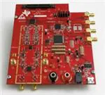
TSW1265EVM Evaluation Module
The TSW1265EVM evaluation module is a wideband, dual-receiver reference design and evaluation
platform. The signal chain allows conversion from RF to bits using a dual-channel downconversion mixer,
the LMH6521 dual-channel, digitally controlled variable gain amplifier (DVGA), and the ADS4249 14-bit
250-MSPS analog-to-digital converter (ADC). The TSW1265EVM also includes the LMK04800 dual-PLL
clock jitter cleaner and generator to provide an onboard low-noise clocking solution. A provided software
GUI allows for configuration of the ADS4249 and LMK04800. Either the GUI or an FPGA using the highspeed connector can control the gain of the LMH6521 DVGA. The EVM mates with the TSW1400 pattern
capture and generation card to capture data from the ADS4249. Then, the High Speed Data Converter
Pro software tool can perform signal analysis. The TSW1265EVM product folder on the TI web site
contains the EVM schematic, bill of materials, and layout files.
1
2
3
Contents
Introduction .................................................................................................................. 2
1.1
Overview ............................................................................................................ 2
1.2
Block Diagram ...................................................................................................... 2
Software Control ............................................................................................................ 3
2.1
Installation Instructions ............................................................................................ 3
2.2
Software Operation ................................................................................................ 3
Basic Test Procedure ....................................................................................................... 9
3.1
TSW1400 Setup .................................................................................................... 9
3.2
Test Setup Block Diagram ...................................................................................... 10
3.3
Quick-Start Procedure ........................................................................................... 10
3.4
Optional Features and Configurations ......................................................................... 12
List of Figures
1
TSW1265EVM Block Diagram ............................................................................................
2
2
ADS4249 Control Tab ......................................................................................................
4
3
LMK04800 Main Tab .......................................................................................................
5
4
LMK04800 Outputs Tab ....................................................................................................
6
5
LMK04800 Advanced Tab .................................................................................................
7
6
LMH6521 Gain Tab .........................................................................................................
8
7
Send All, Save, Load, and Read All ......................................................................................
9
8
Test Setup Block Diagram
...............................................................................................
10
9
TSW1265 Sample Capture using the TSW1400 ......................................................................
11
List of Tables
............................................................................
1
ADS4249 Control Tab Section Descriptions
2
LMK04800 Main Tab Section Descriptions ..............................................................................
5
3
LMK04800 Outputs Tab Section Descriptions ..........................................................................
6
4
LMK04800 Advanced Tab Section Descriptions ........................................................................
7
5
LMH6521 Gain Tab Section Descriptions
...............................................................................
Send All, Save, Load, and Read All Descriptions ......................................................................
8
6
4
9
Windows is a registered trademark of Microsoft Corporation.
All other trademarks are the property of their respective owners.
SLAU429 – March 2012
Submit Documentation Feedback
TSW1265EVM Evaluation Module
Copyright © 2012, Texas Instruments Incorporated
1
�Introduction
www.ti.com
1
Introduction
1.1
Overview
The TSW1265EVM evaluation module is a wideband, dual-receiver reference design and evaluation
platform. The signal chain allows conversion from RF to bits using a dual-channel downconversion mixer,
the LMH6521 dual-channel DVGA, and the ADS4249 14-bit, 250-MSPS ADC. The TSW1265EVM also
includes the LMK04800 dual-PLL clock jitter cleaner and generator to provide an onboard low-noise
clocking solution.
The default configuration of the board allows for an RF frequency of 1700 MHz to 2200 MHz and an LO
frequency of 1750 MHz to 2700 MHz. The IF portion of the board, starting at the output of the mixer to the
ADC input, is set for a center frequency of 187.5 MHz and a 1-dB bandwidth of 75 MHz. Modification of
both the RF and IF frequency ranges is possible and is discussed later.
A software GUI allows for configuring the ADS4249 and LMK04800. The GUI, or alternatively through the
high-speed connector with an FPGA, can control the gain of the LMH6521 DVGA. The EVM mates with
the TSW1400 pattern capture and generation board to capture data from the ADS4249. The High Speed
Data Converter Pro software tool then can perform signal analysis. The TSW1400 and High Speed Data
Converter Pro greatly simplify the evaluation process by providing the hardware and software necessary
for pattern capture and analysis.
1.2
Block Diagram
Figure 1 shows the block diagram of the TSW1265EVM.
6VDC
CLK/REF
IN
CLK/REF
OUT
SMA
SMA
LDO’s
Crystal
Clock
Jitter Cleaner
LMK04800 & Generator
RFIN-A SMA
Downconversion
Mixer
ADS4249
LMH6521
7
LO IN SMA
7
RFIN-B SMA
Data
& Control
Connector
8
SPI
USB/CPLD
8
USB
Conn
Figure 1. TSW1265EVM Block Diagram
2
TSW1265EVM Evaluation Module
SLAU429 – March 2012
Submit Documentation Feedback
Copyright © 2012, Texas Instruments Incorporated
�Software Control
www.ti.com
2
Software Control
This section provides installation instructions and explanations of the TSW1265 GUI.
2.1
Installation Instructions
1. The software can be downloaded from the TSW1265EVM production page on www.ti.com. Find the
page by searching for TSW1265EVM. The software appears under the Related Products section on
the TI Software tab.
2. Extract the files from the zip file named TSW1265 GUI vXpY Installer.zip where XpY represents the
version number.
3. Run setup.exe, and follow the installation prompts.
4. Start the GUI by going to the Start Menu → All Programs → Texas Instruments ADCs → TSW1265
GUI.
5. When plugging the board into the computer for the first time through the USB cable, you are prompted
to install the USB drivers.
• Windows® XP: If Windows XP does not automatically install the drivers, follow the prompts on the
screen to do so. Do not let Windows XP search Microsoft Update for the drivers, but do let
Windows XP install the drivers automatically.
• Windows 7: After installing the TSW1265 GUI, Windows 7 should automatically be able to install
the drivers for the TSW1265EVM with no input from the user.
2.2
Software Operation
The TSW1265 GUI allows the user to program the ADS4249, LMH6521, and LMK04800 for proper
operation. The controls for each device are split between different tabs for a simplified interface. Detailed
descriptions for each tab are below.
SLAU429 – March 2012
Submit Documentation Feedback
TSW1265EVM Evaluation Module
Copyright © 2012, Texas Instruments Incorporated
3
�Software Control
2.2.1
www.ti.com
ADS4249 Control Tab
Figure 2. ADS4249 Control Tab
Table 1. ADS4249 Control Tab Section Descriptions
4
Section
Description
Reset/Readout
Controls the reset and readout functions. Note that readout is not currently functional.
Powerdown Modes
Put the device into either global or standby powerdown modes to lower power
consumption.
Digital Functions
Enable or disable the digital gain functions and set the gain value. Also enables use of
test patterns and offset correction.
Performance Modes
Set the various performance modes
Data and Clock Outputs
Change parameters of the digital and clock outputs such as levels, data format, and
output buffer type.
Test Patterns
Set the test patterns of both channels for testing and troubleshooting of the digital
interface.
Offset Correction
Enable and set parameters of the offset correction feature.
TSW1265EVM Evaluation Module
SLAU429 – March 2012
Submit Documentation Feedback
Copyright © 2012, Texas Instruments Incorporated
�Software Control
www.ti.com
2.2.2
LMK04800 Main Tab
Figure 3. LMK04800 Main Tab
Table 2. LMK04800 Main Tab Section Descriptions
Section
Description
Power Down, Reset, Mode Select
Allows for powering down and resetting the part. Also controls the mode of the
LMK04800.
CLKin Settings
Enabled and select the input clock source, input buffer types, and dividers.
VCO Divider
Set the VCO divider to reduce the frequency on the clock distribution path. It is
recommended to use the VCO directly.
OSCout
Control power to the OSCin port. Also enable and change parameters of the OSCout
pins.
PLL 1 Settings
Configure PLL 1 settings when using the dual PLL mode.
PLL 2 Settings
Configure PLL 2 settings for both dual and single PLL mode.
SLAU429 – March 2012
Submit Documentation Feedback
TSW1265EVM Evaluation Module
Copyright © 2012, Texas Instruments Incorporated
5
�Software Control
2.2.3
www.ti.com
LMK04800 Outputs Tab
Figure 4. LMK04800 Outputs Tab
Table 3. LMK04800 Outputs Tab Section Descriptions
6
Section
Description
Clock Out 0 and 1
Configure Clock Out 0 and 1 outputs. Enable the outputs and set the divider, delay,
and output buffer.
Clock Out 2 and 3
Configure Clock Out 2 and 3 outputs. Enable the outputs and set the divider, delay,
and output buffer.
Clock Out 4 and 5
Configure Clock Out 4 and 5 outputs. Enable the outputs and set the divider, delay,
and output buffer.
Clock Out 6 and 7
Configure Clock Out 6 and 7 outputs. Enable the outputs and set the divider, delay,
and output buffer. Also select the source for the output.
Clock Out 8 and 9
Configure Clock Out 8 and 9 outputs. Enable the outputs and set the divider, delay,
and output buffer. Also select the source for the output.
Clock Out 10 and 11
Configure Clock Out 10 and 11 outputs. Enable the outputs and set the divider, delay,
and output buffer.
TSW1265EVM Evaluation Module
SLAU429 – March 2012
Submit Documentation Feedback
Copyright © 2012, Texas Instruments Incorporated
�Software Control
www.ti.com
2.2.4
LMK04800 Advanced Tab
Figure 5. LMK04800 Advanced Tab
Table 4. LMK04800 Advanced Tab Section Descriptions
Section
Description
SYNC
Enable and configure the sync functionality.
DAC Vtune Rail Detection
Enable and control the internal DAC settings.
Status Pins Setup
Setup the status pins for various outputs as well as control some miscellaneous
functions.
Holdover Mode
Enable and configure holdover mode.
SLAU429 – March 2012
Submit Documentation Feedback
TSW1265EVM Evaluation Module
Copyright © 2012, Texas Instruments Incorporated
7
�Software Control
2.2.5
www.ti.com
LMH6521 Gain Tab
Figure 6. LMH6521 Gain Tab
Table 5. LMH6521 Gain Tab Section Descriptions
8
Section
Description
Channel A
Set the gain for channel A of the LMH6521.
Channel B
Set the gain for channel B of the LMH6521.
TSW1265EVM Evaluation Module
SLAU429 – March 2012
Submit Documentation Feedback
Copyright © 2012, Texas Instruments Incorporated
�Basic Test Procedure
www.ti.com
2.2.6
Send All, Save, Load, Read All
Figure 7. Send All, Save, Load, and Read All
Table 6. Send All, Save, Load, and Read All Descriptions
2.2.7
Section
Description
Send All
Click to send all the registers for all devices. Press a few times if the board does not
seem to be responding correctly.
Save
Save the register settings in a text file. Can be reloaded later to set the GUI and
devices to a known state.
Load
Load a saved configuration.
Read All
This function is not currently enabled on the TSW1265 GUI.
USB Status
The indicator shows the status of the USB connection. The indicator is lit when the USB connection is
valid. If the computer is not connected to the board, click the Reset USB button.
2.2.8
Exit
Click to exit the GUI. Note that the X in the upper right corner of the window has been disabled to ensure
that the USB connection is closed properly.
3
Basic Test Procedure
3.1
TSW1400 Setup
See the TSW1400 User's Guide (SLWU079) for a more detailed explanation of the TSW1400 setup and
its features. This document assumes that the High Speed Data Converter Pro software and the TSW1400
pattern capture and generation board are both installed and functioning properly. This information can be
found at http://www.ti.com/tool/tsw1400evm.
SLAU429 – March 2012
Submit Documentation Feedback
TSW1265EVM Evaluation Module
Copyright © 2012, Texas Instruments Incorporated
9
�Basic Test Procedure
3.2
www.ti.com
Test Setup Block Diagram
Below is a block diagram of the test setup.
PC
USB
USB
5V
Clock Source
(optional)
USB
5V in
CLKIN1
J1
TSW1265
ADC INTERFACE
TSW1400
USB
RFIN-A
REF In
RF Source
REF In
LO2
6V in
6V
LO Source
REF Out
Figure 8. Test Setup Block Diagram
3.3
Quick-Start Procedure
3.3.1
TSW1400 Data Capture Card
1. Connect a 5-V power supply to connector J12 of the TSW1400. Flip switch SW7 to the "ON" position.
2. Insert a USB cable into the USB port on the TSW1400. Connect the other end to the PC.
3.3.2
TSW1265EVM
1. Connect a 6-V power supply to either the banana jacks or the barrel connector. If using the banana
jacks, connect the positive end to J17 and the negative end to J16.
2. Connect a USB cable between the TSW1265 board and the PC.
3. Connect an LO source to the SMA connector labeled LO2. Set the LO source to 1960 MHz and 0
dBm.
4. Connect an RF source to the SMA connector labeled RFIN-B. Because the DVGA may come up with
an unknown gain, set the amplitude of the RF input to -30 dBm to prevent overdriving the ADC on
start-up. Set the frequency to 1780 MHz.
5. Connect the TSW1265 to the TSW1400 by connecting J1 on the TSW1265 to the ADC Interface
connector on the bottom of the TSW1400.
3.3.3
TSW1265 GUI
1. Start the TSW1265 GUI by going to Start Menu → All Programs → Texas Instruments ADCs →
TSW1265 GUI.
2. Make sure the green indicator is lit up indicating that the TSW1265 board has been successfully
connected to the PC. If not, click the "Reset USB" button. If it still is not lit up, check the USB
connection. If the USB connection is correct, unplug the USB cable, wait five seconds and then plug it
back in. Repeat these steps if necessary.
3. Click the "Load" button and select the file named "250MHz_onboard_clock.txt". Click "Ok". The file is
10
TSW1265EVM Evaluation Module
SLAU429 – March 2012
Submit Documentation Feedback
Copyright © 2012, Texas Instruments Incorporated
�Basic Test Procedure
www.ti.com
located in the TSW1265 GUI installation directory in the folder named "Configuration Files".
4. Click "Send All". At this point, the LED labeled "D1" on the TSW1265 should be lit indicating a PLL
lock. If it is not lit, click "Send All" again.
3.3.4
1.
2.
3.
4.
5.
6.
7.
High Speed Data Converter Pro
Start the High Speed Data Convert Pro software tool by going to Start Menu → All Programs → Texas
Instruments ADCs → High Speed Data Converter Pro.
When it prompts for the serial number of the board, select the serial number that represents the
TSW1400 that has been connected to the TSW1265. This number should be on a sticker on the
TSW1400.
In the "Select ADC" drop-down box select "ADS4249". If it asks to download the firmware select "Yes".
Multiple LEDs will light up on the TSW1400 once the firmware has finished downloading.
Select Single Tone from the Test Selection drop-down menu.
At the bottom left corner, enter 250M into the ADC Sampling Rate (Fs) box. Enter 180M into the ADC
Input Target Frequency box. Press the Enter key.
Select Blackman from the drop-down box originally labeled "Rectangular". This applies a Blackman
windowing function because the clock source is not synchronized to the LO and RF sources and
therefore the captured data will not be coherent.
All boards and software are now set up. Click the Capture button. Once the capture is complete, adjust
the input source amplitude and LMH6521 gain as needed to achieve approximately -1 dBFS. The
LMH6521 gain can be changed on the LMH6521 Gain tab of the TSW1265 GUI. An example of a -1dBFS plot is shown in the figure below.
Figure 9. TSW1265 Sample Capture using the TSW1400
SLAU429 – March 2012
Submit Documentation Feedback
TSW1265EVM Evaluation Module
Copyright © 2012, Texas Instruments Incorporated
11
�Basic Test Procedure
3.4
3.4.1
www.ti.com
Optional Features and Configurations
Clocking
The TSW1265EVM allows for multiple clocking configurations by using the LMK04800 clock jitter cleaner
and generation chip. The board comes preinstalled with a 20-MHz crystal which can be used to generate
the sampling clock. The default for the board is a 250-MHz sampling clock.
Since the board is initially setup for a 250-MHz sampling clock, an LC resonant tank filter centered at 250
MHz has been placed on the clock lines to provide filtering of wideband noise. The filter has a wide
enough bandwidth to allow the use of an external 245.76-MHz clock as well. If another clocking frequency
is needed, the LC resonant tank will need to be changed. It can also be removed altogether, but at the
cost of some added clock jitter. Use Equation 1 below to calculate the inductor and capacitor values for
the desired clock frequency. Fc is the center frequency of the filter and Q can be chosen to be an arbitrary
value of 25. Assume R is equal to 100 Ω. Note that the traces from the LMK04800 to the ADC add
approximately 50 pF of capacitance which has already been considered in Equation 1.
L=
1
2pf
Q
R
2
æQö
C = L ç ÷ - 50pF
èRø
(1)
The TSW1265 board comes preinstalled with the LMK04803 which has an internal VCO frequency range
of 1840 MHz to 2030 MHz. If the desired clock cannot be derived from this frequency range using integer
dividers, then this device can be swapped out for another LMK04800 with a different VCO range. Consult
the LMK04800 datasheet (SNAS489H) to determine which LMK04800 will provide the correct VCO range
for the needed clocking frequency.
The LMK04800 can be setup in clock distribution mode or as a clock generator using single or dual PLL
mode. The different modes of operation are discussed below.
• External Clock Mode: The LMK04800 can be setup in clock distribution mode to allow the use of an
external clock source. This can be used for coherent sampling by provided a clock that is synchronized
to the RF and LO signal sources. The TSW1265 GUI includes a configuration file for the external clock
mode. This file is located in the TSW1265 GUI installation directory in the folder "Configuration Files"
and is named "external_clock.txt". The file can be loaded by clicking the "Load" button, navigating to
the correct folder, selecting the file, and clicking "Ok". Click "Send All" a few times to make sure the
board is configured properly. The user provides an external clock through the "CLKIN1" SMA
connector on the TSW1265 board.
• Onboard Clock using Single PLL Mode: This is the default mode of operation for the TSW1265. In
this mode, the 20-MHz crystal is used to generate other frequencies by using the single PLL mode of
the LMK04800. The 20-MHz crystal acts as the reference for the PLL and the divided down internal
VCO acts as the clock source. There is an included configuration file that will setup the LMK04800 in
single PLL mode and generate a 250-MHz sampling clock for the ADS4249. This file is located in the
TSW1265 GUI installation directory in the folder "Configuration Files" and is named
250MHz_onboard_clock.txt. The file can be loaded by clicking the Load button, navigating to the
correct folder, selecting the file, and clicking Ok. Click Send All a few times to make sure the board is
configured properly. The LED labeled D1 on the board will light up indicating that the PLL is locked.
• Onboard Clock using Dual PLL Mode: This mode of operation allows the user to provide a low
frequency reference through the CLKIN1 connector to generate a synchronized, higher frequency
sampling clock. The reference can come from any source, such as a 10-MHz reference from a piece of
test equipment. This allows for synchronization between all signal sources and for coherent sampling.
In order to use this mode, a VCXO needs to be installed at Y2 or Y4. Additionally, R69, R66, C168,
C167 should be removed and install 50 Ω for R97, 0.1 uF for C73, and 0.1 uF for C167. The user must
update the loop filters if a change in the reference or VCXO occurs. Use the Clock Design Tool
(http://www.ti.com/tool/clockdesigntool) to design the loop filters and PLL settings based on the
reference, VCXO, and output frequencies.
12
TSW1265EVM Evaluation Module
SLAU429 – March 2012
Submit Documentation Feedback
Copyright © 2012, Texas Instruments Incorporated
�Basic Test Procedure
www.ti.com
3.4.2
Changing the RF and LO Frequencies
The default RF frequency range is 1700 MHz to 2200 MHz. The default LO frequency range is 1750 MHz
to 2700 MHz. These ranges are set by the MAX19995A downconversion mixer. The board was designed
to work with most of the Maxim and Skyworks downconversion mixers, therefore the mixer can be
replaced with a different one that has different frequency ranges. The passive components will also need
to be changed based on the data sheet of the part.
3.4.3
Changing the IF Frequency
The IF frequency of the TSW1265 is fixed due to the LC filters on the board. There is a filter between the
mixer and the LMH6521 and a filter between the LMH6521 and the ADS4249. These filters provide an
overall 1-dB bandwidth of 75 MHz centered at 187.5 MHz. The filter between the mixer and the LMH6521
is a second-order LC filter with a 1-dB bandwidth of approximately 140 MHz. The filter between the
LMH6521 and the ADS4249 is a fourth order with a bandwidth of 75 MHz.
To change the IF frequency of the TSW1265, the user needs to change the filters that are implemented on
the board. There are many tools available for download online that will calculate a filter design based on
frequency and ripple requirements. Use these tools to get a starting point for the filter design. Due to
parasitic capacitance and inductance on the board, the user must interactively tune the filter to achieve the
desired response. Once the filter has been designed for one channel, it can be implemented on the other
channel as well. Note that the transformer following the IF filter is in place to correct for any imbalances
between the two legs of the differential signal. For more detailed information about how to design the IF
filters see the application note titled "Band-Pass Filter Design Techniques for High-Speed ADCs"
(SBAA195).
3.4.4
Using the High-Speed Connector to Set the DVGA Gain
The high-speed connector (J1) on the TSW1265 board has connections that allow a user to change the
gain of the LMH6521 quickly. Pins 105, 107, 109, 111, 113, 115, 117, and 119 on the connector can be
used to pass the gain and latch signals from an FPGA to the DVGA. To use this feature, the jumper JP9
needs to be moved between pins 2 and 3. This configures the CPLD to route the gain from the connector
rather than from the USB connection.
SLAU429 – March 2012
Submit Documentation Feedback
TSW1265EVM Evaluation Module
Copyright © 2012, Texas Instruments Incorporated
13
�EVALUATION BOARD/KIT/MODULE (EVM) ADDITIONAL TERMS
Texas Instruments (TI) provides the enclosed Evaluation Board/Kit/Module (EVM) under the following conditions:
The user assumes all responsibility and liability for proper and safe handling of the goods. Further, the user indemnifies TI from all claims
arising from the handling or use of the goods.
Should this evaluation board/kit not meet the specifications indicated in the User’s Guide, the board/kit may be returned within 30 days from
the date of delivery for a full refund. THE FOREGOING LIMITED WARRANTY IS THE EXCLUSIVE WARRANTY MADE BY SELLER TO
BUYER AND IS IN LIEU OF ALL OTHER WARRANTIES, EXPRESSED, IMPLIED, OR STATUTORY, INCLUDING ANY WARRANTY OF
MERCHANTABILITY OR FITNESS FOR ANY PARTICULAR PURPOSE. EXCEPT TO THE EXTENT OF THE INDEMNITY SET FORTH
ABOVE, NEITHER PARTY SHALL BE LIABLE TO THE OTHER FOR ANY INDIRECT, SPECIAL, INCIDENTAL, OR CONSEQUENTIAL
DAMAGES.
Please read the User's Guide and, specifically, the Warnings and Restrictions notice in the User's Guide prior to handling the product. This
notice contains important safety information about temperatures and voltages. For additional information on TI's environmental and/or safety
programs, please visit www.ti.com/esh or contact TI.
No license is granted under any patent right or other intellectual property right of TI covering or relating to any machine, process, or
combination in which such TI products or services might be or are used. TI currently deals with a variety of customers for products, and
therefore our arrangement with the user is not exclusive. TI assumes no liability for applications assistance, customer product design,
software performance, or infringement of patents or services described herein.
REGULATORY COMPLIANCE INFORMATION
As noted in the EVM User’s Guide and/or EVM itself, this EVM and/or accompanying hardware may or may not be subject to the Federal
Communications Commission (FCC) and Industry Canada (IC) rules.
For EVMs not subject to the above rules, this evaluation board/kit/module is intended for use for ENGINEERING DEVELOPMENT,
DEMONSTRATION OR EVALUATION PURPOSES ONLY and is not considered by TI to be a finished end product fit for general consumer
use. It generates, uses, and can radiate radio frequency energy and has not been tested for compliance with the limits of computing
devices pursuant to part 15 of FCC or ICES-003 rules, which are designed to provide reasonable protection against radio frequency
interference. Operation of the equipment may cause interference with radio communications, in which case the user at his own expense will
be required to take whatever measures may be required to correct this interference.
General Statement for EVMs including a radio
User Power/Frequency Use Obligations: This radio is intended for development/professional use only in legally allocated frequency and
power limits. Any use of radio frequencies and/or power availability of this EVM and its development application(s) must comply with local
laws governing radio spectrum allocation and power limits for this evaluation module. It is the user’s sole responsibility to only operate this
radio in legally acceptable frequency space and within legally mandated power limitations. Any exceptions to this are strictly prohibited and
unauthorized by Texas Instruments unless user has obtained appropriate experimental/development licenses from local regulatory
authorities, which is responsibility of user including its acceptable authorization.
For EVMs annotated as FCC – FEDERAL COMMUNICATIONS COMMISSION Part 15 Compliant
Caution
This device complies with part 15 of the FCC Rules. Operation is subject to the following two conditions: (1) This device may not cause
harmful interference, and (2) this device must accept any interference received, including interference that may cause undesired operation.
Changes or modifications not expressly approved by the party responsible for compliance could void the user's authority to operate the
equipment.
FCC Interference Statement for Class A EVM devices
This equipment has been tested and found to comply with the limits for a Class A digital device, pursuant to part 15 of the FCC Rules.
These limits are designed to provide reasonable protection against harmful interference when the equipment is operated in a commercial
environment. This equipment generates, uses, and can radiate radio frequency energy and, if not installed and used in accordance with the
instruction manual, may cause harmful interference to radio communications. Operation of this equipment in a residential area is likely to
cause harmful interference in which case the user will be required to correct the interference at his own expense.
�FCC Interference Statement for Class B EVM devices
This equipment has been tested and found to comply with the limits for a Class B digital device, pursuant to part 15 of the FCC Rules.
These limits are designed to provide reasonable protection against harmful interference in a residential installation. This equipment
generates, uses and can radiate radio frequency energy and, if not installed and used in accordance with the instructions, may cause
harmful interference to radio communications. However, there is no guarantee that interference will not occur in a particular installation. If
this equipment does cause harmful interference to radio or television reception, which can be determined by turning the equipment off and
on, the user is encouraged to try to correct the interference by one or more of the following measures:
• Reorient or relocate the receiving antenna.
• Increase the separation between the equipment and receiver.
• Connect the equipment into an outlet on a circuit different from that to which the receiver is connected.
• Consult the dealer or an experienced radio/TV technician for help.
For EVMs annotated as IC – INDUSTRY CANADA Compliant
This Class A or B digital apparatus complies with Canadian ICES-003.
Changes or modifications not expressly approved by the party responsible for compliance could void the user’s authority to operate the
equipment.
Concerning EVMs including radio transmitters
This device complies with Industry Canada licence-exempt RSS standard(s). Operation is subject to the following two conditions: (1) this
device may not cause interference, and (2) this device must accept any interference, including interference that may cause undesired
operation of the device.
Concerning EVMs including detachable antennas
Under Industry Canada regulations, this radio transmitter may only operate using an antenna of a type and maximum (or lesser) gain
approved for the transmitter by Industry Canada. To reduce potential radio interference to other users, the antenna type and its gain should
be so chosen that the equivalent isotropically radiated power (e.i.r.p.) is not more than that necessary for successful communication.
This radio transmitter has been approved by Industry Canada to operate with the antenna types listed in the user guide with the maximum
permissible gain and required antenna impedance for each antenna type indicated. Antenna types not included in this list, having a gain
greater than the maximum gain indicated for that type, are strictly prohibited for use with this device.
Cet appareil numérique de la classe A ou B est conforme à la norme NMB-003 du Canada.
Les changements ou les modifications pas expressément approuvés par la partie responsable de la conformité ont pu vider l’autorité de
l'utilisateur pour actionner l'équipement.
Concernant les EVMs avec appareils radio
Le présent appareil est conforme aux CNR d'Industrie Canada applicables aux appareils radio exempts de licence. L'exploitation est
autorisée aux deux conditions suivantes : (1) l'appareil ne doit pas produire de brouillage, et (2) l'utilisateur de l'appareil doit accepter tout
brouillage radioélectrique subi, même si le brouillage est susceptible d'en compromettre le fonctionnement.
Concernant les EVMs avec antennes détachables
Conformément à la réglementation d'Industrie Canada, le présent émetteur radio peut fonctionner avec une antenne d'un type et d'un gain
maximal (ou inférieur) approuvé pour l'émetteur par Industrie Canada. Dans le but de réduire les risques de brouillage radioélectrique à
l'intention des autres utilisateurs, il faut choisir le type d'antenne et son gain de sorte que la puissance isotrope rayonnée équivalente
(p.i.r.e.) ne dépasse pas l'intensité nécessaire à l'établissement d'une communication satisfaisante.
Le présent émetteur radio a été approuvé par Industrie Canada pour fonctionner avec les types d'antenne énumérés dans le manuel
d’usage et ayant un gain admissible maximal et l'impédance requise pour chaque type d'antenne. Les types d'antenne non inclus dans
cette liste, ou dont le gain est supérieur au gain maximal indiqué, sont strictement interdits pour l'exploitation de l'émetteur.
SPACER
SPACER
SPACER
SPACER
SPACER
SPACER
SPACER
SPACER
�【Important Notice for Users of EVMs for RF Products in Japan】
】
This development kit is NOT certified as Confirming to Technical Regulations of Radio Law of Japan
If you use this product in Japan, you are required by Radio Law of Japan to follow the instructions below with respect to this product:
1.
2.
3.
Use this product in a shielded room or any other test facility as defined in the notification #173 issued by Ministry of Internal Affairs and
Communications on March 28, 2006, based on Sub-section 1.1 of Article 6 of the Ministry’s Rule for Enforcement of Radio Law of
Japan,
Use this product only after you obtained the license of Test Radio Station as provided in Radio Law of Japan with respect to this
product, or
Use of this product only after you obtained the Technical Regulations Conformity Certification as provided in Radio Law of Japan with
respect to this product. Also, please do not transfer this product, unless you give the same notice above to the transferee. Please note
that if you could not follow the instructions above, you will be subject to penalties of Radio Law of Japan.
Texas Instruments Japan Limited
(address) 24-1, Nishi-Shinjuku 6 chome, Shinjuku-ku, Tokyo, Japan
http://www.tij.co.jp
【無線電波を送信する製品の開発キットをお使いになる際の注意事項】
本開発キットは技術基準適合証明を受けておりません。
本製品のご使用に際しては、電波法遵守のため、以下のいずれかの措置を取っていただく必要がありますのでご注意ください。
1.
2.
3.
電波法施行規則第6条第1項第1号に基づく平成18年3月28日総務省告示第173号で定められた電波暗室等の試験設備でご使用いただく。
実験局の免許を取得後ご使用いただく。
技術基準適合証明を取得後ご使用いただく。
なお、本製品は、上記の「ご使用にあたっての注意」を譲渡先、移転先に通知しない限り、譲渡、移転できないものとします。
上記を遵守頂けない場合は、電波法の罰則が適用される可能性があることをご留意ください。
日本テキサス・インスツルメンツ株式会社
東京都新宿区西新宿6丁目24番1号
西新宿三井ビル
http://www.tij.co.jp
SPACER
SPACER
SPACER
SPACER
SPACER
SPACER
SPACER
SPACER
SPACER
SPACER
SPACER
SPACER
SPACER
SPACER
SPACER
SPACER
SPACER
�EVALUATION BOARD/KIT/MODULE (EVM)
WARNINGS, RESTRICTIONS AND DISCLAIMERS
For Feasibility Evaluation Only, in Laboratory/Development Environments. Unless otherwise indicated, this EVM is not a finished
electrical equipment and not intended for consumer use. It is intended solely for use for preliminary feasibility evaluation in
laboratory/development environments by technically qualified electronics experts who are familiar with the dangers and application risks
associated with handling electrical mechanical components, systems and subsystems. It should not be used as all or part of a finished end
product.
Your Sole Responsibility and Risk. You acknowledge, represent and agree that:
1.
2.
3.
4.
You have unique knowledge concerning Federal, State and local regulatory requirements (including but not limited to Food and Drug
Administration regulations, if applicable) which relate to your products and which relate to your use (and/or that of your employees,
affiliates, contractors or designees) of the EVM for evaluation, testing and other purposes.
You have full and exclusive responsibility to assure the safety and compliance of your products with all such laws and other applicable
regulatory requirements, and also to assure the safety of any activities to be conducted by you and/or your employees, affiliates,
contractors or designees, using the EVM. Further, you are responsible to assure that any interfaces (electronic and/or mechanical)
between the EVM and any human body are designed with suitable isolation and means to safely limit accessible leakage currents to
minimize the risk of electrical shock hazard.
Since the EVM is not a completed product, it may not meet all applicable regulatory and safety compliance standards (such as UL,
CSA, VDE, CE, RoHS and WEEE) which may normally be associated with similar items. You assume full responsibility to determine
and/or assure compliance with any such standards and related certifications as may be applicable. You will employ reasonable
safeguards to ensure that your use of the EVM will not result in any property damage, injury or death, even if the EVM should fail to
perform as described or expected.
You will take care of proper disposal and recycling of the EVM’s electronic components and packing materials.
Certain Instructions. It is important to operate this EVM within TI’s recommended specifications and environmental considerations per the
user guidelines. Exceeding the specified EVM ratings (including but not limited to input and output voltage, current, power, and
environmental ranges) may cause property damage, personal injury or death. If there are questions concerning these ratings please contact
a TI field representative prior to connecting interface electronics including input power and intended loads. Any loads applied outside of the
specified output range may result in unintended and/or inaccurate operation and/or possible permanent damage to the EVM and/or
interface electronics. Please consult the EVM User's Guide prior to connecting any load to the EVM output. If there is uncertainty as to the
load specification, please contact a TI field representative. During normal operation, some circuit components may have case temperatures
greater than 60°C as long as the input and output are maintained at a normal ambient operating temperature. These components include
but are not limited to linear regulators, switching transistors, pass transistors, and current sense resistors which can be identified using the
EVM schematic located in the EVM User's Guide. When placing measurement probes near these devices during normal operation, please
be aware that these devices may be very warm to the touch. As with all electronic evaluation tools, only qualified personnel knowledgeable
in electronic measurement and diagnostics normally found in development environments should use these EVMs.
Agreement to Defend, Indemnify and Hold Harmless. You agree to defend, indemnify and hold TI, its licensors and their representatives
harmless from and against any and all claims, damages, losses, expenses, costs and liabilities (collectively, "Claims") arising out of or in
connection with any use of the EVM that is not in accordance with the terms of the agreement. This obligation shall apply whether Claims
arise under law of tort or contract or any other legal theory, and even if the EVM fails to perform as described or expected.
Safety-Critical or Life-Critical Applications. If you intend to evaluate the components for possible use in safety critical applications (such
as life support) where a failure of the TI product would reasonably be expected to cause severe personal injury or death, such as devices
which are classified as FDA Class III or similar classification, then you must specifically notify TI of such intent and enter into a separate
Assurance and Indemnity Agreement.
Mailing Address: Texas Instruments, Post Office Box 655303, Dallas, Texas 75265
Copyright © 2013, Texas Instruments Incorporated
�IMPORTANT NOTICE
Texas Instruments Incorporated and its subsidiaries (TI) reserve the right to make corrections, enhancements, improvements and other
changes to its semiconductor products and services per JESD46, latest issue, and to discontinue any product or service per JESD48, latest
issue. Buyers should obtain the latest relevant information before placing orders and should verify that such information is current and
complete. All semiconductor products (also referred to herein as “components”) are sold subject to TI’s terms and conditions of sale
supplied at the time of order acknowledgment.
TI warrants performance of its components to the specifications applicable at the time of sale, in accordance with the warranty in TI’s terms
and conditions of sale of semiconductor products. Testing and other quality control techniques are used to the extent TI deems necessary
to support this warranty. Except where mandated by applicable law, testing of all parameters of each component is not necessarily
performed.
TI assumes no liability for applications assistance or the design of Buyers’ products. Buyers are responsible for their products and
applications using TI components. To minimize the risks associated with Buyers’ products and applications, Buyers should provide
adequate design and operating safeguards.
TI does not warrant or represent that any license, either express or implied, is granted under any patent right, copyright, mask work right, or
other intellectual property right relating to any combination, machine, or process in which TI components or services are used. Information
published by TI regarding third-party products or services does not constitute a license to use such products or services or a warranty or
endorsement thereof. Use of such information may require a license from a third party under the patents or other intellectual property of the
third party, or a license from TI under the patents or other intellectual property of TI.
Reproduction of significant portions of TI information in TI data books or data sheets is permissible only if reproduction is without alteration
and is accompanied by all associated warranties, conditions, limitations, and notices. TI is not responsible or liable for such altered
documentation. Information of third parties may be subject to additional restrictions.
Resale of TI components or services with statements different from or beyond the parameters stated by TI for that component or service
voids all express and any implied warranties for the associated TI component or service and is an unfair and deceptive business practice.
TI is not responsible or liable for any such statements.
Buyer acknowledges and agrees that it is solely responsible for compliance with all legal, regulatory and safety-related requirements
concerning its products, and any use of TI components in its applications, notwithstanding any applications-related information or support
that may be provided by TI. Buyer represents and agrees that it has all the necessary expertise to create and implement safeguards which
anticipate dangerous consequences of failures, monitor failures and their consequences, lessen the likelihood of failures that might cause
harm and take appropriate remedial actions. Buyer will fully indemnify TI and its representatives against any damages arising out of the use
of any TI components in safety-critical applications.
In some cases, TI components may be promoted specifically to facilitate safety-related applications. With such components, TI’s goal is to
help enable customers to design and create their own end-product solutions that meet applicable functional safety standards and
requirements. Nonetheless, such components are subject to these terms.
No TI components are authorized for use in FDA Class III (or similar life-critical medical equipment) unless authorized officers of the parties
have executed a special agreement specifically governing such use.
Only those TI components which TI has specifically designated as military grade or “enhanced plastic” are designed and intended for use in
military/aerospace applications or environments. Buyer acknowledges and agrees that any military or aerospace use of TI components
which have not been so designated is solely at the Buyer's risk, and that Buyer is solely responsible for compliance with all legal and
regulatory requirements in connection with such use.
TI has specifically designated certain components as meeting ISO/TS16949 requirements, mainly for automotive use. In any case of use of
non-designated products, TI will not be responsible for any failure to meet ISO/TS16949.
Products
Applications
Audio
www.ti.com/audio
Automotive and Transportation
www.ti.com/automotive
Amplifiers
amplifier.ti.com
Communications and Telecom
www.ti.com/communications
Data Converters
dataconverter.ti.com
Computers and Peripherals
www.ti.com/computers
DLP® Products
www.dlp.com
Consumer Electronics
www.ti.com/consumer-apps
DSP
dsp.ti.com
Energy and Lighting
www.ti.com/energy
Clocks and Timers
www.ti.com/clocks
Industrial
www.ti.com/industrial
Interface
interface.ti.com
Medical
www.ti.com/medical
Logic
logic.ti.com
Security
www.ti.com/security
Power Mgmt
power.ti.com
Space, Avionics and Defense
www.ti.com/space-avionics-defense
Microcontrollers
microcontroller.ti.com
Video and Imaging
www.ti.com/video
RFID
www.ti-rfid.com
OMAP Applications Processors
www.ti.com/omap
TI E2E Community
e2e.ti.com
Wireless Connectivity
www.ti.com/wirelessconnectivity
Mailing Address: Texas Instruments, Post Office Box 655303, Dallas, Texas 75265
Copyright © 2013, Texas Instruments Incorporated
�