Product
Folder
Order
Now
Technical
Documents
Support &
Community
Tools &
Software
TUSB422
SLLSEW6C – NOVEMBER 2016 – REVISED JUNE 2018
TUSB422 USB Type-C™ Port Control with Power Delivery
1 Features
3 Description
•
TUSB422 is a USB PD PHY that enables a USB
Type-C port with the Configuration Channel (CC)
logic needed for USB Type-C ecosystems. It
integrates the physical layer of the USB BMC power
delivery (PD) protocol to allow up to 100-W of power
and support for alternate mode interfaces. An
external microprocessor, containing USB Type-C Port
Manager (TCPM), communicates with the TUSB422
through an I2C interface.
1
•
•
•
•
•
•
•
•
•
Supports USB Type-C™ 1.2 and Power Delivery
(PD) Specifications
USB PD Phy with I2C Interface (TCPCi)
Supporting:
– 5 — 24 V Power Sourcing and Sinking
– 2.5 Watt VCONN switch
– Alt Mode Negotiations
Optimized for Portable Applications with
Autonomous Dual Role Port (DRP) Support
Software Configurable as Dedicated Host,
Dedicated Device, or Dual-Role
– DFP, UFP and DRP
– Attach/Detach of USB port
– Cable Orientation Detection
– Current Mode Advertisement and Detection
– Debug and Audio Accessory Support
– Active Cable Detection
– VCONN for Active Cable
Dead Battery Support
Integrated over-temperature sensing diode
(OTSD)
VBUS Detect and Discharge Control
VDD Supply Voltage: 2.7 V — 5.5 V
Low Current Consumption
Industrial Temperature Range of –40°C to 85°C
The TUSB422 integrates 2.5 Watt switch to provide
VCONN power for an active cable. The device also
provides VCONN discharge function. The TUSB422
also supports USB Type-C optional features such as
audio and debug accessory.
The device operates over a wide supply-range and
has low power consumption. The TUSB422 is
available in industrial temperature ranges.
Device Information(1)
PART NUMBER
TUSB422
PACKAGE
BODY SIZE (NOM)
1.335mm x 1.380mm at
0.4mm pitch
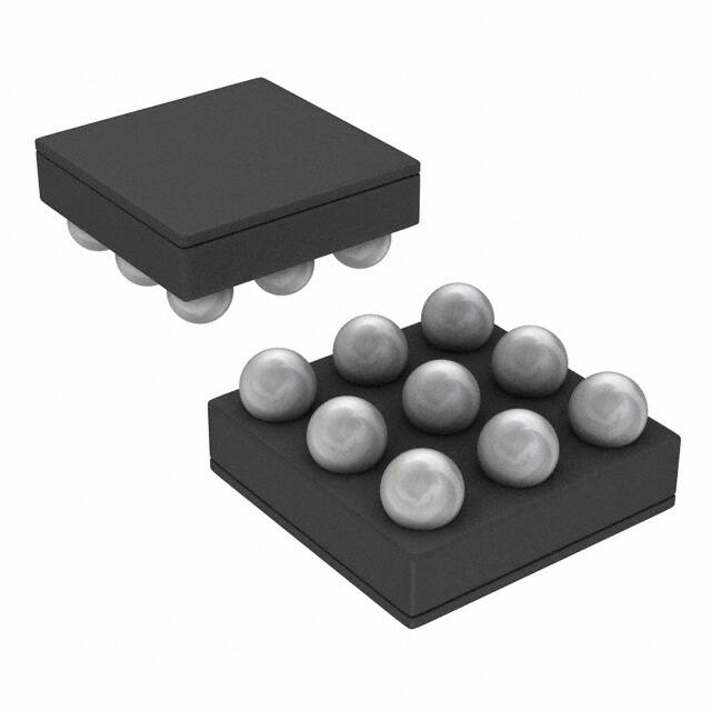
WCSP (9)
(1) For all available packages, see the orderable addendum at
the end of the data sheet.
2 Applications
•
•
•
Under control of the TCPM, TUSB422 uses the CC
pins to determine port attach/detach, cable
orientation, role detection, and port control for USB
Type-C current mode. The TUSB422 can be
configured as DFP, UFP, or DRP, depending on the
application. The TUSB422 implements VBUS
detection and discharge for the implementation of a
compliant USB Type-C port.
Smartphones
Tablets, Notebooks, Desktops
Wall Charger, Power Banks
SPACER
Simplified Schematic
VDD
VBUS_DET
VBUS
Detection &
Discharge
I2C
Slave
TCPC
INT
USB Type-C Smartphone
VCONN
VCONN
Switch
Type-C
Channel
Configuration
CC1
CC2
SCL
Config
Control
SDA
GND
APU
USB PD Phy
USB Type-C
Port Manager
TUSB422
USB Typ-C
Port Controller
USB Type-C
1
An IMPORTANT NOTICE at the end of this data sheet addresses availability, warranty, changes, use in safety-critical applications,
intellectual property matters and other important disclaimers. PRODUCTION DATA.
�TUSB422
SLLSEW6C – NOVEMBER 2016 – REVISED JUNE 2018
www.ti.com
Table of Contents
1
2
3
4
5
6
Features ..................................................................
Applications ...........................................................
Description .............................................................
Revision History.....................................................
Pin Configuration and Functions .........................
Specifications.........................................................
6.1
6.2
6.3
6.4
6.5
6.6
6.7
7
1
1
1
2
3
4
Absolute Maximum Ratings ...................................... 4
ESD Ratings.............................................................. 4
Recommended Operating Conditions....................... 4
Thermal Information .................................................. 5
Electrical Characteristics........................................... 5
Timing Requirements ................................................ 8
Typical Characteristics ............................................ 10
Detailed Description ............................................ 11
7.1 Overview ................................................................. 11
7.2 Functional Block Diagram ....................................... 11
7.3 Feature Description................................................. 12
7.4 Device Functional Modes........................................ 17
7.5 Programming........................................................... 19
7.6 Register Maps ......................................................... 22
8
Application and Implementation ........................ 63
8.1 Application Information............................................ 63
8.2 Typical Application ................................................. 63
9 Power Supply Recommendations...................... 65
10 Layout................................................................... 66
10.1 Layout Guidelines ................................................. 66
10.2 Layout Example .................................................... 66
11 Device and Documentation Support ................. 67
11.1
11.2
11.3
11.4
11.5
Receiving Notification of Documentation Updates
Community Resources..........................................
Trademarks ...........................................................
Electrostatic Discharge Caution ............................
Glossary ................................................................
67
67
67
67
67
12 Mechanical, Packaging, and Orderable
Information ........................................................... 67
4 Revision History
Changes from Revision B (August 2017) to Revision C
Page
•
Changed the VCONN pin description in the Pin Functions table ........................................................................................... 3
•
Deleted VRX(FRS_PD) from electrical characteristics .................................................................................................................. 6
•
Deleted tFRSWAPRX from timing requirements section............................................................................................................... 8
•
Added NOTE: "The TUSB422 supports all PD2.0 and PD 3.0..." to the USB PD BMC PHY section ................................. 12
•
Deleted text from the first paragraph of the Fast Role Swap secton. ................................................................................. 16
•
From: Once VBUS is at VSafe0V, change .. To: Once VBUS is at VSafe0V, disable
AUTO_DISCHARGE_DISCONNECT in Power Control Register and change .. ................................................................ 17
•
From: Once VBUS is at vSafe5V, the TCPM should then send PS_RDY to its port partner. To: Once VBUS is at
vSafe5V, the TCPM should update message header information and then send PS_RDY to its port partner. ................. 17
•
Added NOTE: "During Power-role swap, the TUSB422..." to the Power Role Swap section. ............................................. 18
•
Added NOTE: "When exiting dead battery mode..." to the Dead Battery Mode section...................................................... 18
•
Changed bit 0 From: VCONN_OC_FAULT To Reserved in Figure 31 and Table 28.......................................................... 37
•
Added text: "VBUS present status may be invalid..." to the Bit 2 VBUS_PRESENT description in Table 31 ..................... 40
•
Added text: "Before attempting to transmit..." to the Transmit Register (address = 0x50) [reset = 0x00] register .............. 51
•
Changed bit 0 From: FAST_ROLE_SWAP_STAT To Reserved in Figure 65 and Table 62............................................... 56
•
Changed bit 0 From: FAST_ROLE_SWAP_MASK To Reserved in Figure 66 and Table 63.............................................. 57
•
Changed bit 3 From: FASTROLE_RX_EN To Reserved in Figure 69 and Table 66........................................................... 59
Changes from Revision A (April 2017) to Revision B
•
Changed Bit TX_BUFF_OBJx_BYTE_x From: Read Only To Read/Write in Figure 54 and Table 51 ............................... 52
Changes from Original (November 2016) to Revision A
•
2
Page
Page
Deleted text: "Following sentence optional..." from the ESD Ratings table notes.................................................................. 4
Submit Documentation Feedback
Copyright © 2016–2018, Texas Instruments Incorporated
Product Folder Links: TUSB422
�TUSB422
www.ti.com
SLLSEW6C – NOVEMBER 2016 – REVISED JUNE 2018
5 Pin Configuration and Functions
YFF Package
9 Pin (DSBGA)
Top View
1
2
3
A
CC2
VBUSIN
VDD
B
VCONN
INT_N
SCL
C
CC1
GND
SDA
Not to scale
Pin Functions
PIN
I/O
DESCRIPTION
I/O (FS)
Type-C Configuration channel signal 2. Used for connector orientation, connection detection
and removal, current capabilities, and PD communication. This pin requires an external
CRX(SHUNT) capacitor.
NO.
NAME
A1
CC2
A2
VBUSIN
I
5-24 V VBUS input voltage. Tie directly to VBUS at Type-C connector.
A3
VDD
P
2.7 V to 5.5 V Positive supply voltage
B1
VCONN
P
2.7 V to 5.5 V VCONN. VCONN voltage should be at a valid stable value before software
closes the VCONN switch. If VCONN support is not required in the system, then this pin can
be left floating.
B2
INT_N
B3
SCL
I/O Opendrain (FS)
C1
CC1
I/O (FS)
C2
GND
G
SDA
I/O Opendrain (FS)
C3
O (FS)
Open drain output. Asserted low to indicate status change occurred. Requires an external
pull-up resistor.
SCL - I2C communication clock signal. Requires an external pull-up resistor.
Type-C Configuration channel signal 1. Used for connector orientation, connection detection
and removal, current capabilities, and PD communication. This pin requires an external
CRX(SHUNT) capacitor.
Ground
SDA - I2C communication data signal. Requires an external pull-up resistor.
Submit Documentation Feedback
Copyright © 2016–2018, Texas Instruments Incorporated
Product Folder Links: TUSB422
3
�TUSB422
SLLSEW6C – NOVEMBER 2016 – REVISED JUNE 2018
www.ti.com
6 Specifications
6.1 Absolute Maximum Ratings
over operating free-air temperature range (unless otherwise noted) (1)
MIN
MAX
UNIT
Supply Voltage
VDD
-0.3
6
V
VCONN Switch
voltage
VCONN
-0.3
6
V
INT_N, SDA, SCL
-0.3
6
V
CC1, CC2
-0.3
6
V
VBUSIN
-0.3
26
V
-65
150
°C
Control pins
Storage temperature, Tstg
(1)
Stresses beyond those listed under Absolute Maximum Ratings may cause permanent damage to the device. These are stress ratings
only, which do not imply functional operation of the device at these or any other conditions beyond those indicated under Recommended
Operating Conditions. Exposure to absolute-maximum-rated conditions for extended periods may affect device reliability.
6.2 ESD Ratings
VALUE
V(ESD)
(1)
(2)
Electrostatic discharge
Human body model (HBM), per
ANSI/ESDA/JEDEC JS-001, all pins (1)
±1500
Charged device model (CDM), per
JEDEC specification JESD22-C101, all
pins (2)
±1500
UNIT
V
JEDEC document JEP155 states that 500-V HBM allows safe manufacturing with a standard ESD control process.
JEDEC document JEP157 states that 250-V CDM allows safe manufacturing with a standard ESD control process.
6.3 Recommended Operating Conditions
over operating free-air temperature range (unless otherwise noted)
MIN
NOM
MAX
VDD
Supply voltage range
2.7
3.7
5.5
V
VCONN
VCONN voltage range
2.7
5
5.5
V
VBUSIN
System VBUS voltage
VI2C_SYS
System I2C voltage range that SDA and
SCL are pulled up to
TA
TJ
4
UNIT
0
5
24
V
1.65
1.8
3.6
V
Operating Free air temperature with
VCONN not supported in the system
-40
25
105
°C
Operating Free air temperature with
VCONN supported in the system
-40
25
85
°C
Junction temperature
-40
125
°C
Submit Documentation Feedback
Copyright © 2016–2018, Texas Instruments Incorporated
Product Folder Links: TUSB422
�TUSB422
www.ti.com
SLLSEW6C – NOVEMBER 2016 – REVISED JUNE 2018
6.4 Thermal Information
TUSB422
THERMAL METRIC (1)
YFF (DSBGA)
UNIT
9 PINS
RΘJA
Junction-to-ambient thermal resistance
114.3
°C/W
RΘJC(top)
RΘJB
Junction-to-case (top) thermal resistance
0.7
°C/W
Junction-to-board thermal resistance
24.9
°C/W
ΨJT
Junction-to-top characterization parameter
0.3
°C/W
ΨJB
Junction-to-board characterization parameter
24.9
°C/W
RΘJC(bot)
Junction-to-case (bottom) thermal resistance
NA
°C/W
(1)
For more information about traditional and new thermal metrics, see the Semiconductor and IC Package Thermal Metrics application
report, SPRA953.
6.5 Electrical Characteristics
over operating free-air temperature range (unless otherwise noted)
PARAMETER
TEST CONDITIONS
MIN
TYP
MAX
UNIT
Power Consumption
UFP Current consumption in
I(UNATTACHED_ Unattached.SNK when port is
unconnected and waiting for
UFP)
connection
I(UNATTACHED_
DRP)
VDD = 3.7V
10
µA
DRP Current consumption while
toggling between Unattached.SNK and
Unattached.SRC when port is
VDD = 3.7V
unconnected and waiting for
connection.
12
µA
VDD = 3.7V
11
µA
VDD = 3.7V
330
µA
VDD = 3.7V;
TX_CARRIER_MODE2_SEL = 1;
5.2
mA
I(UNATTACHED_ DFP Current consumption in
Unattached.SRC when port is
DFP)
unconnected and waiting for
connection
I(ACTIVE_UFP)
UFP Current consumption in
attached.SNK Active Mode. PD
Disabled.
UFP current consumption in
I(ACTIVE_UFP_P attached.SNK with PD enabled and
transmitting continuous BIST Carrier
D)
Mode 2.
CC pins (CC1 and CC2)
VCC(USB_DB)
Voltage on both CC pins when in dead
battery and the attached DFP is
VDD = 0V
presenting default current
advertisement
0.25
1.5
V
VCC(MED_DB)
Voltage on both CC pins when in dead
battery and the attached DFP is
VDD = 0V
presenting medium current (1.5A)
advertisement
0.45
1.5
V
VCC(HIGH_DB)
Voltage on both CC pins when in dead
battery and the attached DFP is
VDD = 0V
presenting high current (3.0A)
advertisement
0.88
2.18
V
R(CC_RD)
Pull-down resistor when in UFP or
DRP mode
VDD = 2.7V to 5.5V
4.6
5.1
5.6
kΩ
R(CC_RA)
Pull-down resistor for active cable
VDD = 2.7V to 5.5V
0.8
1
1.2
kΩ
Leakage current through CC pins
VDD = 0V; VCONN = 0V; CC pin =
5.5V
1.36
mA
0.61
V
ICC(LKG)
Voltage level range for detecting a
V(UFP_CC_USB DFP attach when configured as a UFP
and DFP is advertising default current
)
source capability
0.25
Submit Documentation Feedback
Copyright © 2016–2018, Texas Instruments Incorporated
Product Folder Links: TUSB422
5
�TUSB422
SLLSEW6C – NOVEMBER 2016 – REVISED JUNE 2018
www.ti.com
Electrical Characteristics (continued)
over operating free-air temperature range (unless otherwise noted)
PARAMETER
TEST CONDITIONS
MIN
TYP
MAX
UNIT
Voltage level range for detecting a
V(UFP_CC_MED DFP attach when configured as a UFP
and DFP is advertising medium (1.5A)
)
current source capability
0.7
1.16
V
Voltage level range for detecting a
DFP attach when configured as a UFP
and DFP is advertising high (3.0A)
current source capability
1.31
2.04
V
Voltage threshold for detecting a UFP
attach when TUSB422 is advertising
default current source capability.
1.51
1.6
1.64
V
Voltage threshold for detecting a UFP
VTH(DFP_CC_M attach when TUSB422 is advertising
medium current (1.5A) source
ED)
capability.
1.51
1.6
1.64
V
Voltage threshold for detecting a UFP
attach when TUSB422 is advertising
high current (3.0A) source capability.
2.46
2.6
2.74
V
Voltage threshold for detecting a
active cable attach when advertising
default current
0.15
0.2
0.25
V
Voltage threshold for detecting a
active cable attach when advertising
medium current
0.35
0.4
0.45
V
Voltage threshold for detecting a
active cable attach when advertising
high current.
0.76
0.8
0.84
V
ICC(DEFAULT_P Default mode pull-up current source
when advertising default current.
)
64
80
96
µA
ICC(MED_P)
Medium (1.5A) mode pull-up current
source when advertising medium
current.
166
180
194
µA
ICC(HIGH_P)
High (3.0A) mode pull-up current
source when advertising high current.
VDD > 3.0V
304
330
356
µA
RTX(PD)
Output impedance of CC1/CC2 during
TX when operating in PD mode and
driving the CC line.
At 750KHz
33
48
75
Ω
RTX(FRS_PD)
Fast Role Swap request transmit
driver resistance (excluding cable
resistance)
5
Ω
VOH(PD)
Transmit high voltage when operating
in PD mode
1.2
V
VOL(PD)
Transmit low voltage when operating
in PD mode.
0.07
V
RRX(PD)
Receiver input impedance. Does Not
include pull-up or pulldown resistance
from cable detect.
VIH(PD_SRC)
Input high voltage when sourcing
power. Selected when POWER_ROLE
= 1.
0.8925
1.5325
V
VIH(PD_SNK)
Input high voltage when sinking
power. Selected when POWER_ROLE
= 0.
0.6425
1.5325
V
VIL(PD_SRC)
Input low voltage when sourcing
power. Selected when POWER_ROLE
= 1.
-0.3325
0.4825
V
VIL(PD_SNK)
Input low voltage when sinking power.
Selected when POWER_ROLE = 0.
-0.3325
0.2325
V
V(UFP_CC_HIG
H)
VTH(DFP_CC_U
SB)
VTH(DFP_CC_HI
GH)
VTH(AC_CC_US
B)
VTH(AC_CC_ME
D)
VTH(AC_CC_HI
GH)
6
1.05
TX is Hi-Z
Submit Documentation Feedback
1.125
1
MΩ
Copyright © 2016–2018, Texas Instruments Incorporated
Product Folder Links: TUSB422
�TUSB422
www.ti.com
SLLSEW6C – NOVEMBER 2016 – REVISED JUNE 2018
Electrical Characteristics (continued)
over operating free-air temperature range (unless otherwise noted)
PARAMETER
CRX(SHUNT)
TEST CONDITIONS
External shunt capacitance on both
CC1 and CC2.
MIN
TYP
MAX
UNIT
200
450
pF
-1
1
µA
0.4
V
Control pins: INT_N
I(INTN_LEAK)
INT_N leakage
VDD = 0V; 0 < INT_N < 3.3V
VOL
Low-level signal output voltage
IOL = -2mA
I2C (SDA and SCL). VDD must be above 3V to operate at 3.3V I2C levels
VIH(I2C)
High-level input signal voltage
1.2
V
VIL(I2C)
Low-level input signal voltage
0.4
V
VOL(I2C)
Low-level signal output voltage (opendrain)
0.4
V
IOL(I2C)
Low level output current
I(I2C_LKG)
Leakage through SDA and SCL pins
C(I2C)
Capacitance for SDA and SCL pins
C(I2C_FM+_BUS
6
VDD = 0V; pin pulled up to 3.6V
mA
-1
1
µA
10
pF
I2C bus capacitance for FM+ (1MHz)
150
pF
I2C bus capacitance for FM (400KHz)
150
pF
)
C(I2C_FM_BUS)
R(EXT_I2C_FM+ External resistors on both SDA and
SCL when operating at FM+ (1MHz)
)
R(EXT_I2C_FM)
External resistors on both SDA and
SCL when operating at FM (400KHz)
C(I2C_FM+_BUS) = 150pF
620
820
910
Ω
C(I2C_FM_BUS) = 150pF
620
1500
2200
Ω
0.4
0.75
Ω
5
V
VCONN
RDS(ON)
ON resistance of the VCONN power
FET.
V(PASS)
Voltage to pass through VCONN
power FET
I(VCONN)
VCONN current limit; VCONN is
disconnected above this voltage.
V(VCONN_PRES
Threshold for detecting Vconn present.
500
650
850
mA
2
2.4
V
200
µF
5.6
KΩ
)
C(VCONN)
Bulk capacitance on VCONN; Placed
on VCONN pin supply
10
R(VCONN_DIS)
Resistance to GND when Vconn
discharge is enabled
4.6
C(BULK_SRC)
Source External bulk capacitance
when operating as VBUS Source.
10
150
µF
C(SNK)
Sink External bulk capacitance on
VBUS at connector
1
10
µF
C(SNKPD)
Sink External bulk capacitance on
VBUS after success PD negotiation
1
100
µF
R(BLEED)
Resistance to gnd when bleed
discharge is enabled
8
12.5
KΩ
V(SRCSLEWNE
VBUS discharge maximum slew rate
-30
mV/µs
5.1
VBUSIN
10
G)
V(VBUS_MEASU VBUS_VOLTAGE register
measurement accuracy
RE_ACC)
-2
2
%
OTSD
T(OTSD1)
TJ over temperature trip threshold
resulting in VCONN turn off and flag
set.
150
°C
Submit Documentation Feedback
Copyright © 2016–2018, Texas Instruments Incorporated
Product Folder Links: TUSB422
7
�TUSB422
SLLSEW6C – NOVEMBER 2016 – REVISED JUNE 2018
www.ti.com
6.6 Timing Requirements
MIN
NOM
MAX
UNIT
CC pins in PD mode
Fbr_PD
Bit Rate
270
300
330
Kbps
tUI_PD
Unit Interval
3.03
3.3
3.7
µs
tRISE_PD
Rise time
10% to 90%; CRX(SHUNT) = 200pF
300
ns
tFALL_PD
Fall time
90% to 10%; CRX(SHUNT) = 200pF
300
ns
tRxFilter
Rx Bandwidth limiting filter
100
ns
tInterFrameCap
Time from the end of last bit of a
frame until the state of the first bit of
the next pre-amble
25
50
µs
tStartDrive
Time before the start of the first bit of
the preamble when the transmitter
shall start driving the line.
-1
1
µs
tEndDriveBMC
Time to cease driving the line after the
end of the last bit of a frame
23
µs
tHoldLowBMC
Time to cease driving the line after the
final high-to-low transition
23
µs
nTransitionC
ount
Transitions for signal detect
tFRSWAPTX
Fast Role Swap request transmit
duration
60
120
µs
0.001
1
1
Number of transitions to be detected
to declare bus non-idle
3
I2C (SDA and SCL)
fSCL
SCL clock frequency
tHD;STA
Hold time (repeated) start condition
tLOW
MHz
0.26
µs
Low period of SCL
0.5
µs
tHIGH
High period of SCL
0.26
µs
tSU;STA
Setup time for a repeated start
condition
0.26
µs
tHD;DAT
Data Hold Time
0
µs
tSU;DAT
Data setup time
50
µs
tSU;STOP
Setup time for STOP condition
0.26
µs
tBUF
Bus free time between STOP and
START condition
0.5
µs
tVD;DAT
Data valid time
0.45
µs
tVD;ACK
Data valid acknowledge time
0.45
µs
tR_I2C
Rise time of both SDA and SCL
30% to 70%
120
ns
tF_I2C
Fall time of both SDA and SCL
70% to 30%
120
ns
Delay from Vconn fault detected to
Vconn fault status flag set
20
µs
Delay from Vconn fault detected to
Vconn switch opened
50
ns
4
ms
40
ms
14
VCONN Fault
tVCONN_FAULT
_DLY
tVCONN_OPEN
Power-Up Requirements
tINT_N_LOW
Time from VDD (min) to TUSB422
asserts INT_N low.
Measured from VDD(min) to INT_N
pin at VOL(min).
tVDD_RISE
VDD rise time
Measured from 0V to VDD(min)
Sampling timings
tCC_SAMPLE_R
ATE
tVBUSINRATE
8
Delay from Vconn fault detected to
Vconn fault status flag set
CC_SAMPLE_RATE = 2'b01
The sampling interval of VBUS
Voltage
CC_SAMPLE_RATE = 2'b01
Submit Documentation Feedback
2
ms
2.2
ms
Copyright © 2016–2018, Texas Instruments Incorporated
Product Folder Links: TUSB422
�TUSB422
www.ti.com
SLLSEW6C – NOVEMBER 2016 – REVISED JUNE 2018
VCONN(max)
VCONN pin
0V
VDD(max)
VDD(min)
VDD pin
0V
Vinternal
Internal
POR
0V
VDD_I2C
INT_N pin
VOL(min)
0V
TINT_N_LOW
Figure 1. Power-Up Timing
Figure 2. VCONN Fault Timing
Submit Documentation Feedback
Copyright © 2016–2018, Texas Instruments Incorporated
Product Folder Links: TUSB422
9
�TUSB422
SLLSEW6C – NOVEMBER 2016 – REVISED JUNE 2018
www.ti.com
6.7 Typical Characteristics
530
700
510
600
490
RDS(ON) (m:)
I_Limit (mA)
500
400
300
470
450
430
410
200
390
100
0
2.7
3
3.3
3.6
3.9
4.2
VCONN (V)
4.5
4.8
5.1
5.4
350
-40
D001
Figure 3. VCONN Voltage vs Current Limit
10
RDS(ON) (m:) at VDD = 3.7 V
RDS(ON) (m:) at VDD = 2.7 V
RDS(ON) (m:) at VDD = 5.5 V
370
-15
10
35
60
Junction Temperature (qC)
85
110
D002
Figure 4. VCONN RDS(ON) vs Junction Temperature
Submit Documentation Feedback
Copyright © 2016–2018, Texas Instruments Incorporated
Product Folder Links: TUSB422
�TUSB422
www.ti.com
SLLSEW6C – NOVEMBER 2016 – REVISED JUNE 2018
7 Detailed Description
7.1 Overview
The USB Type-C ecosystem operates around a small form factor connector and cable that is flippable and
reversible. Due to the nature of the connector, a scheme is needed to determine the connector orientation.
Additional schemes are needed to determine when a USB port is attached, determine the acting role of the USB
port (Source, Sink, active cable, audio accessory, debug accessory), and communicate Type-C current
capabilities. These schemes are implemented over the CC pins according to the USB Type-C Specification 1.2.
The TUSB422 provides Configuration Channel (CC) logic for determining USB port attach and detach, role
detection, cable orientation, and Type-C Current detection/advertisement. The TUSB422 also contains several
features such as VCONN sourcing, VBUS enable, VBUS discharge enable, detection of vSafe0V, and low
standby current.
The TUSB422 provides a USB Type-C Port Controller Interface (TCPCi) allowing the USB Type-C Port Manager
(TCPM) residing in an external microprocessor the ability to determine when a port partner is attached or
removed, cable orientation, enable or remove power to the Type-C port. The TUSB422 implements a USB PD
BMC physical layer and protocol layer for communication over the Type-C port for purposes like power
negotiations, alternate mode enablement (ie DisplayPort over Type-C), and data role negotiations just to mention
a few. The TUSB422 takes a message provided by external processor, calculate and append a 32-bit CRC,
encode, and transmit the encoded message over the CC wire in the cable. The TUSB422 also receives data
from the CC wire and determined if packet is valid or not, respond with GoodCRC, and notify external processor
of its arrival by asserting the interrupt (INT_N).
7.2 Functional Block Diagram
VCONN
VDD
VBUSIN
VBUS
Detection
ADC
D0
GND
Internal_VDD
D9
LDO
VBUSDIS_EN
Rvbusdis
VCONN_EN
Cable Detection
And
Orientation
Ip
CC1_PD_CTL
CC1
BMC_CLK
CC1_RD_RP
CC1_RD_RA
RX
FIFO
32-bit
CRC
4b5b
decode
BMC
decode
I2C
Slave
(FM+)
SCL
Hi_Cur1
+
-
SDA
Ra
Configuration
And
Status
Registers
Rd
Med_Cur1
+
-
Def_Cur1
+
-
VCNDIS_EN
TX
FIFO
32-bit
CRC
4b5b
encode
BMC
encode
Rvcn_dis
INT_N
Ip
CC2
OSC
CC2_RD_RP
CC2_PD_CTL
CC2_RD_RA
+
-
Ra
Rd
+
+
-
Hi_Cur2
Med_Cur2
Def_Cur2
Submit Documentation Feedback
Copyright © 2016–2018, Texas Instruments Incorporated
Product Folder Links: TUSB422
11
�TUSB422
SLLSEW6C – NOVEMBER 2016 – REVISED JUNE 2018
www.ti.com
Functional Block Diagram (continued)
7.2.1 Cables, Adapters, and Direct Connect Devices
Type-C Specification 1.2 defines several cables, plugs and receptacles to be used to attach ports. TUSB422
supports all cables, receptacles, and plugs.
7.2.1.1 USB Type-C receptacles and Plugs
• USB Type-C receptacle for USB2.0 and USB3.1 and full-featured platforms and devices
• USB Full-Featured Type-C plug
• USB2.0 Type-C Plug
7.2.1.2 USB Type-C Cables
• USB Full-featured Type-C cable with USB3.1 full featured plug
• USB2.0 Type-C cable with USB2.0 plug
• Captive cable with either a USB Full featured plug or USB2.0 plug
7.2.1.3 Direct Connect Devices
TUSB422 supports the attaching and detaching of a direct connect device such as a cradle dock or captive
cable.
7.3 Feature Description
7.3.1 USB PD I2C Type-C Port Controller Interface (TCPC)
The TUSB422 provides up to 1Mbps I2C USB Type-C Port Controller Interface (TCPC) interface and register set
allowing for control by external processor. The TUSB422 implements the following optional TCPC features.
• Up to 24 V VBUS Measurement and Alarms
• Default, 1.5 A, and 3 A Source Resistor (Rp) advertisement
• Source VCONN
• VCONN overcurrent fault detection
7.3.2 USB PD BMC PHY
The TUSB422 contains a USB Power Delivery BMC (Bi-phase Mark coded) Baseband phy. The TCPM can
enable the TUSB422’s USB PD BMC phy for any of the following conditions when the TUSB422 is in
Attached.SNK, Attach.SRC, DebugAccessory, or PoweredAccessory state:
• Receiver Detect Register is non-zero
The USB PD phy will always be disabled when the TUSB422 is in the unattached mode.
The TUSB422 PD BMC phy receiver threshold will be set based on the value of the POWER_ROLE field in the
Message Header Info register. The default receiver threshold can be changed by setting the VIX_PD and
VIX_PD_OVERRIDE fields in the PHY BMC RX Control register.
NOTE
The TUSB422 supports all PD2.0 and PD 3.0 messages except for the PD 3.0 Get Source
Capabilities Extended Message. Upon receipt of this message, GoodCRC is not returned,
and no Rx alert flag is set. The side effect is that the port partner will retry the message.
After the retries are exhausted, the port partner will send a soft reset message.
Table 1. Power Role
12
POWER-ROLE
VIH
VIL
0
VIH(PD_SRC)
VIL(PD_SRC)
1
VIH(PD_SNK)
VIL(PD_SNK)
Submit Documentation Feedback
Copyright © 2016–2018, Texas Instruments Incorporated
Product Folder Links: TUSB422
�TUSB422
www.ti.com
SLLSEW6C – NOVEMBER 2016 – REVISED JUNE 2018
7.3.3 DFP (Downstream Facing Port)
The TUSB422 can be used in applications in which USB devices are connected too. For example, in a desktop
application the Type-C port(s) must be able to determine when a device is attached and enable both power (in
the form of VBUS) and datapath (either USB data and/or Alternate Mode data like DisplayPort) to attached
device. The TUSB422 can be used in a DFP application by programming the Role Control register to 0x05. This
presents Rp on both of TUSB422 CC pins. When configured as a DFP, the TUSB422 can be used to control the
sourcing of VCONN. Control of VBUS source path must be handled outside of the TUSB422.
Upon enabling TUSB422 for DFP, the TUSB422 will continuously monitor both CC1 and CC2 for a connection.
After a connection has been determined, the TUSB422 will notify system of event by asserting the INT_N pin
low. Upon detecting assertion of INT_N, the external microprocessor should read and clear the appropriate Alert
registers.
The following steps are for initialization of the TUSB422 for DFP operation.
1. Upon TUSB422 power-up, the Power Status flag in Alert Register should get set indicating TUSB422 is
initialized. When set, this flag will cause the INT_N pin to be assert low.
2. SW read the Alert Registers to determine reason for INT_N assertion. The expectation is Power Status bit
(Reg10h bit 1) is set.
3. SW read Power Status register and notice that TCPC_INIT_STATUS flag is cleared. This indicates TUSB422
is ready.
4. SW clear Power Status bit in Alert register by writing a 1’b1 to the bit.
5. Program the TUSB422 to present Rp on both CC pins. This is done by writing 0x05 to the Role Control
register. If advertising greater than default Type-C current is desired, then write 0x15 for 1.5 A current or
0x25 for 3 A current advertisement
6. Write Look4Connection command to the Command register.
7. The TUSB422 now presents Rp on both CC pins and look for a connection.
NOTE
Because TUSB422 supports Dead Battery Mode, a dedicated DFP application (like a Car
Charger) which uses the TUSB422 should incorporate a diode in the source power path
circuitry to block VBUS from being received by another attached DFP/DRP that is
providing VBUS.
7.3.4 UFP (Upstream Facing Port)
A UFP is a port that will present Rd on its CC pins and sink VBUS. The TUSB422 functions as a UFP by
programming the Role Control register to 0x0A. This will cause TUSB422 to present a Rd on both CC pins.
The following steps are for initialization of the TUSB422 for DFP operation.
1. Upon TUSB422 power-up, the Power Status flag in Alert Register should get set indicating TUSB422 is
initialized. When set, this flag will cause the INT_N pin to be assert low.
2. SW read the Alert Registers to determine reason for INT_N assertion. The expectation is Power Status bit
(Reg10h bit 1) is set.
3. SW read Power Status register and notice that TCPC_INIT_STATUS flag is cleared. This indicates TUSB422
is ready.
4. SW clear Power Status bit in Alert register by writing a 1’b1 to the bit.
5. Program the TUSB422 to present Rd on both CC pins. This is done by writing 0x0A to the Role Control
register
6. Write Look4Connection command to the Command register.
7. The TUSB422 now presents Rd on both CC pins and look for a connection.
Submit Documentation Feedback
Copyright © 2016–2018, Texas Instruments Incorporated
Product Folder Links: TUSB422
13
�TUSB422
SLLSEW6C – NOVEMBER 2016 – REVISED JUNE 2018
www.ti.com
7.3.5 DRP (Dual-Role Port)
A Dual-Role port functions as both a DFP and a UFP. The TUSB422 supports DRP either autonomously or
manually. In autonomous DRP mode, the TUSB422 state machine toggles between UFP (Rd) and DFP (Rp) on
both its CC pins. Autonomous DRP is enabled by programming Role Control register to 0x4A and writing
Looking4Connection command to the Command register. Manual mode is under complete control of external
processor. External processor must toggle between writing 0x0A and 0x05 to Role Control register at interval
defined by Type-C specification summarized in Table 2.
Table 2. USB Type-C DRP Toggle Requirements
PARAMETER
MIN
MAX
DESCRIPTION
tDRP
50 ms
100 ms
The period a DRP shall complete a Source (Rp) to Sink (Rd) and back
advertisement
dcSRC.DRP
30%
70%
The percent of time that DRP shall advertise Source (Rp) during tDRP .
The following steps are for initialization of the TUSB422 for DRP operation.
1. Upon TUSB422 power-up, the Power Status flag in Alert Register should get set indicating TUSB422 is
initialized. When set, this flag will cause the INT_N pin to be assert low.
2. SW read the Alert Registers to determine reason for INT_N assertion. The expectation is Power Status bit
(Reg10h bit 1) is set.
3. SW read Power Status register and notice that TCPC_INIT_STATUS flag is cleared. This indicates TUSB422
is ready.
4. SW clear Power Status bit in Alert register by writing a 1’b1 to the bit.
5. Program the TUSB422 to present Rd on both CC pins. This is done by writing 0x4A to the Role Control
register
6. Write Look4Connection command to the Command register.
7. The TUSB422 now presents Rd on both Rp pins and look for a connection.
The TUSB422 autonomously toggles between Rd and Rp according to the setting of the CC General Control
register. If a value other than default value is desired, then CC General control should be programmed to desired
value before performing Step 6.
7.3.6 Type-C Current Mode Advertising
Once a valid cable detection and attach have been completed, the TUSB422 has the option to advertise thru
CC1/CC2 pins the level of Type-C current a UFP can sink. The TUSB422 supports all three possible Type-C
current options: Default (500 mA / 900 mA), Medium(1.5 A), and High (3 A). The current advertisement used by
TUSB422 is determined by the value programmed in the Role Control register.
NOTE
VDD must be greater than 3.0 V to advertise 3 A current.
7.3.7 VBUS Source Enable/Disable Control
The TUSB422 is unable to directly control VBUS enable due to no GPIO support. For this reason, external
microprocessor must directly control the Vbus enable. If it wishes, the external microprocessor may notify the
TUSB422 when Vbus has been enable/disabled, or raised above vSafe5V value. Notification to TUSB422 comes
in the form of writing to the Command register any of the following commands: SourceVbusDefaultVoltage (that
is, vSafe5V enable), SourceVbusHighVoltage (that is, greater than vSafe5V), or DisableSourceVbus. If these
commands are issued to the TUSB422, the TUSB422 ignores these commands.
7.3.8 VBUS Sink Enable/Disable Control
The TUSB422 cannot directly control VBUS Sink path, and therefore; VBUS sink path control is handled
externally. Software may write the SinkVbus command to TUSB422 Command register, but the TUSB422
ignores this command.
14
Submit Documentation Feedback
Copyright © 2016–2018, Texas Instruments Incorporated
Product Folder Links: TUSB422
�TUSB422
www.ti.com
SLLSEW6C – NOVEMBER 2016 – REVISED JUNE 2018
7.3.9 VBUS Monitoring
One of the features of USB PD is the ability to raise VBUS above the default vSafe5V level. The ability to monitor
the VBUS voltage level is critical to determining when VBUS is at desired level as well as when VBUS is no
longer present. The TUSB422 implements measuring of VBUS and the results are stored in the VBUS Voltage
register. The VBUS voltage measurement is enabled by setting the VBUS_VOLTAGE_MONITOR bit in the
Power Control register.
7.3.10 VBUS Discharge
The TUSB422 implements internal VBUS discharge. The TUSB422 can be setup to discharge VBUS
automatically based on Type-C conditions or software can force a VBUS discharge by setting the
FORCE_DISCHARGE bit in the Power Control register.
The TUSB422 cannot directly control the enable of external VBUS switch. Therefore, software must disable
VBUS switch before or immediately after discharge of VBUS is required.
The TUSB422 meets the USB PD standard with a bulk capacitance defined by C(BULK_SRC). If bulk capacitance
greater than C(BULK_SRC) is required, then external VBUS discharge must be used. If an external VBUS discharge
is desired, the TUSB422 internal VBUS discharge circuit can be disabled by setting the INT_VBUSDIS_DISABLE
bit in the VBUS and VCONN Control register.
7.3.11 VBUS to CC Short Detection from Legacy Charger
A legacy Type-A charger will always have VBUS active. When customer plugs a Type-A to Type-C cable into
both charger and TUSB422, the TUSB422 immediately detects Rp and then detects VBUS. If for some reason,
there is a short between VBUS and CC, the TUSB422 the CC pin is exposed to VBUS voltage. The TUSB422
implements a detection of VBUS to CC short by monitoring voltage level on each the CC pin. If the initial voltage
is above 3.5 V and TUSB422 is presenting Rd, then the TUSB422 will set the CC_FAULT status flag. The
TUSB422 keeps the CC1_STATE and CC2_STATE flags in the open state. This indicates a invalid connection
exist and user should be notified. The TUSB422 continues to look for a valid connection. Once user removes the
fault condition (for example, selects a new cable), the TUSB422 indicates a valid connection by updating
CC1_STATE and CC2_STATE to appropriate value.
7.3.12 VBUS Power Source Requirements
The TUSB422 is a Source if MESSAGE_HEADER_INFO POWER_ROLE = 1. As outlined in the USB TCPCi
specification, the TUSB422 when operating as a source discharges VBUS under any of the following conditions
when Auto Discharge (AUTO_DISCHARGE_DISCONNECT = 1) is enabled.
• Disconnect (Removal of Rd by port partner) is detected. The TUSB422 discharges VBUS to vSafe0V.
• Upon setting Force Discharge bit, the TUSB422 discharges VBUS to either vSafe0V or to the voltage
specified by VBUS Stop Discharge register.
The TUSB422 does not automatically discharge VBUS upon reception of a Hard Reset.
7.3.13 VBUS Power Sink Requirements.
The TUSB422 is a Sink if MESSAGE_HEADER_INFO POWER_ROLE = 0. As outlined in the TCPC
specification, the TUSB422 when operating as a sink must discharge VBUS to vSafe0V under any of the
following conditions when Auto Discharge (AUTO_DISCHARGE_DISCONNECT = 1) is enabled.
• If VBUS present detection is enabled and VBUS Sink Disconnect Threshold register is zero and VBUS
present bit in the Power Status register transitions from a 1 to 0.
• VBUS crosses the threshold programmed in the VBUS Sink Disconnect Threshold register.
Submit Documentation Feedback
Copyright © 2016–2018, Texas Instruments Incorporated
Product Folder Links: TUSB422
15
�TUSB422
SLLSEW6C – NOVEMBER 2016 – REVISED JUNE 2018
www.ti.com
7.3.14 VCONN
VCONN is required by active cables, emarker, and VCONN powered accessories like Alt Mode adapters. These
types of devices or cables present Ra on one CC pin and Rd on the other CC pin. VCONN must be enabled
when any of device or cable requiring VCONN is connected to a Type-C port and the TUSB422 is operating as a
DFP or DFP in DRP mode. Software can also enable the VCONN switch when the TUSB422 is a UFP during a
VCONN_SWAP sequence. The TUSB422 implements a VCONN switch which is controlled by software. The
default state of this switch is open. By setting the ENABLE_VCONN bit in Power Control register, the TUSB422
removes closes the switch resulting in VCONN power to be connected to the CC pin indicated by value of
PLUG_ORIENTATION bit in TCPC Control register.
Once the VCONN switch is closed, the switch can be opened by any of the following conditions.
• Software clear ENABLE_VCONN bit in Power Control register.
• VCONN overcurrent fault condition occurs resulting in TUSB422 opening VCONN switch and setting the
VCONN_OCP_FAULT_STATUS bit in Fault Status register.
• Over temperature condition detected by TUSB422. Must be enabled in OTSD Control register.
• Hard Reset ordered set is received.
• Cable is removed (Rd no longer present) results in TUSB422 opening VCONN switch and discharging
VCONN to vSafe0V
The TUSB422 discharges VCONN to vSafe0V by enabling Rd at designated CC pin anytime the VCONN switch
transitions from closed to open state. Once at vSafe0V, the TUSB422 disables the discharge circuit by removing
Rd and then re-enable Rp (assuming it is still enabled in Role Control register).
If an external VCONN discharge is desired, the TUSB422 internal VCONN discharge circuit can be disabled by
setting the INT_VCONNDIS_DISABLE bit in the VBUS and VCONN Control register.
Before closing the VCONN switch, the TCPM must make sure the voltage on VCONN pin is at a valid level.
When opening the VCONN switch by clearing the ENABLE_VCONN bit, the TCPM software must make sure
voltage on VCONN pin is at valid level until after VCONN switch is opened and then, if desired, can remove the
voltage from the VCONN pin. Removing the voltage on VCONN pin before Vconn switch is opened will result in a
false VCONN fault condition.
7.3.15 Interrupts
The TUSB422 asserts the INT_N pin low anytime an unmasked event occurs. Upon assertion of the interrupt, the
TCPM should read the Alert Registers to determine the reason for interrupt. Upon reading the Alert register, the
TCPM should clear the interrupt by writing a 1’b1 to the appropriate field in the Alert register.
If the FAULT flag is set in the Alert register, the TCPM must first read the Fault Status register to determine
reason for fault. Then clear the appropriate field in the Fault Status register by writing a 1’b1. Once all fields in
Fault Status register are cleared, the TCPM can then clear the flag in the Alert Register by writing a 1’b1.
The TUSB422 also has Vendor Defined Interrupt registers which is not part of the USB TCPC specification.
These vendor defined interrupts are masked by default. Software can enable vendor interrupts by setting the
appropriate bit in the Vendor Interrupts Mask Register and setting the VENDOR_IRQ_MASK field in the Alert
Mask register.
7.3.16 Fast Role Swap
The TUSB422 supports Fast Role Swap TX as defined in the USB Power Delivery 3.0 specification. The
TUSB422 does not support Fast Role Swap RX function.
The TUSB422 can also transmit a FastRole swap pulse. This is done by writing a 1’b1 to the
TX_FAST_ROLE_SWAP bit in the PHY BMC TX Control register. Upon setting this bit, the TUSB422 generates
a FastRole swap pulse as defined by TFRSWAPTX parameter. The TUSB422 clears the TX_FAST_ROLE_SWAP
bit after it has completed the transmission.
16
Submit Documentation Feedback
Copyright © 2016–2018, Texas Instruments Incorporated
Product Folder Links: TUSB422
�TUSB422
www.ti.com
SLLSEW6C – NOVEMBER 2016 – REVISED JUNE 2018
7.4 Device Functional Modes
7.4.1 Unattached Mode
Unattached mode is the primary mode of operation for the TUSB422 since a USB port can be unattached for a
lengthy period of time. In this mode, the TUSB422 may be configured as UFP (present Rd on both CC pins),
DFP (present Rp on both CC pins), or DRP (alternate between Rp and Rd on both CC pins) operation and
waiting for a connection. The TUSB422 remains in this mode until a connection is detected. Upon detection of a
connection, the INT_N pin will be asserted low.
In Unattached mode, VDD is available, and all IOs are operational. VCONN is disabled. USB PD BMC phy is
disabled.
7.4.2 Active Mode
The TUSB422 is in the Active mode when either CC1_STATE field or CC2_STATE field in the CC Status register
are non-zero, the TCPM has completed the required Type-C debounce of CC pins, and the TCPM has set the
AUTO_DISCHARGE_DISCONNECT in the Power Control register. In active mode, all IOs are operational, and
VCONN is available for an active cable. The USB PD phy can be enabled in this mode by setting the Receiver
Detect Register to a non-zero value. The USB PD BMC PHY functionality can only be used if the TUSB422 is in
any of the following active states: Attached.SRC, Attached.SNK, DebugAccessory, or PoweredAccessory. Use of
TUSB422 USB PD BMC PHY in any other active state is not permitted.
7.4.3 Power Role Swap
Upon entering the active mode, the power provider and consumer is determined by whether or not TUSB422 is
presenting a Rp or a Rd on CC pins. If TUSB422 is presenting a Rp, then TUSB422 is a power provider. If
TUSB422 is presenting a Rd, then TUSB422 is a power consumer. Once in the active mode, it may become
necessary change power role through performing a power role swap. Key requirements for performing a power
role swap by the software are listed below. For additional details on power role swap, consult the USB PD
specification.
Transition from power provider to power consumer:
1. TCPM state machine needs to transition from Attached.SRC to Attached.SNK.
2. Disable VBUS source. TCPM should send DisableSourceVbus command to TUSB422 Command register.
3. Once VBUS is at vSafe0V, disable AUTO_DISCHARGE_DISCONNECT in Power Control register and
change Role Control register to present a Rd.
4. Upon reception of PS_RDY message from port partner, update message header information and send
PS_RDY back to port partner.
5. Enable Sink VBUS and VBUS presence detection. TCPM should send SinkVbus and EnableVbusDetect
commands to TUSB422 Command register.
Transition from power consumer to power provider:
1. Disable AUTO_DISCHARGE_DISCONNECT in the Power Control register
2. Disable VBUS presence detection. TCPM should send DisableVbusDetect command to TUSB422 Command
register.
3. Disable system sink VBUS. TCPM should also send DisableSinkVbus command to TUSB422 Command
register.
4. TCPM state machine needs to transition from Attached.SNK to Attached.SRC.
5. Upon reception of PS_RDY message from port partner, change Role Control register to present a Rp.
6. Enable system source VBUS. TCPM should send SourceVbusDefaultVoltage command to TUSB422
Command register.
7. Once VBUS is at vSafe5V, the TCPM should update message header information and then send PS_RDY to
its port partner.
8. Upon successful completion of power-role swap, enable AUTO_DISCHARGE_DISCONNECT in the Power
Control register
Submit Documentation Feedback
Copyright © 2016–2018, Texas Instruments Incorporated
Product Folder Links: TUSB422
17
�TUSB422
SLLSEW6C – NOVEMBER 2016 – REVISED JUNE 2018
www.ti.com
Device Functional Modes (continued)
NOTE
During Power-role swap, the TUSB422 will disable its VCONN. Software workaround is to
re-enable VCONN and issue error recovery for VCONN powered accessories. This may
result in momentary loss of video/data.
7.4.4 Debug Accessory
A Debug accessory is a device which presents Rd on both of TUSB422 CC pins or Rp on both of TUSB422 CC
pins. The TUSB422 upon detecting either of these two conditions on its CC pins performs the required Type-C
debounce. If either condition is still present at end of the debounce, the TUSB422 sets the
DEBUG_ACC_CONNECTED bit in the Power Status Register.
The TCPM is required to determine cable orientation by reading the CC1_STATE and CC2_STATE in the CC
Status register and writing the orientation to the PLUG_ORIENTATION bit in the TCPC Control register.
Table 3. DebugAccessory Attached as a Sink
CC1_STATE
CC2_STATE
TCPM Writes to PLUG_ORIENTATION bit
2’b10 (Rd)
2’b01 (Ra)
1’b0. PD communication over CC1
2’b01 (Ra)
2’b10 (Rd)
1’b1. PD communication over CC2
Table 4. DebugAccessory Attached as a Source
CC1_STATE
CC2_STATE
TCPM Writes to PLUG_ORIENTATION bit
Voltage is greater than CC2_STATE.
Voltage is less than CC1_STATE.
1’b0. PD communication over CC1
Voltage is less than CC2_STATE
Voltage is greater than CC1_STATE.
1’b1. PD communication over CC2
7.4.5 Dead Battery Mode
Low battery power could cause conditions in which communication over USB Type-C can no longer be
maintained. When this situation occurs, it is critical to transition to attached.SNK state so that power from VBUS
can be used to charge the battery back to an operational level. This condition is known as Dead Battery Mode.
The TUSB422 supports dead-battery mode by presenting Rd to both CC pins when VDD is no longer active.
In the dead-battery mode access to TUSB422 registers is not available. Upon exiting dead-battery mode, the
TUSB422 enters mode dictated by the value of Role Control register.
NOTE
When exiting dead battery mode, the TUSB422's Rd is momentarily removed for about
100 µs during power up. This should not cause an issue in system since USB-C standard
requires 100 ms debounce on CC pins.
18
Submit Documentation Feedback
Copyright © 2016–2018, Texas Instruments Incorporated
Product Folder Links: TUSB422
�TUSB422
www.ti.com
SLLSEW6C – NOVEMBER 2016 – REVISED JUNE 2018
7.5 Programming
The TUSB422 is controlled using I2C. The TUSB422 local I2C interface is available for reading/writing after
TINT_N_LOW after the device is powered up. The SCL and SDA terminals are used for I2C clock and I2C data
respectively.
Figure 5. TUSB422 I2C Addresses
7 (MSB)
0
6
1
5
0
4
0
TUSB422's Slave Address
S
A6
A5
A4
A3
A2
3
0
2
0
TUSB422's Register Offset
A1
Start
A0
0
A
Write
C7
C6
C5
C4
C3
C2
1
0
0 (W/R)
0/1
Data written
C1
C0
D7
A
D6
D5
D4
D3
D2
D1
D0
A
P
Stop
Ack
Figure 6. I2C Write With Data
The following procedure should be followed to write data to TUSB422 I2C registers (refer to Figure 6):
1. The master initiates a write operation by generating a start condition (S), followed by the TUSB422 7-bit
address and a zero-value “W/R” bit to indicate a write cycle.
2. The TUSB422 acknowledges the address cycle.
3. The master presents the sub-address (I2C register within TUSB422) to be written, consisting of one byte of
data, MSB-first.
4. The TUSB422 acknowledges the sub-address cycle.
5. The master presents the first byte of data to be written to the I2C register.
6. The TUSB422 acknowledges the byte transfer
7. The master may continue presenting additional bytes of data to be written, with each byte transfer completing
with an acknowledge from the TUSB422.
8. The master terminates the write operation by generating a stop condition (P).
Data from offset 0x00
or
last read address + 1
TUSB422's Slave Address
S
A6
A5
A4
A3
A2
A1
Start
A0
1
Read
A
D7
D6
D5
D4
D3
D2
D1
D0
A
Ack
P
Stop
Figure 7. I2C Read Without Repeated Start
Submit Documentation Feedback
Copyright © 2016–2018, Texas Instruments Incorporated
Product Folder Links: TUSB422
19
�TUSB422
SLLSEW6C – NOVEMBER 2016 – REVISED JUNE 2018
www.ti.com
The following procedure should be followed to read the TUSB422 I2C registers without a repeated Start (refer
Figure 7).
1. The master initiates a read operation by generating a start condition (S), followed by the TUSB422 7-bit
address and a zero-value “W/R” bit to indicate a read cycle.
2. The TUSB422 acknowledges the 7-bit address cycle.
3. Following the acknowledge the master continues sending clock.
4. The TUSB422 transmit the contents of the memory registers MSB-first starting at register 00h or last read
sub-address+1. If a write to the I2C register occurred prior to the read, then the TUSB422 shall start at the
sub-address specified in the write.
5. The TUSB422 waits for either an acknowledge (ACK) or a not-acknowledge (NACK) from the master after
each byte transfer; the I2C master acknowledges reception of each data byte transfer.
6. If an ACK is received, the TUSB422 transmits the next byte of data as long as master provides the clock. If a
NAK is received, the TUSB422 stops providing data and waits for a stop condition (P).
7. The master terminates the write operation by generating a stop condition (P).
TUSB422's Slave
Address
S
A6
A5
A4
A3
A2
TUSB422's Register Offset Xh
A1
A0
Start
0
C
7
A
Write
C
6
Start
A6
A5
A4
A3
A2
C
4
C
3
C
2
C
1
C
0
Ack
A
Sr
Repeated Start
TUSB422's Slave
Address
S
C
5
Data from Register Xh
A1
A0
1
Read
A
D
7
D
6
D
5
D
4
D
3
D
2
Data from Register Xh + 1
D
1
D
0
A
D
7
D
6
D
5
D
4
Ack
D
3
D
2
D
1
D
0
A
P
Stop
Figure 8. I2C Read With Repeated Start
The following procedure should be followed to read the TUSB422 I2C registers with a repeated Start (refer
Figure 8).
1. The master initiates a read operation by generating a start condition (S), followed by the TUSB422 7-bit
address and a zero-value “W/R” bit to indicate a write cycle.
2. The TUSB422 acknowledges the 7-bit address cycle.
3. The master presents the sub-address (I2C register within TUSB422) to be written, consisting of one byte of
data, MSB-first.
4. The TUSB422 acknowledges the sub-address cycle.
5. The master presents a repeated start condition (Sr).
6. The master initiates a read operation by generating a start condition (S), followed by the TUSB422 7-bit
address and a one-value “W/R” bit to indicate a read cycle.
7. The TUSB422 acknowledges the 7-bit address cycle.
8. The TUSB422 transmit the contents of the memory registers MSB-first starting at the sub-address.
9. The TUSB422 shall wait for either an acknowledge (ACK) or a not-acknowledge (NACK) from the master
after each byte transfer; the I2C master acknowledges reception of each data byte transfer.
10. If an ACK is received, the TUSB422 transmits the next byte of data as long as master provides the clock. If
a NAK is received, the TUSB422 stops providing data and waits for a stop condition (P).
11. The master terminates the read operation by generating a stop condition (P).
20
Submit Documentation Feedback
Copyright © 2016–2018, Texas Instruments Incorporated
Product Folder Links: TUSB422
�TUSB422
www.ti.com
SLLSEW6C – NOVEMBER 2016 – REVISED JUNE 2018
TUSB422's Slave Address
S
A6
A5
A4
A3
Start
A2
A1
TUSB422's Register Offset
A0
0
Write
A
C7
C6
C5
C4
C3
C2
Ack
C1
C0
A
P
Stop
Figure 9. I2C Write Without Data
The following procedure should be followed for setting a starting sub-address for I2C reads (refer to Figure 8).
1. The master initiates a write operation by generating a start condition (S), followed by the TUSB422 7-bit
address and a zero-value “W/R” bit to indicate a write cycle.
2. The TUSB422 acknowledges the address cycle.
3. The master presents the sub-address (I2C register within TUSB422) to be written, consisting of one byte of
data, MSB-first.
4. The TUSB422 acknowledges the sub-address cycle.
5. The master terminates the write operation by generating a stop condition (P).
After initial power-up, if no sub-addressing is included for the read procedure (refer to Figure 8), then reads start
at register offset 00h and continue byte by byte through the registers until the I2C master terminates the read
operation. During a read operation, the TUSB422 auto-increments the I2C internal register address of the last
byte transferred independent of whether or not an ACK was received from the I2C master.
Submit Documentation Feedback
Copyright © 2016–2018, Texas Instruments Incorporated
Product Folder Links: TUSB422
21
�TUSB422
SLLSEW6C – NOVEMBER 2016 – REVISED JUNE 2018
www.ti.com
7.6 Register Maps
Table 5. Register Maps
22
ADDRESS
REGISTER NAME
RESET
0x00
VENDOR_ID_BYTE_0
0x51
0x01
VENDOR_ID_BYTE_1
0x04
0x02
PRODUCT_ID_BYTE_0
0x22
0x03
PRODUCT_ID_BYTE_1
0x04
0x04
DEVICE_ID_BYTE_0
0x00
0x05
DEVICE_ID_BYTE_1
0x01
0x06
USBTYPEC_REV_BYTE_0
0x11
0x07
USBTYPEC_REV_BYTE_1
0x00
0x08
USBPD_REV_VER_BYTE_0
0x11
0x09
USBPD_REV_VER_BYTE_1
0x20
0x0A
PD_INTERFACE_REV_BYTE_0
0x10
0x0B
PD_INTERFACE_REV_BYTE_1
0x10
0x0C .. 0x0F
Reserved
0x00
0x10
ALERT_BYTE_0
0x00
0x11
ALERT_BYTE_1
0x00
0x12
ALERT_MASK_BYTE_0
0xFFh
DEFINITION
Reserved
0x13
ALERT_MASK_BYTE_1
0x0F
0x14
POWER_STATUS_MASK
0xFF
0x15
FAULT_STATUS_MASK
0x7F
0x16 .. 0x17
Reserved
0x00
0x18
CONFIG_STARDARD_OUTPUT
0x60
0x19
TCPC_CONTROL
0x00
0x1A
ROLE_CONTROL
0x0A
0x1B
FAULT_CONTROL
0x06
0x1C
POWER_CONTROL
0x60
0x1D
CC_STATUS
0x00
0x1E
POWER_STATUS
0x00
0x1F
FAULT_STATUS
0x00
0x20 .. 0x22
Reserved
0x00
0x23
COMMAND
0x00
0x24
DEVICE_CAPABILITIES_1_BYTE_0
0x98
0x25
DEVICE_CAPABILITIES_1_BYTE_1
0x1E
0x26
DEVICE_CAPABILITIES_2_BYTE_0
0xC5
0x27
DEVICE_CAPABILITIES_2_BYTE_1
0x00
0x28
STANDARD_INPUT_CAPABILITIES
0x00
0x29
STANDARD_OUTPUT_CAPABILITIES
0x00
0x2A .. 0x2D
Reserved
0x00
0x2E
MESSAGE_HEADER_INFO
0x02
0x2F
RECEIVE_DETECT
0x00
0x30
RECEIVE_BYTE_COUNT
0x00
Number of Bytes in the RECEIVE_BUFFER that are not
stale.
0x31
RX_BUF_FRAME_TYPE
0x00
Type of received frame (with a reference to a description
of the register)
0x32
RX_BUF_HEADER_BYTE_0
0x00
Byte 0 (bits 7..0) of RX message header
0x33
RX_BUF_HEADER_BYTE_1
0x00
Byte 1 (bits 15..8) of RX message header
0x34
RX_BUF_OBJ1_BYTE_0
0x00
RX Byte 0 (bits 7..0) of 1st data object
Reserved
Reserved
Reserved
Submit Documentation Feedback
Copyright © 2016–2018, Texas Instruments Incorporated
Product Folder Links: TUSB422
�TUSB422
www.ti.com
SLLSEW6C – NOVEMBER 2016 – REVISED JUNE 2018
Register Maps (continued)
Table 5. Register Maps (continued)
ADDRESS
REGISTER NAME
RESET
DEFINITION
0x35
RX_BUF_OBJ1_BYTE_1
0x00
RX Byte 1 (bits 15..8) of 1st data object
0x36
RX_BUF_OBJ1_BYTE_2
0x00
RX Byte 2 (bits 23..16) of 1st data object
0x37
RX_BUF_OBJ1_BYTE_3
0x00
RX Byte 3 (bits 31..24) of 1st data object
0x38
RX_BUF_OBJ2_BYTE_0
0x00
RX Byte 0 (bits 7..0) of 2nd data object
0x39
RX_BUF_OBJ2_BYTE_1
0x00
RX Byte 1 (bits 15..8) of 2nd data object
0x3A
RX_BUF_OBJ2_BYTE_2
0x00
RX Byte 2 (bits 23..16) of 2nd data object
0x3B
RX_BUF_OBJ2_BYTE_3
0x00
RX Byte 3 (bits 31..24) of 2nd data object
0x3C
RX_BUF_OBJ3_BYTE_0
0x00
RX Byte 0 (bits 7..0) of 3rd data object
0x3D
RX_BUF_OBJ3_BYTE_1
0x00
RX Byte 1 (bits 15..8) of 3rd data object
0x3E
RX_BUF_OBJ3_BYTE_2
0x00
RX Byte 2 (bits 23..16) of 3rd data object
0x3F
RX_BUF_OBJ3_BYTE_3
0x00
RX Byte 3 (bits 31..24) of 3rd data object
0x40
RX_BUF_OBJ4_BYTE_0
0x00
RX Byte 0 (bits 7..0) of 4th data object
0x41
RX_BUF_OBJ4_BYTE_1
0x00
RX Byte 1 (bits 15..8) of 4th data object
0x42
RX_BUF_OBJ4_BYTE_2
0x00
RX Byte 2 (bits 23..16) of 4th data object
0x43
RX_BUF_OBJ4_BYTE_3
0x00
RX Byte 3 (bits 31..24) of 4th data object
0x44
RX_BUF_OBJ5_BYTE_0
0x00
RX Byte 0 (bits 7..0) of 5th data object
0x45
RX_BUF_OBJ5_BYTE_1
0x00
RX Byte 1 (bits 15..8) of 5th data object
0x46
RX_BUF_OBJ5_BYTE_2
0x00
RX Byte 2 (bits 23..16) of 5th data object
0x47
RX_BUF_OBJ5_BYTE_3
0x00
RX Byte 3 (bits 31..24) of 5th data object
0x49
RX_BUF_OBJ6_BYTE_1
0x00
RX Byte 1 (bits 15..8) of 6th data object
0x4A
RX_BUF_OBJ6_BYTE_2
0x00
RX Byte 2 (bits 23..16) of 6th data object
RX Byte 3 (bits 31..24) of 6th data object
0x4B
RX_BUF_OBJ6_BYTE_3
0x00
0x4C
RX_BUF_OBJ7_BYTE_0
0x00
RX Byte 0 (bits 7..0) of 7th data object
0x4D
RX_BUF_OBJ7_BYTE_1
0x00
RX Byte 1 (bits 15..8) of 7th data object
0x4E
RX_BUF_OBJ7_BYTE_2
0x00
RX Byte 2 (bits 23..16) of 7th data object
0x4F
RX_BUF_OBJ7_BYTE_3
0x00
RX byte 3 (bits 31..24) of 7th data object
0x50
TRANSMIT
0x00
Retry count and SOP* TX type
0x51
TRANSMIT_BYTE_COUNT
0x00
The number of bytes the TCPM will write
0x52
TX_BUF_HEADER_BYTE_0
0x00
Byte 0 (bits 7..0) of TX message header
0x53
TX_BUF_HEADER_BYTE_1
0x00
Byte 1 (bits 15..8) of TX message header
0x54
TX_BUF_OBJ1_BYTE_0
0x00
TX Byte 0 (bits 7..0) of 1st data object
0x55
TX_BUF_OBJ1_BYTE_1
0x00
TX Byte 1 (bits 15..8) of 1st data object
0x56
TX_BUF_OBJ1_BYTE_2
0x00
TX Byte 2 (bits 23..16) of 1st data object
0x57
TX_BUF_OBJ1_BYTE_3
0x00
TX Byte 3 (bits 31..24) of 1st data object
0x58
TX_BUF_OBJ2_BYTE_0
0x00
TX Byte 0 (bits 7..0) of 2nd data object
0x59
TX_BUF_OBJ2_BYTE_1
0x00
TX Byte 1 (bits 15..8) of 2nd data object
0x5A
TX_BUF_OBJ2_BYTE_2
0x00
TX Byte 2 (bits 23..16) of 2nd data object
0x5B
TX_BUF_OBJ2_BYTE_3
0x00
TX Byte 3 (bits 31..24) of 2nd data object
0x5C
TX_BUF_OBJ3_BYTE_0
0x00
TX Byte 0 (bits 7..0) of 3rd data object
0x5D
TX_BUF_OBJ3_BYTE_1
0x00
TX Byte 1 (bits 15..8) of 3rd data object
0x5E
TX_BUF_OBJ3_BYTE_2
0x00
TX Byte 2 (bits 23..16) of 3rd data object
0x5F
TX_BUF_OBJ3_BYTE_3
0x00
TX Byte 3 (bits 31..24) of 3rd data object
0x60
TX_BUF_OBJ4_BYTE_0
0x00
TX Byte 0 (bits 7..0) of 4th data object
0x61
TX_BUF_OBJ4_BYTE_1
0x00
TX Byte 1 (bits 15..8) of 4th data object
0x62
TX_BUF_OBJ4_BYTE_2
0x00
TX Byte 2 (bits 23..16) of 4th data object
0x63
TX_BUF_OBJ4_BYTE_3
0x00
TX Byte 3 (bits 31..24) of 4th data object
Submit Documentation Feedback
Copyright © 2016–2018, Texas Instruments Incorporated
Product Folder Links: TUSB422
23
�TUSB422
SLLSEW6C – NOVEMBER 2016 – REVISED JUNE 2018
www.ti.com
Register Maps (continued)
Table 5. Register Maps (continued)
ADDRESS
REGISTER NAME
RESET
DEFINITION
0x64
TX_BUF_OBJ5_BYTE_0
0x00
TX Byte 0 (bits 7..0) of 5th data object
0x65
TX_BUF_OBJ5_BYTE_1
0x00
TX Byte 1 (bits 15..8) of 5th data object
0x66
TX_BUF_OBJ5_BYTE_2
0x00
TX Byte 2 (bits 23..16) of 5th data object
0x67
TX_BUF_OBJ5_BYTE_3
0x00
TX Byte 3 (bits 31..24) of 5th data object
0x68
TX_BUF_OBJ6_BYTE_0
0x00
TX Byte 0 (bits 7..0) of 6th data object
0x69
TX_BUF_OBJ6_BYTE_1
0x00
TX Byte 1 (bits 15..8) of 6th data object
0x6A
TX_BUF_OBJ6_BYTE_2
0x00
TX Byte 2 (bits 23..16) of 6th data object
0x6B
TX_BUF_OBJ6_BYTE_3
0x00
TX Byte 3 (bits 31..24) of 6th data object
0x6C
TX_BUF_OBJ7_BYTE_0
0x00
TX Byte 0 (bits 7..0) of 7th data object
0x6D
TX_BUF_OBJ7_BYTE_1
0x00
TX Byte 1 (bits 15..8) of 7th data object
0x6E
TX_BUF_OBJ7_BYTE_2
0x00
TX Byte 2 (bits 23..16) of 7th data object
0x6F
TX_BUF_OBJ7_BYTE_3
0x00
TX Byte 3 (bits 31..24) of 7th data object
0x70
VBUS_VOLTAGE_BYTE_0
0x00
LSB of VBUSIN measured voltage in 25mV steps.
0x71
VBUS_VOLTAGE_BYTE_1
0x00
MSB of VBUSIN measured voltage in 25mV steps.
0x72
VBUS_SINK_DISCONNECT_THRESH
OLD_BYTE_0
0x00
0x73
VBUS_SINK_DISCONNECT_THRESH
OLD_BYTE_1
0x00
0x74
VBUS_STOP_DISCHARGE_THRESH
OLD_BYTE_0
0x00
0x75
VBUS_STOP_DISCHARGE_THRESH
OLD_BYTE_1
0x00
0x76
VBUS_VOLTAGE_ALARM_HI_CFG_B
YTE_0
0x00
0x77
VBUS_VOLTAGE_ALARM_HI_CFG_B
YTE_1
0x00
0x78
VBUS_VOLTAGE_ALARM_LO_CFG_
BYTE_0
0x00
0x79
VBUS_VOLTAGE_ALARM_LO_CFG_
BYTE_1
0x00
0x7A .. 0x7F
Reserved
0x00
Reserved
Vendor Defined Space (0x80 thru 0xFF)
24
0x80 .. 0x8F
Reserved
0x00
0x90
Vendor Interrupt Status
0x00
0x92
Vendor Interrupt Mask
0x00
0x94
CC General Control
0x04
0x95
PHY BMC TX Control
0x00
0x96
PHY BMC RX Control
0x00
0x97
PHY BMC RX Status
0x00
0x98
VBUS and VCONN Control
0x00
0x99
OTSD Control
0x00
0x9A .. 0x9F
Reserved
0x00
0xA0
LFO Timer Low
0x00
Reserved.
0xA1
LFO Timer High
0x00
0xA2 .. 0xFE
Reserved
0x00
Reserved.
0xFF
Page Select
0x00
Page Select
Submit Documentation Feedback
Copyright © 2016–2018, Texas Instruments Incorporated
Product Folder Links: TUSB422
�TUSB422
www.ti.com
SLLSEW6C – NOVEMBER 2016 – REVISED JUNE 2018
7.6.1 CSR Registers
Table 6. Register Definitions
ACCESS TAG
NAME
DESCRIPTION
R
Read
The field may be read by software
W
Write
The field may be written by software
S
Set
The field may be set by a write of one. Writes of zeros to the field have no effect.
C
Clear
The field may be cleared by a write of one. Write of zero to the field have no effect.
A
Clear after Read
The field will be cleared by hardware upon software reading from the field
U
Update
Hardware may autonomously update this field.
NA
No Access
Not accessible or not applicable
Unless otherwise noted, all undefined or reserved registers are read-only and return zeros when read. Also
unless otherwise noted, writes to undefined or reserved registers will be acknowledged but data will be
discarded.
Submit Documentation Feedback
Copyright © 2016–2018, Texas Instruments Incorporated
Product Folder Links: TUSB422
25
�TUSB422
SLLSEW6C – NOVEMBER 2016 – REVISED JUNE 2018
www.ti.com
7.6.2 Vendor ID Byte 0 Register (address = 0x00) [reset = 0x51]
Figure 10. Vendor ID Byte 0 Register
7
6
5
4
3
VENDOR_ID_BYTE_0
R
2
1
0
LEGEND: R/W = Read/Write; R = Read only
Table 7. Vendor ID Byte 0 Register Field Descriptions
Bit
Field
Type
Reset
Description
7:0
VENDOR_ID_BYTE_0
R
0x51
Byte 0 of a 16-bit USB-IF defined Texas Instruments vendor ID
of 0x0451.
7.6.3 Vendor ID Byte 1 Register (address = 0x01) [reset = 0x04]
Figure 11. Vendor ID Byte 1 Register
7
6
5
4
3
VENDOR_ID_BYTE_0
R
2
1
0
LEGEND: R/W = Read/Write; R = Read only
Table 8. Vendor ID Byte 1 Register Field Descriptions
Bit
Field
Type
Reset
Description
7:0
VENDOR_ID_BYTE_1
R
0x04
Byte 1 of a 16-bit USB-IF defined Texas Instruments vendor ID
of 0x0451.
7.6.4 Product ID Byte 0 Register (address = 0x02) [reset = 0x22]
Figure 12. Product ID Byte 0 Register
7
6
5
4
3
PRODUCT_ID_BYTE_0
R
2
1
0
LEGEND: R/W = Read/Write; R = Read only
Table 9. Product ID Byte 0 Register Field Descriptions
Bit
Field
Type
Reset
Description
7:0
PRODUCT_ID_BYTE_0
R
0x22
Byte 0 of a TUSB422 16-bit Product ID of 0x0422.
7.6.5 Product ID Byte 1 Register (address = 0x03) [reset = 0x04]
Figure 13. Product ID Byte 1 Register
7
6
5
4
3
PRODUCT_ID_BYTE_1
R
2
1
0
LEGEND: R/W = Read/Write; R = Read only
Table 10. Product ID Byte 1 Register Field Descriptions
26
Bit
Field
Type
Reset
Description
7:0
PRODUCT_ID_BYTE_1
R
0x04
Byte 1 of a TUSB422 16-bit Product ID of 0x0422.
Submit Documentation Feedback
Copyright © 2016–2018, Texas Instruments Incorporated
Product Folder Links: TUSB422
�TUSB422
www.ti.com
SLLSEW6C – NOVEMBER 2016 – REVISED JUNE 2018
7.6.6 Device ID Byte 0 Register (address = 0x04) [reset = 0x00]
Figure 14. Device ID Byte 0 Register
7
6
5
4
3
Device_ID_BYTE_0
R
2
1
0
1
0
1
0
LEGEND: R/W = Read/Write; R = Read only
Table 11. Device ID Byte 0 Register Field Descriptions
Bit
Field
Type
Reset
Description
7:0
Device_ID_BYTE_0
R
0x00
Byte 0 of a 16-bit Device ID.
7.6.7 Device ID Byte 1 Register (address = 0x05) [reset = 0x01]
Figure 15. Device ID Byte 1 Register
7
6
5
4
3
Device_ID_BYTE_0
R
2
LEGEND: R/W = Read/Write; R = Read only
Table 12. Device ID Byte 1 Register Field Descriptions
Bit
Field
Type
Reset
Description
7:0
Device_ID_BYTE_1
R
0x01
Byte 1 of a 16-bit Device ID.
7.6.8 USB Type-C Revision Byte 0 Register (address = 0x06) [reset = 0x11]
Figure 16. USB Type-C Revision Byte 0 Register
7
6
5
4
3
USBTYPEC_REV_BYTE_0
R
2
LEGEND: R/W = Read/Write; R = Read only
Table 13. USB Type-C Revision Byte 0 Register Field Descriptions
Bit
Field
Type
Reset
Description
7:0
USBTYPEC_REV_BYTE_0
R
0x11
Byte 0 of a 16-bit USB Type-C Revision. Revision 1.1. The
TUSB422 also supports USB Type-C Revision 1.2.
7.6.9 USB Type-C Revision Byte 1 Register (address = 0x07) [reset = 0x00]
Figure 17. USB Type-C Revision Byte 1
7
6
5
4
3
USBTYPEC_REV_BYTE_1
R
2
1
0
LEGEND: R/W = Read/Write; R = Read only
Table 14. USB Type-C Revision Byte 1 Descriptions
Bit
Field
Type
Reset
Description
7:0
USBTYPEC_REV_BYTE_1
R
0x00
Byte 1 of a 16-bit USB Type-C Revision.
Submit Documentation Feedback
Copyright © 2016–2018, Texas Instruments Incorporated
Product Folder Links: TUSB422
27
�TUSB422
SLLSEW6C – NOVEMBER 2016 – REVISED JUNE 2018
www.ti.com
7.6.10 USB PD Revision Version Byte 0 Register (address = 0x08) [reset = 0x11]
Figure 18. USB PD Revision Version Byte 0
7
6
5
4
3
USBPD_REV_VER_BYTE_0
R
2
1
0
LEGEND: R/W = Read/Write; R = Read only
Table 15. USB PD Revision Version Byte 0 Descriptions
Bit
Field
Type
Reset
Description
7:0
USBPD_REV_VER_BYTE_0
R
0x11
Byte 0 of a 16-bit USB PD version. Version 1.1.
7.6.11 USB PD Revision Version Byte 1 Register (address = 0x09) [reset = 0x20]
Figure 19. USB PD Revision Version Byte 1
7
6
5
4
3
USBPD_REV_VER_BYTE_1
R
2
1
0
LEGEND: R/W = Read/Write; R = Read only
Table 16. USB PD Revision Version Byte 1 Descriptions
Bit
Field
Type
Reset
Description
7:0
USBPD_REV_VER_BYTE_1
R
0x20
Byte 1 of a 16-bit USB PD Revision. Revision 2.0.
7.6.12 PD Interface Revision Byte 0 Register (address = 0x0A) [reset = 0x10]
Figure 20. PD Interface Revision Byte 0
7
6
5
4
3
PD_INTERFACE_REV_BYTE_0
R
2
1
0
LEGEND: R/W = Read/Write; R = Read only
Table 17. PD Interface Revision Byte 0 Descriptions
Bit
Field
Type
Reset
Description
7:0
PD_INTERFACE_REV_BYTE_0
R
0x10
Byte 0 of a 16-bit PD Interface (TCPC) Version. Version 1.0
7.6.13 PD Interface Revision Byte 1 Register (address = 0x0B) [reset = 0x10]
Figure 21. PD Interface Revision Byte 1
7
6
5
4
3
PD_INTERFACE_REV_BYTE_1
R
2
1
0
LEGEND: R/W = Read/Write; R = Read only
Table 18. PD Interface Revision Byte 1 Descriptions
28
Bit
Field
Type
Reset
Description
7:0
PD_INTERFACE_REV_BYTE_1
R
0x10
Byte 1 of a 16-bit PD Interface (TCPC) Revision. Revision 1.0
Submit Documentation Feedback
Copyright © 2016–2018, Texas Instruments Incorporated
Product Folder Links: TUSB422
�TUSB422
www.ti.com
SLLSEW6C – NOVEMBER 2016 – REVISED JUNE 2018
7.6.14 Alert Byte 0 Register (address = 0x10) [reset = 0x00]
This register is used to indicate a status change event. When a status change event occurs and its
corresponding Alert mask is unmasked, the TUSB422 will assert the INT_N low. The INT_N remains asserted
until all events are cleared by write of 1’b1. Once all events are cleared or corresponding Alert mask is masked,
the INT_N will be de-asserted high.
Figure 22. Alert Byte 0 Register
7
VBUS_ALARM
_HI
RCU
6
TX_SOP_SUC
CESS
RCU
5
TX_SOP_DISC
ARD
RCU
4
TX_SOP_FAIL
RCU
3
RX_HARD_RE
SET
RCU
2
RX_SOP_STA
TUS
RCU
1
CC_STATUS
0
CC_STATUS
RCU
RCU
LEGEND: R/W = Read/Write; R = Read only
Table 19. Alert Byte 0 Register Descriptions
Bit
7
6
5
Field
Type
Reset
Description
VBUS_ALARM_HI
RCU
0
VBUS Voltage Alarm Hi.
0b: Cleared
1b: A high-voltage alarm has occurred
0
Transmit SOP* Message Successful
0b: Cleared
1b: Reset or SOP* message transmission successful. GoodCRC
response received on SOP* message transmission. Transmit
SOP* message buffer registers are empty.
0
Transmit SOP* Message Discarded
0b: Cleared
1b: Reset or SOP* message transmission not sent due to
incoming receive message. Transmit SOP* message buffer
registers are empty.
TX_SOP_SUCCESS
TX_SOP_DISCARD
RCU
RCU
4
TX_SOP_FAIL
RCU
0
Transmit SOP* Message Failed
0b: Cleared
1b: SOP* message transmission not successful, no GoodCRC
response received on SOP* message transmission. Transmit
SOP* message buffer registers are empty.
3
RX_HARD_RESET
RCU
0
Received Hard Reset.
0b: Cleared.
1b: Received Hard Reset message
2
RX_SOP_STATUS
RCU
0
Receive SOP* Message Status.
Note RECEIVE_BYTE_COUNT being zero does not set this bit.
0b: Cleared.
1b: Receive buffer register changed.
1
PWR_STATUS
RCU
0
Power Status
0b: Cleared.
1b: Power Status Changed
0
CC_STATUS
RCU
0
CC Status.
0b: Cleared
1b: CC status changed
Submit Documentation Feedback
Copyright © 2016–2018, Texas Instruments Incorporated
Product Folder Links: TUSB422
29
�TUSB422
SLLSEW6C – NOVEMBER 2016 – REVISED JUNE 2018
www.ti.com
7.6.15 Alert Byte 1 Register (address = 0x11) [reset = 0x00]
This register is used to indicate a status change event. When a status change event occurs and its
corresponding Alert mask is unmasked, the TUSB422 will assert the INT_N low. The INT_N remains asserted
until all events are cleared by write of 1’b1. Once all events are cleared or corresponding Alert mask is masked,
the INT_N will be de-asserted high.
Figure 23. Alert Byte 1 Register
7
VENDOR_IRQ
_STAT
RCU
6
5
Reserved
4
3
VBUS_SINK_D
IS
RCU
R
2
RX_BUF_OVR
1
FAULT
RCU
RCU
0
VBUS_ALARM
_LO
RCU
LEGEND: R/W = Read/Write; R = Read only
Table 20. Alert Byte 1 Register Descriptions
Bit
7
6:4
3
30
Field
Type
Reset
Description
VENDOR_IRQ_STAT
RCU
0
This field is set if a Vendor defined interrupt that is unmasked is
set. TCPM SW should first clear the appropriate bit in Vendor
Interrupt Status register before clearing this field.
0b: Vendor IRQ not asserted.
1b: Vendor IRQ asserted.
Reserved
R
0x0
Reserved
VBUS_SINK_DIS
RCU
0
VBUS Sink Disconnect Detected.
0b: Cleared
1b: A VBUS Sink Disconnect Threshold crossing has been
detected
2
RRX_BUF_OVR
RCU
0
Rx Buffer Overflow 0b: TUSB422 Rx buffer is functioning
properly
1b: TUSB422 Rx buffer has overflowed Writing 1 to this register
acknowledges the overflow. The overflow is cleared by writing to
ALERT.ReceiveSOP*MessageStatus
1
FAULT
RCU
0
Fault
0b: No Fault
1b: A Fault has occurred. Read the FAULT_STATUS register
0
VBUS_ALARM_LO
RCU
0
VBUS Voltage Alarm Lo
0b: Cleared
1b: A low-voltage alarm has occurred
Submit Documentation Feedback
Copyright © 2016–2018, Texas Instruments Incorporated
Product Folder Links: TUSB422
�TUSB422
www.ti.com
SLLSEW6C – NOVEMBER 2016 – REVISED JUNE 2018
7.6.16 Alert Mask Byte 0 Register (address = 0x12) [reset = 0xFFh]
This register controls whether or not a status change event in Alert register will cause the INT_N to be asserted
low. When a specific event is masked, its corresponding status change event will not cause INT_N to be
asserted low.
Figure 24. Alert Mask Byte 0 Register
7
VBUS_ALARM
_HI_MASK
R/W
6
TX_SOP_SUC
CESS_MASK
R/W
5
TX_SOP_DISC
ARD_MASK
R/W
4
TX_SOP_FAIL
_MASK
R/W
3
RX_HARD_RE
SET_MASK
R/W
2
RX_SOP_STA
TUS_MASK
R/W
1
PWR_STATUS
_MASK
R/W
0
CC_STATUS_
MASK
R/W
LEGEND: R/W = Read/Write; R = Read only
Table 21. Alert Mask Byte 0 Register Descriptions
Bit
Field
Type
Reset
Description
7
VBUS_ALARM_HI_MASK
R/W
1
VBUS Voltage Alarm Hi
0b: Interrupt masked
1b: Interrupt unmasked
6
TX_SOP_SUCCESS_MASK
R/W
1
Transmit SOP* Message successful Interrupt Mask
0b: Interrupt masked
1b: Interrupt unmasked
5
TX_SOP_DISCARD_MASK
R/W
1
Transmit SOP* Message discarded Interrupt Mask
0b: Interrupt masked
1b: Interrupt unmasked
4
TX_SOP_FAIL_MASK
R/W
1
Transmit SOP* Message failed Interrupt Mask
0b: Interrupt masked
1b: Interrupt unmasked
3
RX_HARD_RESET_MASK
R/W
1
Received Hard Reset Message Status Interrupt Mask
0b: Interrupt masked
1b: Interrupt unmasked
2
RX_SOP_STATUS_MASK
R/W
1
Receive SOP* Message Status Interrupt Mask
0b: Interrupt masked
1b: Interrupt unmasked
1
PWR_STATUS_MASK
R/W
1
Power Status Interrupt Mask
0b: Interrupt masked
1b: Interrupt unmasked
0
CC_STATUS_MASK
R/W
1
CC Status Interrupt Mask
0b: Interrupt masked
1b: Interrupt unmasked
Submit Documentation Feedback
Copyright © 2016–2018, Texas Instruments Incorporated
Product Folder Links: TUSB422
31
�TUSB422
SLLSEW6C – NOVEMBER 2016 – REVISED JUNE 2018
www.ti.com
7.6.17 Alert Mask Byte 1 Register (address = 0x13) [reset = 0x0F]
This register controls whether or not a status change event in Alert register will cause the INT_N to be asserted
low. When a specific event is masked, its corresponding status change event will not cause INT_N to be
asserted low.
Figure 25. Alert Mask Byte 1 Register
7
VBUS_AIRQ_M
ASK
R/W
6
5
Reserved
4
3
VBUS_SINK_D
IS_MASK
R/W
R
2
RX_BUF_OVR
_MASK
R/W
1
FAULT_MASK
R/W
0
VBUS_ALARM
_LO_MASK
R/W
LEGEND: R/W = Read/Write; R = Read only
Table 22. Alert Mask Byte 1 Register Descriptions
Bit
Type
Reset
Description
VBUS_IRO_MASK
R/W
1
Vendor Defined interrupt mask. . When this field is set to a 1’b1,
the unmasked vendor interrupts can cause INT_N to be
asserted.
0b: Interrupt masked
1b: Interrupt unmasked
Reserved
R
0x0
Reserved
3
VBUS_SINK_DIS_MASK
R/W
1
VBUS Sink Disconnect Detected Mask
0b: Interrupt masked
1b: Interrupt unmasked
2
RX_BUF_OVR_MASK
R/W
1
Rx Buffer Overflow Mask
0b: Interrupt masked
1b: Interrupt unmasked
1
FAULT_MASK
R/W
1
Fault Mask
0b: Interrupt masked
1b: Interrupt unmasked
0
VBUS_ALARM_LO_MASK
R/W
1
VBUS Voltage Alarm Lo Mask
0b: Interrupt masked
1b: Interrupt unmasked
7
6:4
32
Field
Submit Documentation Feedback
Copyright © 2016–2018, Texas Instruments Incorporated
Product Folder Links: TUSB422
�TUSB422
www.ti.com
SLLSEW6C – NOVEMBER 2016 – REVISED JUNE 2018
7.6.18 Power Status Mask Register (address = 0x14) [reset = 0xFF]
Figure 26. Power Status Mask Register
7
6
5
DEBUG_ACCE TCPC_INIT_ST SRC_HIGH_VB
SSORY_MASK ATUS_MASK
US_STATUS_
MASK
R/W
R/W
R/W
4
SRC_VBUS_S
TATUS_MASK
R/W
3
2
VBUS_PRES_ VBUS_PRES_I
DET_STATUS_
NT_MASK
MASK
R/W
R/W
1
VCONN_PRES
_INT_MASK
R/W
0
SINK_VBUS_S
TATUS_INT_M
ASK
R/W
LEGEND: R/W = Read/Write; R = Read only
Table 23. Power Status Mask Register Descriptions
Bit
Field
Type
Reset
Description
7
DEBUG_ACCESSORY_MASK
R/W
1
Debug Accessory Connected Mask
0b: Interrupt masked
1b: Interrupt unmasked
6
TCPC_INIT_STATUS_MASK
R/W
1
TCPC Initialization Status Mask
0b: Interrupt masked
1b: Interrupt unmasked
5
SRC_HIGH_VBUS_STATUS_MAS
K
R/W
1
Sourcing High Voltage Status Interrupt Mask
0b: Interrupt masked
1b: Interrupt unmasked
4
SRC_VBUS_STATUS_MASK
R/W
1
Sourcing VBUS Status Interrupt Mask
0b: Interrupt masked
1b: Interrupt unmasked
3
VBUS_PRES_DET_STATUS_MAS
K
R/W
1
VBUS Present Detection Status Interrupt Mask
0b: Interrupt masked
1b: Interrupt unmasked
2
VBUS_PRES_INT_MASK
R/W
1
VBUS Present Status Interrupt Mask
0b: Interrupt masked
1b: Interrupt unmasked
1
VCONN_PRES_INT_MASK
R/W
1
VCONN Present Status Interrupt Mask
0b: Interrupt masked
1b: Interrupt unmasked
0
SINK_VBUS_STATUS_INT_MASK
R/W
1
Sinking VBUS Status Interrupt Mask
0b: Interrupt masked
1b: Interrupt unmasked
Submit Documentation Feedback
Copyright © 2016–2018, Texas Instruments Incorporated
Product Folder Links: TUSB422
33
�TUSB422
SLLSEW6C – NOVEMBER 2016 – REVISED JUNE 2018
www.ti.com
7.6.19 FAULT Status Mask Register (address = 0x15) [reset = 0x7F]
Figure 27. FAULT Status Mask Register
7
Reserved
6
FORCE_VBUS
_MASK
R/W
R/W
5
4
AUTO_DISC_F FORCE_DISC_
AIL_MASK
FAIL_MASK
R/W
R/W
3
VBUS_OCP_F
AIL_STATUS_
MASK
R/W
2
VBUS_OVP_F
AIL_STATUS_
MASK
R/W
1
0
VCONN_OCP_ I2C_INT_ERR_
FAULT_STATU STATUS_MAS
S_MASK
K
R/W
R/W
LEGEND: R/W = Read/Write; R = Read only
Table 24. FAULT Status Mask Register Descriptions
Bit
Field
Type
Reset
Description
7
Reserved
R/W
0
Reserved
6
FORCE_VBUS_MASK
R/W
1
Force Off VBUS Interrupt Status Mask
0b: Interrupt masked
1b: Interrupt unmasked
5
AUTO_DISC_FAIL_MASK
R/W
1
Auto Discharge Failed Mask
0b: Interrupt masked
1b: Interrupt unmasked
4
FORCE_DISC_FAIL_MASK
R/W
1
Force Discharge Failed Mask
0b: Interrupt masked
1b: Interrupt unmasked
1
Internal or External OCP VBUS Over Current Protection Fault
Interrupt Status Mask
0b: Interrupt masked
1b: Interrupt unmasked
For TUSB422 this field has no meaning.
3
34
VBUS_OCP_FAIL_STATUS_MASK
R/W
2
VBUS_OVP_FAIL_STATUS_MASK
R/W
1
Internal or External OVP VBUS Over Voltage Protection Fault
Interrupt Status Mask
0b: Interrupt masked
1b: Interrupt unmasked
For TUSB422 this field has no meaning.
1
VCONN_OCP_FAULT_STATUS_M
ASK
R/W
1
V(VCONN) Over Current Fault Interrupt Status Mask
0b: Interrupt masked
1b: Interrupt unmasked
0
I2C_INT_ERR_STATUS_MASK
R/W
1
I2C Interface Error Interrupt Status Mask
0b: Interrupt masked
1b: Interrupt unmasked
Submit Documentation Feedback
Copyright © 2016–2018, Texas Instruments Incorporated
Product Folder Links: TUSB422
�TUSB422
www.ti.com
SLLSEW6C – NOVEMBER 2016 – REVISED JUNE 2018
7.6.20 Config Standard Output Register (address = 0x18) [reset = 0x60]
Figure 28. Config Standard Output
7
6
5
4
HIGH_Z_OUTP DEBUG_ACC_ AUDIO_ACC_C ACTIVE_CABL
UTS
CONNECTED# ONNECTED# E_CONNECTE
D
R/W
R/W
R/W
R/W
3
2
1
CONNECTION
_PRES
0
CONN_ORIEN
T
R/W
R/W
R/W
MUX_CTRL
R/W
LEGEND: R/W = Read/Write; R = Read only
Table 25. Config Standard Output Descriptions
Bit
7
Field
HIGH_Z_OUTPUTS
Type
R/W
Reset
Description
0
High Impedance outputs
0b: Standard output control (default)
1b: Force all outputs to high impedance May be used to save
power in Sleep.
For TUSB422 this field has no meaning.
6
DEBUG_ACC_CONNECTED#
R/W
1
Debug Accessory Connected#
0b: Debug Accessory Connected# output is driven low
1b: Debug Accessory Connected# output is driven high
Controlled by either the TCPM or TUSB422.
For TUSB422 this field has no meaning.
5
AUDIO_ACC_CONNECTED#
R/W
1
Audio Accessory Connected#
0b: Audio Accessory connected
1b: No Audio Accessory connected (default)
For TUSB422 this field has no meaning.
4
ACTIVE_CABLE_CONNECTED
R/W
0
Active Cable Connected
0b: No Active Cable connected (default)
1b: Active Cable connected
For TUSB422 this field has no meaning.
MUX_CTRL
R/W
0
MUX Control 00b: No connection (default)
01b: USB3.1 Connected 10b: DP Alternate Mode – 4 lanes
11b: USB3.1 + Display Port Lanes 0 & 1
For TUSB422 this field has no meaning.
CONNECTION_PRES
R/W
0
Connection Present
0b: No Connection (default)
1b: Connection Controlled by the TCPM.
For TUSB422 this field has no meaning.
0
Connector Orientation
0b: Normal (CC1=A5, CC2=B5, TX1=A2/A3, RX1=B10/B11)
default
1b: Flipped (CC2=A5, CC1=B5, TX1=B2/B3, RX1=A10/A11) .
For TUSB422 this field has no meaning.
3:2
1
0
CONN_ORIENT
R/W
Submit Documentation Feedback
Copyright © 2016–2018, Texas Instruments Incorporated
Product Folder Links: TUSB422
35
�TUSB422
SLLSEW6C – NOVEMBER 2016 – REVISED JUNE 2018
www.ti.com
7.6.21 TCPC Control Register (address = 0x19) [reset = 0x00]
Figure 29. TCPC Control Register
7
6
Reserved
5
4
DEBUG_ACC_
CTL
R/W
R
3
2
I2C_CLOCK_STRETCHING_CT
L
R
R
1
0
BIST_TEST_M PLUG_ORIENT
ODE
ATION
R/W
R/W
LEGEND: R/W = Read/Write; R = Read only
Table 26. TCPC Control Register Descriptions
Bit
Field
Type
Reset
Description
7:5
Reserved
R
000
Reserved
0
0b: Controlled by TUSB422 (power on default)
1b: Controlled by TCPM. The TCPM writes 1b to this register to
take over control of asserting the DebugAccessoryConnected#.
This field has no meaning for TUSB422.
00
Clock Stretching Control
00b: Disable clock stretching. TUSB422 will not perform any
clock stretching during I2C transfers.
01b: Reserved
10b: Enable clock stretching. TUSB422 is allowed limited clock
stretching during each I2C Transfer.
11b: Enable clock stretching only if the Alert pin is not asserted.
As soon as Alert is asserted, clock stretching is disabled by the
TUSB422.
TUSB422 does not support clock stretching
0
Setting this bit to 1 is intended to be used only when a USB
compliance tester is using USB BIST Test Data to test the PHY
layer of the TUSB422. The TCPM should clear this bit when a
detach is detected.
0: Normal Operation. Incoming messages enabled by
RECEIVE_DETECT passed to TCPM via Alert.
1: BIST Test Mode. Incoming messages enabled by
RECEIVE_DETECT result in GoodCRC response but will not be
passed to the TCPM via Alert.
0
0b: When VCONN is enabled, apply it to the CC2 pin. Monitor
the CC1 pin for BMC communications if PD messaging is
enabled.
1b: When VCONN is enabled, apply it to the CC1 pin. Monitor
the CC2 pin for BMC communications if PD messaging is
enabled.
4
3:2
1
0
36
DEBUG_ACC_CTL
I2C_CLOCK_STRETCHING_CTL
BIST_TEST_MODE
PLUG_ORIENTATION
R/W
R
R/W
R/W
Submit Documentation Feedback
Copyright © 2016–2018, Texas Instruments Incorporated
Product Folder Links: TUSB422
�TUSB422
www.ti.com
SLLSEW6C – NOVEMBER 2016 – REVISED JUNE 2018
7.6.22 ROLE Control Register (address = 0x1A) [reset = 0x0A]
Figure 30. ROLE Control Register
7
Reserved.
R
6
DRP
R/W
5
4
3
2
RP_VALUE
R/W
1
CC2
R/W
0
CC1
R/W
LEGEND: R/W = Read/Write; R = Read only
Table 27. ROLE Control Register Descriptions
Bit
Field
Type
Reset
Description
7
Reserved
R
0
Reserved.
6
DRP
R/W
0
0b: No DRP. Bits B3..0 determine Rp/Rd/Ra or open settings 1b:
DRP
5:4
RP_VALUE
R/W
00
00b:
01b:
10b:
11b:
Rp default current
Rp 1.5 A
Rp 3 A
Reserved
3:2
CC2
R/W
2’b10
00b:
01b:
10b:
11b:
Ra
Rp (Use Rp definition in B5..4)
Rd
Open (Disconnect or don’t care)
1:0
CC1
R/W
2’b10
00b:
01b:
10b:
11b:
Ra
Rp (Use Rp definition in B5..4)
Rd
Open (Disconnect or don’t care)
7.6.23 FAULT Control Register (address = 0x1B) [reset = 0x06]
Figure 31. FAULT Control Register
7
6
Reserved
5
4
FORCE_OFF_
VBUS
R
R/W
3
VBUS_DIS_FA
ULT_DETECT_
TIMER
R/W
2
VBUS_OCP_F
AULT
1
VBUS_OVP_F
AULT
0
Reserved
R/W
R/W
R/W
LEGEND: R/W = Read/Write; R = Read only
Table 28. FAULT Control Register Descriptions
Bit
Field
Type
Reset
Description
7:5
Reserved
R
0
Reserved
4
FORCE_OFF_VBUS
R/W
0
0b: Allow STANDARD INPUT SIGNAL Force Off VBUS control
(default)
1b: Block STANDARD INPUT SIGNAL Force Off VBUS control.
This field has no meaning for TUSB422.
3
VBUS_DIS_FAULT_DETECT_TIME
R/W
R
0
0b: VBUS Discharge Fault Detection Timer enabled
1b: VBUS Discharge Fault Detection Timer disabled
2
VBUS_OCP_FAULT
R/W
1
0b: Internal and External OCP circuit enabled
1b: Internal and External OCP circuit disabled
This field has no meaning for TUSB422.
1
VBUS_OVP_FAULT
R/W
1
0b: Internal and External OVP circuit enabled
1b: Internal and External OVP circuit disabled
This field has no meaning for TUSB422.
0
Reserved
R/W
0
Reserved
Submit Documentation Feedback
Copyright © 2016–2018, Texas Instruments Incorporated
Product Folder Links: TUSB422
37
�TUSB422
SLLSEW6C – NOVEMBER 2016 – REVISED JUNE 2018
www.ti.com
7.6.24 Power Control Register (address = 0x1C) [reset = 0x60]
Figure 32. Power Control Register
7
Reserved
6
VBUS_VOLTA
GE_MONITOR
R
R/W
5
4
3
DISABLE_VOL AUTO_DISCHA EN_BLEED_DI
TAGE_ALARM RGE_DISCON
SCHARGE
S
NECT
R/W
R/W
R/W
2
FORCE_DISC
HARGE
1
VCONN_PWR_
SUPPORTED
0
ENABLE_VCO
NN
RWU
RWU
R/W
LEGEND: R/W = Read/Write; R = Read only
Table 29. Power Control Register Descriptions
Bit
38
Field
Type
Reset
Description
7
Reserved
R
0
Reserved
6
VBUS_VOLTAGE_MONITOR
R/W
1
0b: VBUS_VOLTAGE Monitoring is enabled.
1b: VBUS_VOLTAGE Monitoring is disabled.
Controls only VBUS VOLTAGE Monitoring. VBUS_VOLTAGE
will report all zeroes if disabled.
5
DISABLE_VOLTAGE_ALARMS
R/W
1
0b: Voltage Alarms Power status reporting is enabled
1b: Voltage Alarms Power status reporting is disabled
Controls VBUS_VOLTAGE_ALARM_HI_CFG and
VBUS_VOLTAGE_ALARM_LO_CFG.
4
AUTO_DISCHARGE_DISCONNEC
T
R/W
0
0b: The TUSB422 shall not automatically discharge VBUS
based on VBUS voltage. (Default)
1b: The TUSB422 shall automatically discharge
3
EN_BLEED_DISCHARGE
R/W
0
0b: Disable bleed discharge
1b: Enable bleed discharge of VBUS
2
FORCE_DISCHARGE
RWU
0
When this field is set, the TUSB422 will discharge VBUS to
Vsafe0V or threshold programmed in the
VBUS_STOP_DISCHARGE_THRESHOLD register. Once VBUS
is discharged to desired level, the TUSB422 will disable the
Force Discharge.
0b: Disable forced discharge
1b: Enable forced discharge of VBUS.
1
VCONN_PWR_SUPPORTED
R/W
0
0b: TUSB422 delivers at least 1W on VCONN
1b: TUSB422 delivers at least the power indicated in
DEVICE_CAPABILITIES.VCONNPowerSupported
0
ENABLE_VCONN
RWU
0
0b: Disable VCONN Source
1b: Enable VCONN Source to CC indicated by
PLUG_ORIENTATION in TCPC Control register.
Submit Documentation Feedback
Copyright © 2016–2018, Texas Instruments Incorporated
Product Folder Links: TUSB422
�TUSB422
www.ti.com
SLLSEW6C – NOVEMBER 2016 – REVISED JUNE 2018
7.6.25 CC Status Register (address = 0x1D) [reset = 0x00]
The CC pins are sampled based on the value CC_SAMPLE_RATE field but the TUSB422 will also immediately
sample the CC pins when software reads from this register unless PD is not idle.
Figure 33. CC Status Register
7
6
Reserved
R
5
LOOKING4CO
NNECTION
RU
4
CONNECT_RE
SULT
RU
3
2
1
0
CC2_STATE
CC1_STATE
RU
RU
LEGEND: R/W = Read/Write; R = Read only
Table 30. CC Status Register Descriptions
Bit
Field
Type
Reset
Description
7:6
Reserved
R
0
Reserved
5
LOOKING4CONNECTION
RU
0
0b: TUSB422 is not actively looking for a connection. A
transition from '1' to '0' indicates a potential connection has been
found.
1b: TUSB422 is looking for a connection (toggling as a DRP or
looking for a connection as Sink/Source only condition)
4
CONNECT_RESULT
RU
0
0b: the TUSB422 is presenting Rp
1b: the TUSB422 is presenting Rd
00
If (ROLE_CONTROL.CC2=Rp) or (CONNECT_RESULT=0)
00b: SRC.Open (Open, Rp)
01b: SRC.Ra (below maximum vRa)
10b: SRC.Rd (within the vRd range)
11b: reserved
If (ROLE_CONTROL.CC2=Rd) or (CONNECT_RESULT=1)
00b: SNK.Open (Below maximum vRa)
01b: SNK.Default (Above minimum vRd-Connect)
10b: SNK.Power1.5 (Above minimum vRd-Connect) Detects Rp
1.5A
11b: SNK.Power3.0 (Above minimum vRd-Connect) Detects Rp
3.0A
If ROLE_CONTROL.CC2=Ra, this field is set to 00b
If ROLE_CONTROL.CC2=Open, this field is set to 00b
This field always returns 00b if (Looking4Connection=1) or
(POWER_CONTROL.ENABLE_VCONN=1 and
TCPC_CONTROL.PLUG_ORIENTATION =0). Otherwise, the
returned value depends upon ROLE_CONTROL.CC2.
00
If (ROLE_CONTROL.CC1 = Rp) or (CONNECT_RESULT=0)
00b: SRC.Open (Open, Rp)
01b: SRC.Ra (below maximum vRa)
10b: SRC.Rd (within the vRd range)
11b: reserved
If (ROLE_CONTROL.CC1 = Rd) or (CONNECT_RESULT=1)
00b: SNK.Open (Below maximum vRa)
01b: SNK.Default (Above minimum vRd-Connect)
10b: SNK.Power1.5 (Above minimum vRd-Connect) Detects Rp1.5A
11b: SNK.Power3.0 (Above minimum vRd-Connect) Detects Rp3.0A
If ROLE_CONTROL.CC1=Ra, this field is set to 00b
If ROLE_CONTROL.CC1=Open, this field is set to 00b
This field always returns 00b if (Looking4Connection=1) or
(POWER_CONTROL.ENABLE_VCONN=1 and
TCPC_CONTROL.PLUG_ORIENTATION =1). Otherwise, the
returned value depends upon ROLE_CONTROL.CC1.
3:2
1:0
CC2_STATE
CC1_STATE
RU
RU
Submit Documentation Feedback
Copyright © 2016–2018, Texas Instruments Incorporated
Product Folder Links: TUSB422
39
�TUSB422
SLLSEW6C – NOVEMBER 2016 – REVISED JUNE 2018
www.ti.com
7.6.26 Power Status Register (address = 0x1E) [reset = 0x00]
Figure 34. Power Status Register
7
6
5
DEBUG_ACC_ TCPC_INIT_ST SOURCING_HI
CONNECTED
ATUS
GH_VOLTAGE
RU
RU
4
SOURCING_V
BUS
RU
RU
3
VBUS_PRES_
DETECT_ENA
BLED
RU
2
VBUS_PRESE
NT
1
VCONN_PRES
ENT
0
SINKING_VBU
S
RU
RU
RU
LEGEND: R/W = Read/Write; R = Read only
Table 31. Power Status Register Descriptions
Bit
7
6
40
Field
DEBUG_ACC_CONNECTED
TCPC_INIT_STATUS
Type
RU
RU
Reset
Description
0
0b: No Debug Accessory connected (default)
1b: Debug Accessory connected
Reflects the state of the DebugAccessoryConnected# output if
supported. Even though the TUSB422 doesn’t have a debug
accessory pin, TUSB422will set this flag to 1 if a debug
accessory is detected.
0
0b: The TUSB422 has completed initialization and all registers
are valid.
1b: The TUSB422 is still performing internal initialization and the
only registers that will return the correct values are 00h..0Fh.
The TUSB422 will never set this flag so software needs to be
aware at power-up one reason for INT_N assertion is TUSB422
has completed its initialization.
5
SOURCING_HIGH_VOLTAGE
RU
0
0b: vSafe5V
1b: High Voltage
This does not control the path, just provides a monitor of the
status. Assert as long as supplying voltage greater than
vSafe5V.
4
SOURCING_VBUS
RU
0
0b: Sourcing VBUS is disabled
1b: Sourcing VBUS is enabled
This does not control the path, just provides a monitor of the
status.
3
VBUS_PRES_DETECT_ENABLED
RU
0
0b: VBUS Present Detection Disabled (Default)
1b: VBUS Present Detection Enabled
Indicates if the TUSB422 is monitoring for VBUS Present or if
the circuit has been powered off
2
VBUS_PRESENT
RU
0
0b: VBUS Disconnected
1b: VBUS Connected
The TUSB422 shall report VBUS present when TUSB422
detects VBUS rises above 4 V. The TUSB422 shall report VBUS
is not present when TUSB422 detects VBUS falls below 3.5 V.
The TUSB422 may report VBUS is not present if VBUS is
between 3.5 V and 4 V. When this field transitions from 1 to 0,
VBUS Sink Disconnect Threshold field is all zeros, and Auto
Discharge is enabled, the TUSB422 will discharge to vSafe0V.
VBUS present status may be invalid immediately after enabling
detection. Software needs to delay 1 polling period (~1ms) after
enabling detection before reading VBUS_PRESENT status.
1
VCONN_PRESENT
RU
0
0b: VCONN is not present
1b: This bit is asserted when VCONN present CC1 or CC2.
Threshold is fixed at 2.4 V
0
SINKING_VBUS
RU
0
0b: Sink is Disconnected
1b: TUSB422 is sinking VBUS to the system load
Submit Documentation Feedback
Copyright © 2016–2018, Texas Instruments Incorporated
Product Folder Links: TUSB422
�TUSB422
www.ti.com
SLLSEW6C – NOVEMBER 2016 – REVISED JUNE 2018
7.6.27 Fault Status Register (address = 0x1F) [reset = 0x00]
Figure 35. Fault Status Register
7
Reserved
R
6
5
4
3
2
1
FORCEOFF_V AUTO_DIS_FAI FORCE_DIS_F VBUS_OCP_F VBUS_OVP_F VCONN_OCP_
BUS_STATUS
L_STATUS
AIL_STATUS AULT_STATUS AULT_STATUS FAULT_STATU
S
RCU
RCU
RCU
RCU
RCU
RCU
0
I2C_INT_ERR
OR_STATUS
RCU
LEGEND: R/W = Read/Write; R = Read only
Table 32. Fault Status Register Descriptions
Bit
7
6
5
Field
Type
Reset
Description
Reserved
R
0
Shall be set to zero by sender and ignored by receiver
0
0b: No Fault Detected, no action (default and not supported)
1b: VBUS Source/Sink has been forced off due to external fault
The TUSB422 has disconnected VBUS due to
STANDARD_INPUT.ForceOffVbus.
This field has no meaning for TUSB422
0
0b: No discharge failure
1b: Discharge commanded by the TCPM failed
If POWER_CONTROL.AutoDischargeDisconnect is set, the
TUSB422 will report discharge fails if VBUS is not below
vSafe0V within tSafe0V.
FORCEOFF_VBUS_STATUS
AUTO_DIS_FAIL_STATUS
RCU
RCU
4
FORCE_DIS_FAIL_STATUS
RCU
0
0b: No discharge failure
1b: Discharge commanded by the TCPM failed
If POWER_CONTROL.ForceDischarge is set, the TUSB422 will
report a discharge fails if VBUS is not below vSafe0V within
tSafe0V.
3
VBUS_OCP_FAULT_STATUS
RCU
0
0b: Not in an over-current protection state
1b: Over-current fault latched
This field has no meaning for TUSB422
2
VBUS_OVP_FAULT_STATUS
RCU
0
0b: Not in an over-voltage protection state
1b: Over-voltage fault latched.
This field has no meaning for TUSB422
1
VCONN_OCP_FAULT_STATUS
RCU
0
The TUSB422 will set this flag if an VCONN over current fault is
detected. This flag will also get set if voltage on VCONN pin
drops between VCONN present threshold while the Vconn
switch is still closed.
0b: No Fault detected
1b: Over current VCONN fault latched
0
I2C_INT_ERROR_STATUS
RCU
0
0b: No Error
1b: I2C error has occurred. A TRANSMIT has been sent with an
empty TRANSMIT_BUFFER.
Submit Documentation Feedback
Copyright © 2016–2018, Texas Instruments Incorporated
Product Folder Links: TUSB422
41
�TUSB422
SLLSEW6C – NOVEMBER 2016 – REVISED JUNE 2018
www.ti.com
7.6.28 Command Register (address = 0x23) [reset = 0x00]
Figure 36. Command Register
7
6
5
4
3
2
1
0
COMMAND
RWU
LEGEND: R/W = Read/Write; R = Read only
Table 33. Command Register Descriptions
Bit
Field
Type
Reset
Description
0001 0001b
WakeI2C. The TUSB422 will accept this command but will do
nothing with it.
0010 0010b
DisableVbusDetect. Disable Vbus present detection. v
0011 0011b
EnableVbusDetect. Enable Vbus present detection.
0100 0100b
DisableSinkVbus. The TUSB422 clears SINKING_VBUS bit in
Power Status register
0101 0101b
SinkVbus. If SNK_VBUS_SUPPORT bit is set, then TUSB422
will set SINKING_VBUS bit in Power Status register and enable
VBUS present detection.
0110 0110b
DisableSourceVbus. The TUSB422 will clear SOURCING_VBUS
and SOURCING_HIGH_VOLTAGE bits in Power Status register.
0111 0111b
SourceVbusDefaultVoltage. If SRC_VBUS_SUPPORT is set, the
TUSB422 will set SOURCING_VBUS in Power Status register
and will also enable VBUS present detection.
1000 1000b
SourceVbusHighVoltage. If SRC_VBUS_HIGH_SUPPORT is
set, then TUSB422 will set SOURCING_HIGH_VOLTAGE in
Power Status register.
7
COMMAND
RWU
0x00
1001 1001b
Look4Connection. Start DRP Toggling if
ROLE_CONTROL.DRP=1b. If ROLE_CONTROL.CC1/CC2 =
01b start with Rp, if ROLE_CONTROL.CC1/CC2 =10b start with
Rd.
If ROLE_CONTROL.CC1/CC2 are not both 01b or 10b, then do
not start toggling. The TCPM shall issue
COMMAND.Look4Connection to enable the TUSB422 to restart
Connection Detection in cases where the ROLE_CONTROL
contents will not change. An example of this is when a potential
connection as a Source occurred but was further debounced by
the TCPM to find the Sink disconnected. In this case a Source
Only or DRP should go back to its Unattached.Src state. This
would result in ROLE_CONTROL staying the same.
TUSB422 to MAINTAIN_STATE
1010 1010b
RxOneMore. Configure the receiver to automatically clear the
RECEIVE_DETECT register after sending the next GoodCRC.
This is used to shutdown reception of packets at a known point
regardless of packet separation or the depth of the receive FIFO
in the TUSB422.
1100 1100b: Reserved. No Action
1101 1101b: Reserved. No Action
1110 1110b: Reserved. No Action
1111 1111b
I2C Idle. The TUSB422 will accept this command but will do
nothing with it.
42
Submit Documentation Feedback
Copyright © 2016–2018, Texas Instruments Incorporated
Product Folder Links: TUSB422
�TUSB422
www.ti.com
SLLSEW6C – NOVEMBER 2016 – REVISED JUNE 2018
7.6.29 Device Capabilities 1 Byte 0 Register (address = 0x24) [reset = 0x98]
Figure 37. Device Capabilities 1 Byte 0
7
6
ROLES_SUPPORTED
5
4
SOP_DBG_SU
PPORT
R
R
3
SRC_VCONN_
SUPPORT
R
2
SNK_VBUS_S
UPPORT
R
1
SRC_VBUS_HI
GH_SUPPORT
R
0
SRC_VBUS_S
UPPORT
R
LEGEND: R/W = Read/Write; R = Read only
Table 34. Device Capabilities 1 Byte 0 Descriptions
Bit
Field
Type
Reset
Description
7:5
ROLES_SUPPORTED
R
100
Roles Supported.
000b: Type-C Port Manager can configure the Port as Source
only or Sink only (not DRP)
001b: Source only.
010b: Sink only
011b: Sink with accessory support
100b: DRP only (Default for TUSB422)
101b: Source, Sink, DRP, Adapter/Cable all supported
110b: Source, Sink, DRP
111b: Not valid
4
SOP_DBG_SUPPORT
R
1
SOP’_DBG/SOP”_DBG Support
0b: All SOP* except SOP’_DBG/SOP”_DBG
1b: All SOP* messages are supported
Configured in RECEIVE_DETECT and TRANSMIT
3
SRC_VCONN_SUPPORT
R
1
Source VCONN.
0b: TUSB422 is not capable of switching VCONN
1b: TUSB422 is capable of switching VCONN
0
Sink VBUS.
0b: TUSB422 is not capable controlling the sink path to the
system load
1b: TUSB422 is capable of controlling the sink path to the
system load
2
SNK_VBUS_SUPPORT
R
1
SRC_VBUS_HIGH_SUPPORT
R
0
Source High Voltage VBUS.
0b: TUSB422 is not capable of controlling the source high
voltage path to VBUS
1b: TUSB422 is capable of controlling the source high voltage
path to VBUS
0
SRC_VBUS_SUPPORT
R
0
Source VBUS.
0b: TUSB422 is not capable of controlling the source path to
VBUS
1b: TUSB422 is capable of controlling the source path to VBUS
Submit Documentation Feedback
Copyright © 2016–2018, Texas Instruments Incorporated
Product Folder Links: TUSB422
43
�TUSB422
SLLSEW6C – NOVEMBER 2016 – REVISED JUNE 2018
www.ti.com
7.6.30 Device Capabilities 1 Byte 1 Register (address = 0x25) [reset = 0x1E]
Figure 38. Device Capabilities 1 Byte 1
7
Reserved
6
VBUS_OCP_S
UPPORT
5
VBUS_OVP_S
UPPORT
R
R
R
4
3
BLEED_DISCH FORCE_DISC
ARGE_SUPPO HARGE_SUPP
RT
ORT
R
R
2
VBUS_MEASU
RE_ALARM_S
UPPORT
R
1
0
SRC_RP_SUPPORT
R
LEGEND: R/W = Read/Write; R = Read only
Table 35. Device Capabilities 1 Byte 1 Descriptions
Bit
Field
Type
Reset
Description
7
Reserved
R
0
Reserved
6
VBUS_OCP_SUPPORT
R
0
VBUS OCP Reporting
0b: VBUS OCP is not reported by the TUSB422
1b: VBUS OCP is reported by the TUSB422
5
VBUS_OVP_SUPPORT
R
0
VBUS OVP Reporting
0b: VBUS OVP is not reported by the TUSB422
1b: VBUS OVP is reported by the TUSB422
1
Bleed Discharge
0b: No Bleed Discharge implemented in TUSB422
1b: Bleed Discharge is implemented in the TUSB422
Support for POWER_CONTROL.EnableBleedDischarge
implemented
1
Force Discharge.
0b: No Force Discharge implemented in TUSB422
1b: Force Discharge is implemented in the TUSB422
Support for POWER_CONTROL.ForceDischarge,
FAULT_STATUS.VbusDischargeFail,
FAULT_STATUS.VBUSDischargeFaultDetectionTimer, and
VBUS_STOP_DISCHARGE_THRESHOLD implemented
1
VBUS Measurement and Alarm Capable
0b: No VBUS voltage measurement nor VBUS Alarms
1b; VBUS voltage measurement and VBUS Alarms
Support for VBUS_VOLTAGE,
VBUS_VOLTAGE_ALARM_HI_CFG,
VBUS_VOLTAGE_ALARM_LO_CFG implemented
10b
Source Resistor Supported
00b: Rp default only
01b: Rp 1.5 A and default
10b: Rp 3 A, 1.5 A, and default
11b: Reserved
Rp values which may be configured by the TCPM via the
ROLE_CONTROL register
4
3
2
1:0
44
BLEED_DISCHARGE_SUPPORT
FORCE_DISCHARGE_SUPPORT
VBUS_MEASURE_ALARM_SUPP
ORT
SRC_RP_SUPPORT
R
R
R
R
Submit Documentation Feedback
Copyright © 2016–2018, Texas Instruments Incorporated
Product Folder Links: TUSB422
�TUSB422
www.ti.com
SLLSEW6C – NOVEMBER 2016 – REVISED JUNE 2018
7.6.31 Device Capabilities 2 Byte 0 Register (address = 0x26) [reset = 0xC5]
Figure 39. Device Capabilities 2 Byte 0 Register
7
6
SINK_DISCON STOP_DISCHA
NECT_DETEC RGE_THRESH
T_SUPPORT OLD_SUPPOR
T
R
R
5
4
VBUS_VOLTAGE_ALARM_LSB
3
2
VCONN_PWR_SUPPORT
R
R
1
0
VCONN_OC_F
AULT_SUPPO
RT
R
LEGEND: R/W = Read/Write; R = Read only
Table 36. Device Capabilities 2 Byte 0 Register Descriptions
Bit
Field
Type
Reset
Description
7
SINK_DISCONNECT_DETECT_SU
PPORT
R
1
Sink Disconnect Detection
0b: VBUS_SINK_DISCONNECT_THRESHOLD not
implemented
1b: VBUS_SINK_DISCONNECT_THRESHOLD implemented
6
STOP_DISCHARGE_THRESHOLD
_SUPPORT
R
1
Stop Discharge Threshold
0b: VBUS_STOP_DISCHARGE_THRESHOLD not implemented
1b: VBUS_STOP_DISCHARGE_THRESHOLD implemented
00
VBUS Voltage Alarm LSB.
00: TUSB422 has 25mV LSB for its voltage alarm and uses all
10 bits in VBUS_VOLTAGE_ALARM_HI_CFG and
VBUS_VOLTAGE_ALARM_LO_CFG.
01: TUSB422 has 50mV LSB for its voltage alarm and uses only
9 bits. VBUS_VOLTAGE_ALARM_HI_CFG[0] and
VBUS_VOLTAGE_ALARM_LO_CFG[0] are ignored by
TUSB422.
10: TUSB422 has 100mV LSB for its voltage alarm and uses
only 8 bits. VBUS_VOLTAGE_ALARM_HI_CFG[1:0] and
VBUS_VOLTAGE_ALARM_LO_CFG[1:0] are ignored by
TUSB422.
11: reserved Support for VBUS_VOLTAGE_ALARM_LO_CFG
and VBUS_VOLTAGE_ALARM_HI implemented
010
VCONN Power Supported
000b: 1 W
001b: 1.5 W
010b: 2 W
011b: 3 W
100b: 4 W
101b: 5 W
110b: 6 W
111b: External
1
VCONN Overcurrent Fault Capable.
0b: TUSB422 is not capable of detecting a VCONN fault
1b: TUSB422 is capable of detecting a VCONN fault
Support for FAULT_STATUS.VCONNOverCurrentFault and
FAULT_CONTROL.VCONNOverCurrentFault implemented
5:4
3:1
0
VBUS_VOLTAGE_ALARM_LSB
VCONN_PWR_SUPPORT
VCONN_OC_FAULT_SUPPORT
R
R
R
Submit Documentation Feedback
Copyright © 2016–2018, Texas Instruments Incorporated
Product Folder Links: TUSB422
45
�TUSB422
SLLSEW6C – NOVEMBER 2016 – REVISED JUNE 2018
www.ti.com
7.6.32 Device Capabilities 2 Byte 1 Register (address = 0x27) [reset = 0x00]
Figure 40. Device Capabilities 2 Byte 1 Register
7
6
5
4
3
2
1
0
2
EXT_VBUS_O
VF_SUPPORT
1
EXT_VBUS_O
CF_SUPPORT
R
R
0
EXT_FORCE_
OFF_VBUS_S
UPPORT
R
Reserved
R
LEGEND: R/W = Read/Write; R = Read only
Table 37. Device Capabilities 2 Byte 1 Register Descriptions
Bit
Field
Type
Reset
Description
7:0
Reserved
R
0x00
Reserved
7.6.33 Standard Input Capabilities Register (address = 0x28) [reset = 0x00]
Figure 41. Standard Input Capabilities Register
7
6
5
Reserved
4
3
R
LEGEND: R/W = Read/Write; R = Read only
Table 38. Standard Input Capabilities Register Descriptions
46
Bit
Field
Type
Reset
Description
7:3
Reserved
R
0
Reserved
2
EXT_VBUS_OVF_SUPPORT
R
0
VBUS External Over Voltage Fault
0b: Not present in TUSB422
1b: Present in TUSB422
This field has no meaning for TUSB422
1
EXT_VBUS_OCF_SUPPORT
R
0
VBUS External Over Current Fault
0b: Not present in TUSB422
1b: Present in TUSB422
This field has no meaning for TUSB422
0
EXT_FORCE_OFF_VBUS_SUPPO
RT
R
0
Force Off VBUS (Source or Sink)
0b: Not present in TUSB422
1b: Present in TUSB422
This field has no meaning for TUSB422
Submit Documentation Feedback
Copyright © 2016–2018, Texas Instruments Incorporated
Product Folder Links: TUSB422
�TUSB422
www.ti.com
SLLSEW6C – NOVEMBER 2016 – REVISED JUNE 2018
7.6.34 Standard Output Capabilities Register (address = 0x29) [reset = 0x00]
Figure 42. Standard Output Capabilities Register
7
Reserved
R
6
DEBUG_ACCE
SSORY_OUT
R
5
VBUS_PRESE
NT_OUT
R
4
AUDIO_ACCE
SSORY_OUT
R
3
ACTIVE_CABL
E_OUT
R
2
MUX_OUT
R
1
CONNECTION
_OUT
R
0
CONNECTOR_
ORIENT_OUT
R
LEGEND: R/W = Read/Write; R = Read only
Table 39. Standard Output Capabilities Register Descriptions
Bit
Field
Type
Reset
Description
7
Reserved
R
0
Reserved
6
DEBUG_ACCESSORY_OUT
R
0
Debug Accessory Indicator
0b: Not present in TUSB422
1b: Present in TUSB422
5
VBUS_PRESENT_OUT
R
0
VBUS Present Monitor
0b: Not present in TUSB422
1b: Present in TUSB422
4
AUDIO_ACCESSORY_OUT
R
0
Audio Adapter Accessory Indicator
0b: Not present in TUSB422
1b: Present in TUSB422
3
ACTIVE_CABLE_OUT
R
0
Active Cable Indicator
0b: Not present in TUSB422
1b: Present in TUSB422
2
MUX_OUT
R
0
MUX Configuration Control
0b: Not present in TUSB422
1b: Present in TUSB422
1
CONNECTION_OUT
R
0
Connection Present
0b: Not present in TUSB422
1b: Present in TUSB422
0
CONNECTOR_ORIENT_OUT
R
0
Connector Orientation
0b: Not present in TUSB422
1b: Present in TUSB422
Submit Documentation Feedback
Copyright © 2016–2018, Texas Instruments Incorporated
Product Folder Links: TUSB422
47
�TUSB422
SLLSEW6C – NOVEMBER 2016 – REVISED JUNE 2018
www.ti.com
7.6.35 Message Header Info Register (address = 0x2E) [reset = 0x02]
The TCPM may change the default values. After a detach, the TCPM must clear this field back to default setting.
Figure 43. Message Header Info Register
7
6
Reserved
R/W
5
4
CABLE_PLUG
R/W
3
DATA_ROLE
R/W
2
1
USBPD_SPECREV
R/W
R/W
0
POWER_ROLE
R/W
LEGEND: R/W = Read/Write; R = Read only
Table 40. Message Header Info Register Descriptions
Bit
Field
Type
Reset
Description
7:5
Reserved
R/W
000
Shall be set to zero by sender and ignored by receiver
4
CABLE_PLUG
R/W
0
0b: Message originated from Source, Sink, or DRP
1b: Message originated from a Cable Plug
3
DATA_ROLE
R/W
0
0b: UFP
1b: DFP
2:1
0
48
USBPD_SPECREV
R/W
01
00b: Revision 1.0
01b: Revision 2.0
10b: Revision 3.0
11b: Reserved
Even though this field defaults to Revision 2.0, the TUSB422
does support some PD 3.0 features like Fast Role swap and
chunked extended messages.
POWER_ROLE
R/W
0
0b: Sink
1b: Source
Submit Documentation Feedback
Copyright © 2016–2018, Texas Instruments Incorporated
Product Folder Links: TUSB422
�TUSB422
www.ti.com
SLLSEW6C – NOVEMBER 2016 – REVISED JUNE 2018
7.6.36 Receiver Detect Register (address = 0x2F) [reset = 0x00]
The TUSB422 will clear this register upon detect of a Hard Reset. The TUSB422 will not clear this register when
a disconnect is detected. The TCPM must clear this register after detecting a disconnect.
Figure 44. Receiver Detect Register
7
Reserved
R
6
EN_CABLE_R
ESET
RWU
5
EN_HARD_RE
SET
RWU
4
EN_SOP_DBG
PP
RWU
3
EN_SOP_DBG
P
RWU
2
EN_SOPPP_M
ESSAGE
RWU
1
EN_SOPP_ME
SSAGE
RWU
0
EN_SOP_MES
SAGE
RWU
LEGEND: R/W = Read/Write; R = Read only
Table 41. Receiver Detect Register Descriptions
Bit
Field
Type
Reset
Description
7
Reserved
R
0
Shall be set to zero by sender and ignored by receiver
6
EN_CABLE_RESET
RWU
0
0b: TUSB422 does not detect Cable Reset signaling
1b: TUSB422 detects Cable Reset signaling
5
EN_HARD_RESET
RWU
0
0b: TUSB422 does not detect Hard Reset signaling
1b: TUSB422 detects Hard Reset signaling
4
EN_SOP_DBGPP
RWU
0
0b: TUSB422 does not detect SOP_DBG’’ message
1b: TUSB422 detects SOP_DBG’’ message
3
EN_SOP_DBGP
RWU
0
0b: TUSB422 does not detect SOP_DBG’ message
1b: TUSB422 detects SOP_DBG’ message
2
EN_SOPPP_MESSAGE
RWU
0
0b: TUSB422 does not detect SOP’’ message
1b: TUSB422 detects SOP’’ message
1
EN_SOPP_MESSAGE
RWU
0
0b: TUSB422 does not detect SOP’ message
1b: TUSB422 detects SOP’ message
0
EN_SOP_MESSAGE
RWU
0
0b: TUSB422 does not detect SOP message
1b: TUSB422 detects SOP message
Submit Documentation Feedback
Copyright © 2016–2018, Texas Instruments Incorporated
Product Folder Links: TUSB422
49
�TUSB422
SLLSEW6C – NOVEMBER 2016 – REVISED JUNE 2018
www.ti.com
7.6.37 Receive Byte Count Register (address = 0x30) [reset = 0x00]
The TUSB422 clears this field to 0x00 upon reception or transmission of a Hard Reset ordered set or after a
disconnection is detected. The TUSB422 will also clear this field to 0x00 after the RX_SOP_STATUS bit in Alert
register is cleared. Software will use this register to determine the numbers of bytes in the Receiver Buffer Data
object.
Figure 45. Receive Byte Count Register
7
6
5
4
3
RECEIVE_BYTE_COUNT
RU
2
1
0
LEGEND: R/W = Read/Write; R = Read only
Table 42. Receive Byte Count Register Descriptions
Bit
Field
7:0
Type
RECEIVE_BYTE_COUNT
RU
Reset
Description
0x00
Indicates number of bytes in this register that are not stale. The
TCPM should read the first RECEIVE_BYTE_COUNT bytes in
this register. This is the number of bytes in the
RX_BUFFER_DATA_OBJECTS plus three (for the
RX_BUF_FRAME_TYPE and RX_BUF_HEADER).
7.6.38 Receive Buffer Frame Type Register (address = 0x31) [reset = 0x00]
Figure 46. Receive Buffer Frame Type Register
7
6
5
Reserved
R
4
3
2
1
RX_SOP_MESSAGE
RU
0
LEGEND: R/W = Read/Write; R = Read only
Table 43. Receive Buffer Frame Type Register Descriptions
Bit
Field
Type
Reset
Description
7:3
Reserved
R
0x00
Shall be set to zero by sender and ignored by receiver
0x0
000b: Received SOP
001b: Received SOP'
010b: Received SOP''
011b: Received SOP_DBG’
100b: Received SOP_DBG’’
110b: Received Cable Reset
All others are reserved.
2:0
RX_SOP_MESSAGE
RU
7.6.39 Receive Buffer Header Byte 0 Register (address = 0x32) [reset = 0x00]
Figure 47. Receive Buffer Header Byte 0 Register
7
6
5
4
3
RX_BUF_HDR_BYTE_0
RU
2
1
0
LEGEND: R/W = Read/Write; R = Read only
Table 44. Receive Buffer Header Byte 0 Descriptions
50
Bit
Field
Type
Reset
Description
7:0
RX_BUF_HDR_BYTE_0
RU
0x00
Byte 0 (bits 7:0) of USB PD message header.
Submit Documentation Feedback
Copyright © 2016–2018, Texas Instruments Incorporated
Product Folder Links: TUSB422
�TUSB422
www.ti.com
SLLSEW6C – NOVEMBER 2016 – REVISED JUNE 2018
7.6.40 Receive Buffer Header Byte 1 Register (address = 0x33) [reset = 0x00]
Figure 48. Receive Buffer Header Byte 1 Register
7
6
5
4
3
RX_BUF_HDR_BYTE_1
RU
2
1
0
LEGEND: R/W = Read/Write; R = Read only
Table 45. Receive Buffer Header Byte 1 Descriptions
Bit
Field
Type
Reset
Description
7:0
RX_BUF_HDR_BYTE_1
RU
0x00
Byte 1 (bits 15:8) of USB PD message header.
7.6.41 Receive Buffer Data Object 1 Through 7 Register (address = 0x34 through 0x4F) [reset = 0x00]
Figure 49. Receive Buffer Data Object 1 Through 7 Register
7
6
5
4
3
RX_BUFF_OBJx_BYTE_x
RU
2
1
0
LEGEND: R/W = Read/Write; R = Read only
Table 46. Receive Buffer Data Object 1 Through 7 Descriptions
Bit
7
Field
Type
Reset
Description
RX_BUFF_OBJy_BYTE_x
R
0x00
RX Byte x.
7.6.42 Transmit Register (address = 0x50) [reset = 0x00]
The TUSB422 clears this register after packet is transmitted regardless of outcome.
Before attempting to transmit a packet, the RX_SOP_STATUS alert flag must be cleared; otherwise, the packet
is discarded.
Figure 50. Transmit Register
7
6
Reserved
R/W
5
4
RETRY_COUNTER
RWU
3
Reserved
R/W
2
1
TX_SOP_MESSAGE
RWU
0
LEGEND: R/W = Read/Write; R = Read only
Table 47. Transmit Register Descriptions
Bit
Field
Type
Reset
Description
7:6
Reserved
R/W
00
Shall be set to zero by sender and ignored by receiver
5:4
RETRY_COUNTER
RWU
00
00b:
01b:
10b:
11b:
Reserved
R/W
0
Shall be set to zero by sender, shall be ignored by receiver
000
000b:
001b:
010b:
011b:
100b:
101b:
110b:
111b:
3
2:0
TX_SOP_MESSAGE
RWU
No message retry is required
Automatically retry message transmission once
Automatically retry message transmission twice
Automatically retry message transmission three times
Transmit
Transmit
Transmit
Transmit
Transmit
Transmit
Transmit
Transmit
SOP
SOP'
SOP''
SOP_DBG’
SOP_DBG’’
Hard Reset
Cable Reset
BIST Carrier Mode 2
Submit Documentation Feedback
Copyright © 2016–2018, Texas Instruments Incorporated
Product Folder Links: TUSB422
51
�TUSB422
SLLSEW6C – NOVEMBER 2016 – REVISED JUNE 2018
www.ti.com
7.6.43 Transmit Byte Count Register (address = 0x51) [reset = 0x00]
The TUSB422 clears this register after packet is transmitted regardless of outcome.
Figure 51. Transmit Byte Count Register
7
6
5
4
3
TX_BYTE_COUNT
RWU
2
1
0
LEGEND: R/W = Read/Write; R = Read only
Table 48. Transmit Byte Count Register Descriptions
Bit
Field
Type
Reset
Description
7:0
TX_BYTE_COUNT
RWU
0x00
The number of bytes the TCPM will write. This is the number of
bytes in the TX_BUFFER_DATA_OBJECTS plus two (for the
TX_BUF_HEADER)
7.6.44 Transmit Buffer Header Byte 0 Register (address = 0x52) [reset = 0x00]
Figure 52. Transmit Buffer Header Byte 0 Register
7
6
5
4
3
TX_BUF_HDR_BYTE_0
R/W
2
1
0
LEGEND: R/W = Read/Write; R = Read only
Table 49. Transmit Buffer Header Byte 0 Register Descriptions
Bit
Field
Type
Reset
Description
7:0
TX_BUF_HDR_BYTE_0
R/W
0x00
Byte 0 (bits 7:0) of USB PD message header.
7.6.45 Transmit Buffer Header Byte 1 Register (address = 0x53) [reset = 0x00]
Figure 53. Transmit Buffer Header Byte 1 Register
7
6
5
4
3
TX_BUF_HDR_BYTE_1
R/W
2
1
0
LEGEND: R/W = Read/Write; R = Read only
Table 50. Transmit Buffer Header Byte 1 Register Descriptions
Bit
Field
Type
Reset
Description
7:0
TX_BUF_HDR_BYTE_1
R/W
0x00
Byte 1 (bits 15:8) of USB PD message header.
7.6.46 Transmit Buffer Data Object 1 Through 7 Register (address = 0x54 through 0x6F) [reset = 0x00]
Figure 54. Transmit Buffer Data Object 1 Through 7 Register
7
6
5
4
3
TX_BUFF_OBJx_BYTE_x
R/W
2
1
0
LEGEND: R/W = Read/Write; R = Read only
Table 51. Transmit Buffer Data Object 1 Through 7 Register Descriptions
52
Bit
Field
Type
Reset
Description
7:0
TX_BUFF_OBJx_BYTE_x
R/W
0
TX Byte Data object 1 through 7.
Submit Documentation Feedback
Copyright © 2016–2018, Texas Instruments Incorporated
Product Folder Links: TUSB422
�TUSB422
www.ti.com
SLLSEW6C – NOVEMBER 2016 – REVISED JUNE 2018
7.6.47 VBUS Voltage Byte 0 Register (address = 0x70) [reset = 0x00]
Figure 55. VBUS Voltage Byte 0 Register
7
6
5
4
3
VBUS_MEASUREMENT
RU
2
1
0
LEGEND: R/W = Read/Write; R = Read only
Table 52. VBUS Voltage Byte 0 Descriptions
Bit
Field
Type
Reset
Description
7:0
VBUS_MEASUREMENT
RU
0x00
10-bit measurement of (VBUS / Scale Factor) TCPM multiplies
this value by the scale factor to obtain the voltage measurement.
All Voltages shall meet ±2% absolute value or ±50 mV,
whichever is greater. The lsb is 25 mV.
7.6.48 VBUS Voltage Byte 1 Register (address = 0x71) [reset = 0x00]
Figure 56. VBUS Voltage Byte 1 Register
7
6
5
4
3
2
SCALE_FACTOR
R
Reserved
R
1
0
VBUS_MEASUREMENT[9:8]
RU
LEGEND: R/W = Read/Write; R = Read only
Table 53. VBUS Voltage Byte 1 Register Descriptions
Bit
Field
Type
Reset
Description
7:4
Reserved
R
0
Reserved.
0
00: VBUS measurement not scaled.
01: VBUS measurement divided by 2
10: VBUS measurement divided by 4
11: reserved
0
10-bit measurement of (VBUS / Scale Factor) TCPM multiplies
this value by the scale factor to obtain the voltage measurement.
All Voltages shall meet ±2% absolute value or ±50 mV,
whichever is greater.
3:2
SCALE_FACTOR
1:0
R
VBUS_MEASUREMENT[9:8]
RU
7.6.49 VBUS Sink Disconnect Threshold Byte 0 Register (address = 0x72) [reset = 0x00]
When this register is programmed to a non-zero value and AUTO_DISCHARGE_DISCONNECT is enabled, the
TUSB422 will use this field instead of VBUS_PRESENT to know when a detach has occurred and then
discharge to vSafe0V. This threshold register is disabled if programmed to zero.
Figure 57. VBUS Sink Disconnect Threshold Byte 0 Register
7
6
5
4
3
VBUS_SNK_DISC_THRESHOLD[7:0]
R/W
2
1
0
LEGEND: R/W = Read/Write; R = Read only
Table 54. VBUS Sink Disconnect Threshold Byte 0 Register Descriptions
Bit
Field
7:0
VBUS_SNK_DISC_THRESHOLD[7:
R/W
0]
Type
Reset
Description
0x00
10-bit for voltage threshold with 25 mV LSB. ±5% accuracy. A
value of B9:0=000h disables this threshold
Submit Documentation Feedback
Copyright © 2016–2018, Texas Instruments Incorporated
Product Folder Links: TUSB422
53
�TUSB422
SLLSEW6C – NOVEMBER 2016 – REVISED JUNE 2018
www.ti.com
7.6.50 VBUS Sink Disconnect Threshold Byte 1 Register (address = 0x73) [reset = 0x00]
Figure 58. VBUS Sink Disconnect Threshold Byte 1 Register
7
6
5
4
3
2
Reserved
R
1
0
VBUS_SNK_DISC_THRESHOL
D[9:8]
R/W
LEGEND: R/W = Read/Write; R = Read only
Table 55. VBUS Sink Disconnect Threshold Byte 1 Register Descriptions
Bit
Field
Type
Reset
Description
7:2
Reserved
R
0x00
Reserved
1:0
VBUS_SNK_DISC_THRESHOLD[9:
R/W
8]
00
10-bit for voltage threshold with 25 mV LSB. (Default vSafe5V)
±5% accuracy. A value of B9:0=000h disables this threshold
7.6.51 VBUS Stop Discharge Threshold Byte 0 Register (address = 0x74) [reset = 0x00]
When VBUS Stop Discharge Threshold register is programmed to a non-zero value and TUSB422 is a VBUS
Source, the TUSB422 will discharge to value programmed into this register. If this register is programmed to all
zeros, then TUSB422 will discharge to vSafe0V. If Software requires discharge to voltage other than vSafe0V,
then software must program this register to desired voltage. When TUSB422 is a VBUS Sink and a detach
occurs, discharge will always stop at vSafe0V.
Figure 59. VBUS Stop Discharge Threshold Byte 0 Register
7
6
5
4
3
2
VBUS_STOP_DISCHARGE_THRESHOLD[7:0]
R/W
1
0
LEGEND: R/W = Read/Write; R = Read only
Table 56. VBUS Stop Discharge Threshold Byte 0 Register Descriptions
Bit
Field
Type
Reset
7:0
VBUS_STOP_DISCHARGE_THRE
SHOLD[7:0]
R/W
0x00
Description
10-bit for voltage threshold with 25 mV LSB.
7.6.52 VBUS Stop Discharge Threshold Byte 1 Register (address = 0x75) [reset = 0x00]
Figure 60. Stop Discharge Threshold Byte 1 Register
7
6
5
4
3
Reserved
R
2
1
0
VBUS_STOP_DISCHARGE_TH
RESHOLD[9:8]
R/W
LEGEND: R/W = Read/Write; R = Read only
Table 57. VBUS Stop Discharge Threshold Byte 1 Register Descriptions
54
Bit
Field
Type
Reset
Description
7:2
Reserved
R
0x00
Reserved
1:0
VBUS_STOP_DISCHARGE_THRE
SHOLD[9:8]
R/W
00
10-bit for voltage threshold with 25 mV LSB.
Submit Documentation Feedback
Copyright © 2016–2018, Texas Instruments Incorporated
Product Folder Links: TUSB422
�TUSB422
www.ti.com
SLLSEW6C – NOVEMBER 2016 – REVISED JUNE 2018
7.6.53 VBUS Voltage Alarm High Config Byte 0 Register (address = 0x76) [reset = 0x00]
This register contains the lower 8 bits of the 10-bit VBUS Voltage Alarm High Configuration register. When
DISABLE_VOLTAGE_ALARMS = 1’b0, a VBUS voltage higher than value programmed into this register will
cause VBUS_ALARM_HI alert flag to get set. This threshold is always enabled. SW needs to program to a value
greater than VBUS to prevent VBUS_ALARM_HI alert from continuously being set.
Figure 61. VBUS Voltage Alarm High Config Byte 0 Register
7
6
5
4
3
VBUS_ALARM_HIGH_THRESHOLD[7:0]
R/W
2
1
0
LEGEND: R/W = Read/Write; R = Read only
Table 58. VBUS Voltage Alarm High Config Byte 0 Register Descriptions
Bit
Field
Type
Reset
7:0
ReservedVBUS_ALARM_HIGH_TH
RESHOLD[7:0]
R/W
0x00
Description
10-bit for voltage threshold with 25 mV LSB. ±5% accuracy.
7.6.54 VBUS Voltage Alarm High Config Byte 1 Register (address = 0x77) [reset = 0x00]
This register contains the upper two bits of the 10-bit VBUS Voltage Alarm High Configuration register. When
DISABLE_VOLTAGE_ALARMS = 1’b0, a VBUS voltage higher than value programmed into this register will
cause VBUS_ALARM_HI alert flag to get set. This threshold is always enabled. SW needs to program to a value
greater than VBUS to prevent VBUS_ALARM_HI alert from continuously being set.
Figure 62. VBUS Voltage Alarm High Config Byte 1 Register
7
6
5
4
3
2
Reserved
R
1
0
VBUS_ALARM_HIGH_THRESH
OLD[9:8]
R/W
LEGEND: R/W = Read/Write; R = Read only
Table 59. VBUS Voltage Alarm High Config Byte 1 Register Descriptions
Bit
Field
Type
Reset
Description
7:2
Reserved
R
0x00
Reserved
1:0
VBUS_ALARM_HIGH_THRESHOL
D[9:8]
R/W
0x00
10-bit for voltage threshold with 25 mV LSB. ±5% accuracy.
7.6.55 VBUS Voltage Alarm Low Config Byte 0 Register (address = 0x78) [reset = 0x00]
This register contains the lower 8 bits of the 10-bit VBUS Voltage Alarm Low Configuration register. When
DISABLE_VOLTAGE_ALARMS = 1’b0, a VBUS voltage lower than value programmed into this register will
cause VBUS_ALARM_LO alert flag to get set.
Figure 63. VBUS Voltage Alarm Low Config Byte 0 Register
7
6
5
4
3
VBUS_ALARM_LOW_THRESHOLD[7:0]
R/W
2
1
0
LEGEND: R/W = Read/Write; R = Read only
Table 60. VBUS Voltage Alarm Low Config Byte 0 Register Descriptions
Bit
Field
Type
Reset
7:0
VBUS_ALARM_LOW_THRESHOL
D[7:0]
R/W
0x00
Description
10-bit for voltage threshold with 25 mV LSB. ±5% accuracy.
Submit Documentation Feedback
Copyright © 2016–2018, Texas Instruments Incorporated
Product Folder Links: TUSB422
55
�TUSB422
SLLSEW6C – NOVEMBER 2016 – REVISED JUNE 2018
www.ti.com
7.6.56 VBUS Voltage Alarm Low Config Byte 1 Register (address = 0x79) [reset = 0x00]
This register contains the upper two bits of the 10-bit VBUS Voltage Alarm Low Configuration register. When
DISABLE_VOLTAGE_ALARMS = 1’b0, a VBUS voltage lower than value programmed into this register will
cause VBUS_ALARM_LO alert flag to get set.
Figure 64. VBUS Voltage Alarm Low Config Byte 1 Register
7
6
5
4
3
2
Reserved
R
1
0
VBUS_ALARM_LOW_THRESH
OLD[9:8]
R/W
LEGEND: R/W = Read/Write; R = Read only
Table 61. VBUS Voltage Alarm Low Config Byte 1 Register Descriptions
Bit
Field
Type
Reset
Description
7:2
Reserved
R
0x00
Reserved
1:0
VBUS_ALARM_LOW_THRESHOL
D[9:8]
R/W
0x00
10-bit for voltage threshold with 25 mV LSB. ±5% accuracy.
7.6.57 Vendor Interrupts Status Register (address = 0x90) [reset = 0x00]
Figure 65. Vendor Interrupts Status Register
7
6
Reserved
5
4
LFO_TIMER_S
TAT
RCU
R
3
CC_FAULT
2
OTSD_STAT
RCU
R
1
0
Reserved
R
LEGEND: R/W = Read/Write; R = Read only
Table 62. Vendor Interrupts Status Register Descriptions
Bit
Field
Type
Reset
Description
7:5
Reserved
R
0000
Reserved
4
LFO_TIMER_STAT
RCU
0
0b: LFO Timer not expired or disabled.
1b: LFO Timer expired.
3
CC_FAULT
RCU
0
Set when TUSB422 detects CC pin greater than 3.5 V in
unattached state. This typically will indicate a CC to VBUS short.
0b: CC Fault not detected.
1b: CC Fault detected
2
OTSD_STAT
RCU
0
0b: OTSD not detected.
1b: OTSD detected.
Reserved
R
0
Reserved
1:0
56
Submit Documentation Feedback
Copyright © 2016–2018, Texas Instruments Incorporated
Product Folder Links: TUSB422
�TUSB422
www.ti.com
SLLSEW6C – NOVEMBER 2016 – REVISED JUNE 2018
7.6.58 Vendor Interrupts Mask Register (address = 0x92) [reset = 0x00]
Figure 66. Vendor Interrupts Mask Register
7
6
Reserved
5
4
LFO_TIMER_M
ASK
R/W
R
3
CC_FAULT_M
ASK
R/W
2
OTSD_MASK
R/W
1
0
Reserved
R/W
LEGEND: R/W = Read/Write; R = Read only
Table 63. Vendor Interrupts Mask Register Descriptions
Bit
Field
Type
Reset
Description
7:5
Reserved
R
000
Reserved
4
LFO_TIMER_MASK
R/W
0
0b: Interrupt masked.
1b: Interrupt unmasked
3
CC_FAULT_MASK
R/W
0
0b: Interrupt masked.
1b: Interrupt unmasked
2
OTSD_MASK
R/W
0
0b: Interrupt masked.
1b: Interrupt unmasked
Reserved
R/W
0
Reserved
1:0
Submit Documentation Feedback
Copyright © 2016–2018, Texas Instruments Incorporated
Product Folder Links: TUSB422
57
�TUSB422
SLLSEW6C – NOVEMBER 2016 – REVISED JUNE 2018
www.ti.com
7.6.59 CC General Control Register (address = 0x94) [reset = 0x04]
Figure 67. CC General Control Register
7
ALERT_CLEAR
_READ
R
6
PD_TXRX_RE
SET
5
GLOBAL_SW_
RESET
4
AUTO_DRP_S
AMPLE_CTL
3
2
CC_SAMPLE_RATE
1
0
DRP_DUTY_CYCLE
R/W
LEGEND: R/W = Read/Write; R = Read only
Table 64. CC General Control Register Descriptions
Bit
7
6
5
4
3:2
1:0
58
Field
ALERT_CLEAR_READ
PD_TXRX_RESET
GLOBAL_SW_RESET
AUTO_DRP_SAMPLE_CTL
CC_SAMPLE_RATE
DRP_DUTY_CYCLE
Type
R
R/W
R/W
R/W
R/W
R/W
Reset
Description
0
This field controls whether Status registers are cleared by write
of 1’b0 (RCU) or are cleared after reading them (RAU). The
registers affected by this field as the following: Alert Byte 0, Alert
Byte 1, Fault Status, and Vendor Interrupts Status registers. The
RX_SOP_STATUS in Alert register is not affected by this
register.
0 – Alert Status flags are cleared by write of 1’b1 (RCU).
1 – Alert Status flags are cleared after reading corresponding
status register (RAU).
0
When SW writes this field with a 1’b1, TUSB422 PD TX and RX
state machines is reset . The TUSB422 clears this field upon
reset completion. The TUSB422 behavior is similar to receiving
a hard reset message.
0b: Normal.
1b: PD_TXRX reset.
0
When SW writes this field with a 1’b1, the TUSB422’s will be
reset, CSRs included, to power-on defaults. The TUSB422 will
clear this field upon reset completion. SW must reinitialize the
TUSB422 upon completion of Global reset
0b: Normal.
1b: Global Reset.
0
When TUSB422 is enabled for autonomous DRP toggle, this
field controls when CC pins are sampled while unattached.
0b: Continuously checks CC pins based on CC_SAMPLE_RATE
field.
1b: Only checks CC pins just before Role toggle.
01
This field controls the TUSB422 CC pins sample rate.
00b: 1 ms (typ)
01b: 2 ms (typ)
10b: 8 ms (typ)
11b: 16 ms (typ)
00
Percent of time that DRP advertises DFP during t DRP.
00b: 30% (typ)
01b: 10% (typ)
10b: 50% (typ)
11b: 60% (typ)
Submit Documentation Feedback
Copyright © 2016–2018, Texas Instruments Incorporated
Product Folder Links: TUSB422
�TUSB422
www.ti.com
SLLSEW6C – NOVEMBER 2016 – REVISED JUNE 2018
7.6.60 PHY BMC TX Control Register (address = 0x95) [reset = 0x00]
Figure 68. PHY BMC TX Control Register
7
6
5
Reserved
4
3
2
1
TX_CARRIER_ TX_FAST_ROL
MODE2_SEL
E_SWAP
R/W
RSU
R
0
Reserved
R
LEGEND: R/W = Read/Write; R = Read only
Table 65. PHY BMC TX Control Register Descriptions
3
Field
Type
Reset
Description
Reserved
R
0
Reserved
2
TX_CARRIER_MODE2_SEL
R/W
0
0b: TX BIST Carrier Mode 2 only for tBISTContMode
1b: TX BIST Carrier Mode 2 continuously.
1
TX_FAST_ROLE_SWAP
RSU
0
0b: Normal operation.
1b: TX a Fast Role Swap.
0
Reserved
R
0
Reserved
7:3
7.6.61 PHY BMC RX Control Register (address = 0x96) [reset = 0x00]
Figure 69. PHY BMC RX Control Register
7
6
Reserved
5
4
3
Reserved
R
R/W
2
VIX_PD_OVER
RIDE
R/W
1
0
VIX_PD
R/W
LEGEND: R/W = Read/Write; R = Read only
Table 66. PHY BMC RX Control Register Descriptions
Bit
Field
Type
Reset
Description
7:4
Reserved
R
0
Reserved
3
Reserved
R/W
0
Reserved
2
VIX_PD_OVERRIDE
R/W
0
0b: BMC RX threshold is controlled by POWER_ROLE field.
1b: BMC RX threshold is control by value of VIX_PD field.
00
00b:
01b:
10b:
11b:
1:0
VIX_PD
R/W
BMC
BMC
BMC
BMC
RX set to VIH(PD_SNK) and VIL(PD_SNK).
RX set to VIH(PD_SRC) and VIL(PD_SRC).
RX set to VIH(PD_NEU) and VIL(PD_NEU).
RX set to VIH(PD_SNK) and VIL(PD_SRC).
Submit Documentation Feedback
Copyright © 2016–2018, Texas Instruments Incorporated
Product Folder Links: TUSB422
59
�TUSB422
SLLSEW6C – NOVEMBER 2016 – REVISED JUNE 2018
www.ti.com
7.6.62 PHY BMC RX Status Register (address = 0x97) [reset = 0x00]
Figure 70. PHY BMC RX Status Register
7
6
5
4
3
RX_PREAMBL
E_STAT
RU
Reserved
R
2
RX_CRC_OK_
STAT
RU
1
RX_EOP_STA
T
RU
0
RX_SOP_STA
T
RU
LEGEND: R/W = Read/Write; R = Read only
Table 67. PHY BMC RX Status Register Descriptions
Bit
Field
Type
Reset
Description
7:4
Reserved
R
0
Reserved
3
RX_PREAMBLE_STAT
RU
0
0b: Preamble not received.
1b: Preamble received.
2
RX_CRC_OK_STAT
RU
0
0b: CRC not ok.
1b: CRC ok.
1
RX_EOP_STAT
RU
0
0b: EOP not received
. 1b: EOP received.
0
RX_SOP_STAT
RU
0
0b: SOP not received
1b: SOP received.
7.6.63 VBUS and VCONN Control Register (address = 0x98) [reset = 0x00]
Figure 71. VBUS and VCONN Control Register
7
6
5
4
3
2
Reserved
R
1
0
INT_VCONNDI INT_VBUSDIS_
S_DISABLE
DISABLE
R/W
R/W
LEGEND: R/W = Read/Write; R = Read only
Table 68. VBUS and VCONN Control Descriptions
Bit
Field
Type
Reset
Description
7:2
Reserved
R
0
Reserved
0
When a VCONN discharge condition occurs, this register
controls whether TUSB422 internal VCONN discharge circuit is
used or not. When not used, it is assumed that VCONN
discharge is handled external to TUSB422.
0b: Internal VCONN discharge enable
1b: Internal VCONN discharge disabled.
0
When a VBUS discharge condition occurs, this register controls
whether TUSB422 internal VBUS discharge circuit is used or
not. When not used, it is assumed that VBUS discharge is
handled external to TUSB422.
0b: Internal VBUS discharge enable
1b: Internal VBUS discharge disabled.
1
0
60
INT_VCONNDIS_DISABLE
INT_VBUSDIS_DISABLE
R/W
R/W
Submit Documentation Feedback
Copyright © 2016–2018, Texas Instruments Incorporated
Product Folder Links: TUSB422
�TUSB422
www.ti.com
SLLSEW6C – NOVEMBER 2016 – REVISED JUNE 2018
7.6.64 OTSD Control Register (address = 0x99) [reset = 0x00]
Figure 72. OTSD Control Register
7
6
Reserved
5
4
OTSD_RAW_S
TATUS
RU
R
3
2
Reserved
1
R
0
OTSD_EN
R/W
LEGEND: R/W = Read/Write; R = Read only
Table 69. OTSD Control Register Descriptions
Bit
Field
Type
Reset
Description
7:5
Reserved
R
0
Reserved
OTSD_RAW_STATUS
RU
0
This field represents the raw status of the OTSD.
3:1
Reserved
R
0
Reserved
0
OTSD_EN
R/W
0
0b: Disabled
1b: Enabled
4
7.6.65 LFO Timer Low Register (address = 0xA0) [reset = 0x00]
The value programmed into 16-bit LFP timer will not get applied until LFO Timer High register is written. The
value of this register will always return the value written to it; and therefore, after the timer is enabled this register
will not reflect the actual LFP timer value.
Figure 73. LFO Timer Low Register
7
6
5
4
3
LFO_TIMER_LO
R/W
2
1
0
LEGEND: R/W = Read/Write; R = Read only
Table 70. LFO Timer Low Register Descriptions
Bit
7:0
Field
LFO_TIMER_LO
Type
R/W
Reset
Description
0x00
Lower 8-bits of the 16-bit LFO Timer. When LFO timer is set to a
non-zero value, the timer is enabled and start counting to zero.
Upon reaching zero, the LFO_TIMER_STAT flag is set. Timer
can be disabled by programming LFP_TIMER to zero. LSB is
1000 µs.
Submit Documentation Feedback
Copyright © 2016–2018, Texas Instruments Incorporated
Product Folder Links: TUSB422
61
�TUSB422
SLLSEW6C – NOVEMBER 2016 – REVISED JUNE 2018
www.ti.com
7.6.66 LFO Timer High Register (address = 0xA1) [reset = 0x00]
The value programmed into 16-bit LFP timer will not get applied until LFO Timer High register is written. The
value of this register will always return the value written to it and therefore after the timer is enabled this register
will not reflect the actual LFP timer value.
Figure 74. LFO Timer High Register
7
6
5
4
3
2
1
0
LFO_TIMER_HI
R/W
LEGEND: R/W = Read/Write; R = Read only
Table 71. LFO Timer High Register Descriptions
Bit
Field
TypeW
Reset
Description
7:0
LFO_TIMER_HI
R/W
0x00
Upper 8-bits of the 16-bit LFO Timer. When LFO timer is set to a
non-zero value, the timer is enabled and start counting to zero.
Upon reaching zero, the LFO_TIMER_STATUS flag is set. Timer
can be disabled by programming LFP_TIMER to zero.
7.6.67 Page Select Register (address = 0xFF) [reset = 0x00]
Figure 75. Page Select Register
7
6
5
4
Reserved
3
2
R
1
0
PAGE_SELEC
T
R/W
LEGEND: R/W = Read/Write; R = Read only
Table 72. Page Select Register Descriptions
Bit
Field
Type
Reset
Description
7:1
Reserved
R
0
Reserved
PAGE_SELECT
R/W
0
0b: Page 0
1b: Page 1 (TI Test Registers)
0
62
Submit Documentation Feedback
Copyright © 2016–2018, Texas Instruments Incorporated
Product Folder Links: TUSB422
�TUSB422
www.ti.com
SLLSEW6C – NOVEMBER 2016 – REVISED JUNE 2018
8 Application and Implementation
NOTE
Information in the following applications sections is not part of the TI component
specification, and TI does not warrant its accuracy or completeness. TI’s customers are
responsible for determining suitability of components for their purposes. Customers should
validate and test their design implementation to confirm system functionality.
8.1 Application Information
Figure 76 is for the TUSB422 in WLCSP package configured in DRP mode.
8.2 Typical Application
Battery
Charger
Csnkpd
VBAT
VCHARGE_EN#
VBUS
DC/DC
Boost
Csnk
VSAFE5V_EN
VCHARGE_EN#
VDDIO_1.8V
CVCONN
VCONN
VSAFE5V_EN
VBUS_DET
SDA
SoC
TUSB422
(9-pin WCSP)
CC1
CC2
INT_N
VDD
VBAT
Type-C
Receptacle
SCL
CRX_SHUNT
GND
CRX_SHUNT
0.1uF
Figure 76. TUSB422 in DRP Application
8.2.1 Design Requirements
For this design example, use the parameters shown in Table 73.
Table 73. Design Parameters
PARAMETER
VALUE
VDD supply (2.7 V to 5.5 V)
VBAT
V(CC1/CC2), Minimum Voltage on CC1/CC2 when VCONN switch is
closed.
3V
Minimum V(VCONN) power
1 Watt
2
I C Level (1.8 V or 3.3 V)
1.8 V
Max I2C bus capacitance
150 pF
I2C Speed (400 KHz or 1 MHz).
400 KHz
External pull-up resistor on SDA and SCL.
1.5 KΩ
External pull-up resistor on INT_N
200 KΩ
CRX_SHUNT (200 pF to 450 pF)
220 pF
C(VCONN)
10 µF
Submit Documentation Feedback
Copyright © 2016–2018, Texas Instruments Incorporated
Product Folder Links: TUSB422
63
�TUSB422
SLLSEW6C – NOVEMBER 2016 – REVISED JUNE 2018
www.ti.com
8.2.2 Detailed Design Procedure
The TUSB422 supports a large VDD supply range allowing it to be powered from an external battery (VBAT).
The TUSB422 I2C slave interface supports up to 1 MHz (Fast Mode+) at either 1.8 V or 3.3 V signal levels.
Depending on the signaling level of the I2C master, the TUSB422 SDA and SCL should be pulled up to either 1.8
V or 3.3 V. For this particular example, the SDA and SCL are pulled up to 1.8 V. The actual pullup resistor value
chosen is based maximum I2C bus capacitance and the maximum I2C frequency. A 1.5 KΩ resistor was chosen
to support a 150 pF maximum I2C bus capacitance and a 400 KHz I2C clock.
The INT_N pin is used by the TUSB422 to communicate events to software running on an external CPU. This pin
requires an external pull-up resistor to 1.8 V, 3.3 V, or TUSB422 VDD supply. Typically, INT_N is pulled up to the
same supply as the SDA and SCL pins. The recommend pull-up value is 200 KΩ.
The USB Type-C specification uses VCONN to power Type-C active cables and cable plugs. The minimum
VCONN power mandated by the specification is 1 W. The TUSB422 incorporates an internal switch to route
power from VCONN pin to one of the CC pins (CC1 or CC2). A recent ECN for VCONN redefines VCONN
voltage range to 3 V — 5.5 V from the originally defined 4.75 V — 5.5 V. Given TUSB422 maximum Rds(on) and
the minimum I(VCONN) current, the allowable VCONN power through the TUSB422 is derived by Equation 1.
(V(VCONN) – V(VCC1/CC2)) / Rds(on)(max) < I(VCONN) (min)
(1)
where:
• where V(VCONN) represents voltage on VCONN pin.
• V(VCONN) is voltage on CC pins.
• Rds(on) (max) is VCONN switch maximum ON resistance,
• and I(VCONN) (min) is the minimum VCONN current fault threshold.
For this example, to support the minimum Type-C V(VCONN) requirement (1 Watt at 3 V), the voltage on the
VCONN pin must be greater than 3.25 Volts [(0.333 A x 0.75 Ω) + 3 V]. If system designer desires to support the
old VCONN requirement of 1 W at 4.75 V, then the voltage on the VCONN pin must be greater than 4.9 volts
[(0.21 A x 0.75 Ω) + 4.75 V].
8.2.3 Application Curve
Figure 77. USB PD Tx Eye
64
Submit Documentation Feedback
Copyright © 2016–2018, Texas Instruments Incorporated
Product Folder Links: TUSB422
�TUSB422
www.ti.com
SLLSEW6C – NOVEMBER 2016 – REVISED JUNE 2018
9 Power Supply Recommendations
The TUSB422 has a wide power supply range from 2.7 V — 5.5 V.
General Power up Sequence for TUSB422:
• System is powered off (device has no VDD).
• VDD ramps
• TUSB422 asserts INT_N low when initial initialization is complete.
• Software can then start configuring the TUSB422.
Submit Documentation Feedback
Copyright © 2016–2018, Texas Instruments Incorporated
Product Folder Links: TUSB422
65
�TUSB422
SLLSEW6C – NOVEMBER 2016 – REVISED JUNE 2018
www.ti.com
10 Layout
10.1 Layout Guidelines
1. Trace width and thickness size for CC1, CC2, and VCONN should be set to meet at least 1 Watt.
2. A 0.1 µF capacitor should be placed as close as possible to TUSB422 VDD pin.
Figure 78 shows via-in-pad for inner pad B2. This is due to the tight placing between two pads. If PCB
manufacturing restrictions allows for very small width traces like 2 mils, then via-in-pad is not needed.
GND
INT_N
10.2 Layout Example
CC1
SDA
C3
C2
C1
SCL
VCONN
B3
B1
B2
VDD
VBUSIN
A3
A2
CC2
A1
Figure 78. Example Layout
66
Submit Documentation Feedback
Copyright © 2016–2018, Texas Instruments Incorporated
Product Folder Links: TUSB422
�TUSB422
www.ti.com
SLLSEW6C – NOVEMBER 2016 – REVISED JUNE 2018
11 Device and Documentation Support
11.1 Receiving Notification of Documentation Updates
To receive notification of documentation updates, navigate to the device product folder on ti.com. In the upper
right corner, click on Alert me to register and receive a weekly digest of any product information that has
changed. For change details, review the revision history included in any revised document.
11.2 Community Resources
The following links connect to TI community resources. Linked contents are provided "AS IS" by the respective
contributors. They do not constitute TI specifications and do not necessarily reflect TI's views; see TI's Terms of
Use.
TI E2E™ Online Community TI's Engineer-to-Engineer (E2E) Community. Created to foster collaboration
among engineers. At e2e.ti.com, you can ask questions, share knowledge, explore ideas and help
solve problems with fellow engineers.
Design Support TI's Design Support Quickly find helpful E2E forums along with design support tools and
contact information for technical support.
11.3 Trademarks
E2E is a trademark of Texas Instruments.
USB Type-C is a trademark of USB Implementers Forum.
All other trademarks are the property of their respective owners.
11.4 Electrostatic Discharge Caution
This integrated circuit can be damaged by ESD. Texas Instruments recommends that all integrated circuits be handled with
appropriate precautions. Failure to observe proper handling and installation procedures can cause damage.
ESD damage can range from subtle performance degradation to complete device failure. Precision integrated circuits may be more
susceptible to damage because very small parametric changes could cause the device not to meet its published specifications.
11.5 Glossary
SLYZ022 — TI Glossary.
This glossary lists and explains terms, acronyms, and definitions.
12 Mechanical, Packaging, and Orderable Information
The following pages include mechanical, packaging, and orderable information. This information is the most
current data available for the designated devices. This data is subject to change without notice and revision of
this document. For browser-based versions of this data sheet, refer to the left-hand navigation.
Submit Documentation Feedback
Copyright © 2016–2018, Texas Instruments Incorporated
Product Folder Links: TUSB422
67
�TUSB422
SLLSEW6C – NOVEMBER 2016 – REVISED JUNE 2018
www.ti.com
PACKAGE OUTLINE
TUSB422IYFP
YFP0009-C01
DSBGA - 0.5 mm max height
SCALE 10.000
DIE SIZE BALL GRID ARRAY
1.41
1.35
B
A
BALL A1
CORNER
1.365
1.305
C
0.5 MAX
SEATING PLANE
0.19
0.13
BALL TYP
0.05 C
0.8 TYP
SYMM
C
0.8
TYP
SYMM
B
0.4 TYP
A
9X
0.015
0.25
0.21
C A B
1
2
3
0.4
TYP
4223654/A 04/2017
NOTES:
1. All linear dimensions are in millimeters. Any dimensions in parenthesis are for reference only. Dimensioning and tolerancing
per ASME Y14.5M.
2. This drawing is subject to change without notice.
www.ti.com
68
Submit Documentation Feedback
Copyright © 2016–2018, Texas Instruments Incorporated
Product Folder Links: TUSB422
�TUSB422
www.ti.com
SLLSEW6C – NOVEMBER 2016 – REVISED JUNE 2018
TUSB422IYFP
EXAMPLE BOARD LAYOUT
YFP0009-C01
DSBGA - 0.5 mm max height
DIE SIZE BALL GRID ARRAY
(0.4) TYP
9X (
0.23)
2
1
3
A
(0.4) TYP
SYMM
B
C
SYMM
LAND PATTERN EXAMPLE
EXPOSED METAL SHOWN
SCALE:50X
0.05 MAX
( 0.23)
METAL
EXPOSED
METAL
SOLDER MASK
OPENING
0.05 MIN
METAL UNDER
SOLDER MASK
EXPOSED
METAL
( 0.23)
SOLDER MASK
OPENING
NON-SOLDER MASK
DEFINED
(PREFERRED)
SOLDER MASK
DEFINED
SOLDER MASK DETAILS
NOT TO SCALE
4223654/A 04/2017
NOTES: (continued)
3. Final dimensions may vary due to manufacturing tolerance considerations and also routing constraints.
For more information, see Texas Instruments literature number SNVA009 (www.ti.com/lit/snva009).
www.ti.com
Submit Documentation Feedback
Copyright © 2016–2018, Texas Instruments Incorporated
Product Folder Links: TUSB422
69
�TUSB422
SLLSEW6C – NOVEMBER 2016 – REVISED JUNE 2018
www.ti.com
TUSB422IYFP
EXAMPLE STENCIL DESIGN
YFP0009-C01
DSBGA - 0.5 mm max height
DIE SIZE BALL GRID ARRAY
(0.4) TYP
(R0.05) TYP
9X ( 0.25)
1
2
3
A
(0.4) TYP
SYMM
B
METAL
TYP
C
SYMM
SOLDER PASTE EXAMPLE
BASED ON 0.1 mm THICK STENCIL
SCALE:50X
4223654/A 04/2017
NOTES: (continued)
4. Laser cutting apertures with trapezoidal walls and rounded corners may offer better paste release.
www.ti.com
70
Submit Documentation Feedback
Copyright © 2016–2018, Texas Instruments Incorporated
Product Folder Links: TUSB422
�PACKAGE OPTION ADDENDUM
www.ti.com
10-Dec-2020
PACKAGING INFORMATION
Orderable Device
Status
(1)
Package Type Package Pins Package
Drawing
Qty
Eco Plan
(2)
Lead finish/
Ball material
MSL Peak Temp
Op Temp (°C)
Device Marking
(3)
(4/5)
(6)
TUSB422IYFPR
ACTIVE
DSBGA
YFP
9
3000
RoHS & Green
SNAGCU
Level-1-260C-UNLIM
-40 to 85
422
TUSB422IYFPT
ACTIVE
DSBGA
YFP
9
250
RoHS & Green
SNAGCU
Level-1-260C-UNLIM
-40 to 85
422
(1)
The marketing status values are defined as follows:
ACTIVE: Product device recommended for new designs.
LIFEBUY: TI has announced that the device will be discontinued, and a lifetime-buy period is in effect.
NRND: Not recommended for new designs. Device is in production to support existing customers, but TI does not recommend using this part in a new design.
PREVIEW: Device has been announced but is not in production. Samples may or may not be available.
OBSOLETE: TI has discontinued the production of the device.
(2)
RoHS: TI defines "RoHS" to mean semiconductor products that are compliant with the current EU RoHS requirements for all 10 RoHS substances, including the requirement that RoHS substance
do not exceed 0.1% by weight in homogeneous materials. Where designed to be soldered at high temperatures, "RoHS" products are suitable for use in specified lead-free processes. TI may
reference these types of products as "Pb-Free".
RoHS Exempt: TI defines "RoHS Exempt" to mean products that contain lead but are compliant with EU RoHS pursuant to a specific EU RoHS exemption.
Green: TI defines "Green" to mean the content of Chlorine (Cl) and Bromine (Br) based flame retardants meet JS709B low halogen requirements of