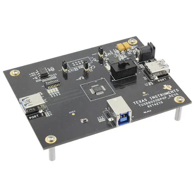
TUSB8020BPHP REVA Evaluation Module
User's Guide
Literature Number: SLLU196
March 2014
�Contents
1
Introduction ......................................................................................................................... 3
2
1
2
Hardware Overview .............................................................................................................. 4
TUSB8020BPHP ................................................................................................................... 4
USB Port Connectors ........................................................................................................... 4
2.1
USB Port Connector - Power ........................................................................................... 4
2.2
USB Port Connector – Noise Filtering ................................................................................. 4
Optional Serial EEPROM .......................................................................................................
Power .................................................................................................................................
Hub Configuration ................................................................................................................
Optional Circuitry .................................................................................................................
5
5
5
5
3
Hardware Set Up ..................................................................................................................
1
Configuration Switches.........................................................................................................
2
EVM Installation ...................................................................................................................
3
Troubleshooting ..................................................................................................................
Appendix A TUSB8020BPHPEVM Bill of Materials ............................................................................
Appendix B Schematics ................................................................................................................
6
6
7
7
8
9
3
4
5
6
2
Table of Contents
SLLU196 – March 2014
Submit Documentation Feedback
Copyright © 2014, Texas Instruments Incorporated
�SLLU196 – March 2014
Introduction
The Texas Instruments TUSB8020BPHP REVA evaluation module is a functional board design of a single
device that implements both a USB 3.0 hub and a USB 2.0 hub. The EVM can support both SuperSpeed
(SS) and USB 2.0 (HS, FS, and LS) operation on its USB ports. This EVM is intended for use in
evaluating system compatibility, developing optional EEPROM firmware, and validating interoperability.
This EVM also acts as a hardware reference design for any implementation of the TUSB8020B.
Upon request, layout files for the EVM can be provided to illustrate techniques used to route the
differential pairs, use of split power planes, placement of filters and other critical components, and
methods used to achieve length matching of critical signals.
NOTE: The EVM accommodates various lab test components, actual production implementations can be much
smaller.
Figure 1. TUSB8020B REVA Top Layer Layout
Microsoft, Windows are registered trademarks of Microsoft Corporation.
SLLU196 – March 2014
Submit Documentation Feedback
Introduction
Copyright © 2014, Texas Instruments Incorporated
3
�SLLU196 – March 2014
Hardware Overview
The TUSB8020B EVM board hardware is divided into the following functional areas:
1
TUSB8020BPHP
The TUSB8020B on the TUSB8020B EVM (U2 on the schematic) operates as a functional interconnect
between an upstream connection to a USB host or hub and up to two directly connected downstream
devices or hubs. More devices and hubs can be supported, if arranged in tiers. The TUSB8020B is
capable of supporting operation at USB SuperSpeed (SS), High-Speed (HS), Full Speed (FS) or Low
Speed (LS). In general, the speed of the upstream connection of the TUSB8020B EVM limits the
downstream connections to that speed (SS, HS, and FS) or lower.
The TUSB8020B requires a 24-MHz low ESR crystal, Y1 with a 1-MΩ feedback resistor. The crystal
should be fundamental mode with a load capacitance of 12 pF – 24 pF and a frequency stability rating of
±100 PPM, or better. To ensure a proper startup oscillation condition, a maximum crystal equivalent series
resistance (ESR) of 50 Ω is recommended.
The TUSB8020B can also use an oscillator or other clock source. When using an external clock source
such as an oscillator, the reference clock should have ±100 PPM (or better) frequency stability and have
less than 50-ps absolute peak- to-peak jitter (or less) than 25-ps peak-to-peak jitter after applying the USB
3.0 jitter transfer function.
2
USB Port Connectors
The TUSB8020B EVM is equipped with three standard nine pin USB 3.0 port connectors. One of these
three connectors, J3, is a Type B connector designed to interface with an upstream USB host or hub. The
remaining connectors, J1 and J4, are Type A connectors for connection to downstream devices or hubs.
Standard size connectors were used on the EVM design, but USB micro connectors can be used if
desired. It is also possible to implement a legacy USB connector on one or more of the downstream ports
if SuperSpeed operation is not desired.
The USB ports can be attached via a standard USB cable to any USB 3.0 or legacy USB host, hub or
device. The TUSB8020B automatically connects to any upstream USB 3.0 host or hub at both
SuperSpeed and High-Speed. Using a legacy USB cable between the TUSB8020B EVM and a USB 3.0
host or hub forces it to High-Speed operation. The same is true if a legacy USB cable is used between the
TUSB8020B EVM and a downstream SuperSpeed capable device: operation is limited to USB 2.0 HighSpeed.
2.1
USB Port Connector - Power
VBUS is received from the upstream host or hub on J3. The TUSB8020B is configured as a self-powered
hub, so there is not any significant current draw by the EVM from VBUS. The TUSB8020B does monitor
the VBUS input after filtering through a resistor divider network of a 90.9-kΩ, 1% resistor, R9, and a 10kΩ, 1% resistor, R10. VBUS cannot be directly connected to the TUSB8020B device. A bulk capacitor of
at least 1 μF is required on the upstream port VBUS input to comply with the USB specification. The
TUSB8020BEVM uses a 10-μF capacitor, C8.
2.2
USB Port Connector – Noise Filtering
Each downstream VBUS output has a 150-μF bulk capacitor (C49, C51) as recommended by the
TPS2561 data manual (SLVS930) to prevent in-rush current events on the downstream devices. In
addition, there are ferrite beads and small capacitors on the VBUS lines to reduce noise and address
ESD/EMI concerns.
4
Hardware Overview
SLLU196 – March 2014
Submit Documentation Feedback
Copyright © 2014, Texas Instruments Incorporated
�Optional Serial EEPROM
www.ti.com
The TUSB8020BEVM also implements optional isolation using two small noise filtering capacitors and a 1MΩ resistor between the earth ground of each connector and the digital ground of the EVM, this is not a
requirement but should be used if ground isolation is desired.
Please note that the series capacitors implemented on the SS TX pairs are incorporated to satisfy the
USB 3.0 requirement that differential links be AC coupled on the transmit pair.
3
Optional Serial EEPROM
Each TUSB8020BEVM is equipped with an onboard EEPROM/socket placeholder, U1. A small I2C
EEPROM can be installed to set the configuration registers as defined in the TUSB8020B data sheet
(SLLSEF6). In its default setting, the EVM does not have an EEPROM installed and instead uses the
configuration inputs to determine any optional settings of the TUSB8020B.
The EEPROM interface defaults to programmable (not write-protected) so that any installed EEPROM’s
contents may be modified to test various settings. If an EEPROM data change is required, the values may
be changed using the register access methods outlined in the TUSB8020B data sheet. In addition, a
Microsoft® Windows® based EEPROM utility is available upon request.
4
Power
The TUSB8020B EVM operates from the power provided by a 5-V wall power adapter, J5, not bus power
supplied by a USB host. TI recommends using a wall power adapter that is capable of sourcing 2 A to 3 A
because the hub must be able to source significant power on its downstream ports (900 mA per port).
The TUSB8020B EVM uses a single-channel LDO voltage regulator to drop 5 V to 3.3 V. The
TPS7A4533, U4, is a 1.5-A output linear regulator (SLVS720). The 1.1-V core voltage required by the
TUSB8020B is sourced by the 3.3-V rail to reduce unnecessary heat dissipation. The TPS74801, U5, is a
1.5-A output single channel LDO linear regulator (SBVS074). Both regulators require few external passive
components and are appropriately rated for heat dissipation.
5
Hub Configuration
The TUSB8020BEVM can be configured by setting several inputs to the TUSB8020B that are sampled at
power-on reset or using an optional serial EEPROM or SMBUS host. A production implementation without
EEPROM or SMBUS could either rely on the default internal pull-up or pull-down resistor for each
configuration input or override it with an external pull-up or pull-down resistor. The settings can be
modified using SW1 on the EVM. Descriptions of the possible configuration changes are included in the
Configuration Switches section.
6
Optional Circuitry
The TUSB8020B EVM design implements a variety of LEDs, none of which are required by the USB
specification. They are provided to make testing and debug easier.
• D1 – Indicates that the upstream USB port is connected at High-Speed.
• D2 - Indicates that the downstream USB port 2 is connected at SuperSpeed.
• D3 – Indicates that the downstream USB port 1 is connected at SuperSpeed.
• D4 – Indicates that the upstream USB port is connected at SuperSpeed.
• D5 – Indicates that 5 V is being applied to the TUSB8020B EVM.
• D6 – Indicates downstream USB port 1 power is on.
• D7 – Indicates downstream USB port 2 power is on.
• D8 – Indicates BOARD_3P3V is active
The switches (SW1 and SW3) and headers (J2, J7, J8, JP1) present on the TUSB8020B EVM are
intended for lab evaluation only and are not required for production designs.
SLLU196 – March 2014
Submit Documentation Feedback
Hardware Overview
Copyright © 2014, Texas Instruments Incorporated
5
�SLLU196 – March 2014
Hardware Set Up
1
Configuration Switches
The TI TUSB8020BEVM has a set of switches to facilitate configuration changes. Changing these switch
settings without a complete understanding of the result is not recommended. Configuration inputs are only
read by the TUSB8020B during power on reset, changing the switch settings while the EVM is powered on
has no effect. Refer to the EVM schematic in Appendix B for additional information .
The switch definitions are as follows, with the standard setting in parenthesis:
SW1_1 (on): FULLPWRMGMTZ_SMBA1_SS Switch. The TUSB8020B has an internal pull up on this
terminal, so the TUSB8020B defaults to a non full power management mode. If the switch is set to the ON
position, the terminal is pulled low and full power management mode is enabled. This means that the
TUSB8020B reports that it supports downstream port power switching in the USB descriptors it sends to
the USB host. Since the TUSB8020B EVM does implement downstream port power switching, enable full
power management mode.
SW1_2 (off): PWRCTL_POL_SS_DN1 Switch. The TUSB8020B has an internal pull down on this
terminal, so port power control polarity defaults to active high. If the switch is set to the ON position, the
terminal is pulled high and the port power control polarity changes to active low.
SW1_3 (off): SMBUSz_SS_DN2 Switch. The TUSB8020B has an internal pull up on this terminal, so I2C
interface mode is enabled by default. If the switch is set to the ON position, the terminal is pulled low and
SMBUS mode is enabled.
SW1_4 (on): GANGED_SMBA2_HS Switch. The TUSB8020B has an internal pull up on this terminal, so
ganged mode is enabled by default. If the switch is set to the ON position, the terminal is pulled low and
individual port power control mode is enabled. Since the TUSB8020B EVM does implement individual port
power controls, this terminal should be set high.
SW1_5 (off): SCL_SMBCLK Switch. The TUSB8020B has an internal pull down on this terminal, so the
serial EEPROM/SMBUS interface is disabled. If the switch is set to the ON position, a pull up resistor is
connected to the serial clock terminal to indicate that an I2C EEPROM may be attached (along with a pull
up resistor on SDA).
SW1_6 (off): SDA_SMBDAT Switch. The TUSB8020B has an internal pull down on this terminal, so the
serial EEPROM/SMBUS interface is disabled. If the switch is set to the ON position, a pull up resistor is
connected to the serial clock terminal to indicate that an I2C EEPROM may be attached (along with a pull
up resistor on SCL).
SW1_7 (off): PWRCTL1_BATEN1 Switch. The TUSB8020B has an internal pull down on this terminal, so
USB Battery Charging mode on Port 1 is disabled by default. If the switch is set to the ON position, the
terminal is pulled high and battery charging is enabled on downstream port 1.
SW1_8 (off): PWRCTL2_BATEN2 Switch. The TUSB8020B has an internal pull down on this terminal, so
USB Battery Charging mode on Port 2 is disabled by default. If the switch is set to the ON position, the
terminal is pulled high and battery charging is enabled on downstream port 2.
6
Hardware Set Up
SLLU196 – March 2014
Submit Documentation Feedback
Copyright © 2014, Texas Instruments Incorporated
�EVM Installation
www.ti.com
2
EVM Installation
Install the EVM using the following steps:
1. Attach a 5-V, 3-A wall power source to J5. LED D5 should turn on.
2. Turn on switch SW3, LED D8 should turn on.
3. Attach a USB cable between J3 and a USB host. LEDs D6 and D7 should turn on.
(a) If the EVM is attached to a USB 3.0 host, D1 and D4 should turn on.
(b) If the EVM is attached to a USB 2.0 host, D1 should turn on.
3
Troubleshooting
Case 1: Device function(s) are “banged out” in Device Manager.
• Make sure that the latest updates are installed for the operating system.
• Make sure that the latest drivers are installed for the host controller.
Case 2: The EVM does not work at all.
• Verify that all switches are in their default state and the EVM is powered on with a 5-V source with
adequate current to support any bus-powered devices (3 A+).
• If installed, remove the serial EEPROM from the EEPROM socket. The EVM does not require an
EEPROM to operate.
• Make sure shunts are installed on J2, J7, and J8.
• In the case where a 12-V power supply has been attached to the EVM, the fault is non-recoverable.
SLLU196 – March 2014
Submit Documentation Feedback
Hardware Set Up
Copyright © 2014, Texas Instruments Incorporated
7
�www.ti.com
Appendix A TUSB8020BPHPEVM Bill of Materials
Table 1 contains the BOM for the EVM.
Table 1. TUSB8020BPHPEVM Bill of Materials
Item
Quantity
Reference
Part
Manufacturer
Part Number
Pkg
1
2
C7,C20
1uF
TDK
C2012X7R1A105K
805
2
3
C4,C12,C16,
0.001uF
TDK
C1005X7R1H102K
402
3
8
C21,C26,C27,C30,C34,C37,C40,C43
0.001uF
TDK
C0603X7R1E102K
201
4
8
C22,C24,C28,C31,C35,C38,C41,C44
0.01uF
TDK
C0603X5R1A103K
201
5
9
C3,C5,C6,C11,C13,C17,C46,C48,C50
0.1uF
Yageo
CC0402KRX5R6BB104
402
6
14
C1,C2,C9,C10,C14,C15,C23,C25,C29,C3
2,C36,C39,C42,C45,
0.1uF
TDK
C0603X5R0J104M
201
7
2
C18,C19
18pF
AVX
04025A180JAT2A
402
8
8
C8,C33,C47,C52,C53,C54,C55, C56
10uF
Murata Electronics
GRM31CR61C106KC31L
1206
9
2
C49,C51
150uF
Kemet
B45197A2157K409 (Tantalum)
7343
10
8
R1,R8,R20,R21,R22,R23,R37
NOPOP
11
8
D1,D2,D3,D4,D5,D6,D7,D8
LED Green 0805
Lite On
LTST-C171GKT
805
12
4
FB1,FB2,FB3,FB4
220 @ 100MHZ Ferrite Bead
Murata
BLM18PG221SN1D
603
13
1
SW1
8-POS 50-MIL SMT
C&K Components
SD08H0SBR
14
1
J3
USB3_TYPEB_CONNECTOR
FoxConn
UEB1112C-2AK1-4H
9_RA_TH_B
15
2
J1,J4
USB3_TYPEA_CONNECTOR
FoxConn
UEA1112C-4HK1-4H
9_RA_TH_A
16
1
J5
2.1mm x 5.5mm DC Power
Jack
CUI Inc.
PJ-202AH (PJ-002AH)
2.1mm x 5.5mm
17
4
R2,R12,R13,R14
1M
Rohm Semiconductor
MCR01MZPJ105
402
18
1
R9
90.9K 1%
Rohm Semiconductor
MCR01MZPF9092
402
19
2
R31,R32
10K
Rohm Semiconductor
MCR01MZPJ103
402
20
1
R10
10K 1%
Rohm Semiconductor
MCR01MZPF1002
402
21
12
R15,R16,R17,R18,R19,R24,R25,R26,
R27,R28,R29, R30
4.7K
Vishay / Dale
CRCW04024K70FKED
402
22
5
R3,R4,R5,R7,R11
1K
Rohm Semiconductor
MCR01MZPJ102
402
23
4
R33,R35,R36,R39
330
Rohm Semiconductor
MCR01MZPJ331
402
24
1
R34
25.5K
Panasonic - ECG
ERJ-2RKF2552X
402
25
1
R38
1.87K
Vishay / Dale
CRCW04021K87FKED
402
26
1
R40
4.99K
Vishay / Dale
CRCW04024K99FKED
402
27
1
U2
TUSB8020B
Texas Instruments
TUSB8020B
48QFP
28
1
U1
AT24C04 Socket
TE Connectivity
AT24C04A-10PU-1.8 / 2-641260-1
8DIP / 8SOIC
SOCKET
29
1
U3
TPS2561DRC - USB Power
Switch
Texas Instruments
TPS2561DRC
10SON
30
1
U4
TPS7A4533 - 3.3V Voltage
Regulator
Texas Instruments
TPS7A4533KTT
DDPAK-5
31
1
U5
TPS74801RGW - 1.1V Voltage
Regulator
Texas Instruments
TPS74801RGW
20VQFN
32
1
Y1
ECS-24MHZ Crystal
ECS
ECX-53B (ECS-240-20-30B-TR)
5.0mm x 3.2mm
33
1
JP1
Conn 2x5 shroud - NOPOP
34
1
R6
9.09K 1%
Panasonic - ECG
ERJ-2RKF9091X
402
35
2
GND1,GND2
TEST POINT - NOPOP
36
1
J2,J7,J8
Header 1x2
3M
961102-6404-AR
37
1
SW3
L101_switch
C&K Components
L101011MS02Q
8
402
TUSB8020BPHPEVM Bill of Materials
SLLU196 – March 2014
Submit Documentation Feedback
Copyright © 2014, Texas Instruments Incorporated
�www.ti.com
Appendix B Schematics
Figure 2 and Figure 3 contain the schematics for this EVM.
FB1
2
DN2_VBUS
DN2_VBUS
VBUS_DS2
220 @ 100MHZ
CAP_DN2_TXP
C1
CAP_DN2_TXM
J1
1
2
3
4
5
6
7
8
9
10
11
USB_DM_DN2
USB_DP_DN2
USB_SSTXP_DN2
0.1uF 0201
C2
C6
0.1uF
USB_SSRXM_DN2
USB_SSRXP_DN2
USB_SSTXM_DN2
0.1uF 0201
CAP_DN2_TXM
CAP_DN2_TXP
USB_SSRXP_DN2
USB_SSRXM_DN2
PWRCTL_POL_SS_DN1_TDO
SMBUSZ_SS_DN2
C4
0.001uF
R2
1M
0402
5%
U1
1
2
3
4
C5
0.1uF
R4
1K
0402
5%
R3
1K
0402
5%
GRSTZ_TCK
VDD33
C3
0.1uF
Optional EEPROM Circuitry
USB3_TY PEA_CONNECTOR
R6
9.09K
0402
1%
VDD33VDD11
BOARD_3P3V
VBUS
DM
DP
GND
SSRXN
SSRXP
GND
SSTXN
SSTXP
SHIELD0
SHIELD1
A0
A1
A2
GND
R5
1K
0402
5%
VCC
WP
SCLK
SDATA
8
7
6
5
R1
NOPOP
SCL_SMBCLK_SSC_DIS
SDA_SMBDAT_U1U2_DIS
AT24C04
R7
1K
0402
5%
C7
1uF
24
23
22
21
20
19
18
17
16
15
14
13
R8
NOPOP
J3
1
2
3
4
5
6
7
8
9
10
11
VBUS
DM
DP
GND
SSTXN
SSTXP
GND
SSRXN
SSRXP
SHIELD0
SHIELD1
25
26
27
28
29
30
31
32
33
34
35
36
USB_DP_UP
USB_DM_UP
VBUS
CAP_UP_TXM
CAP_UP_TXP
C9
0.1uF 0201
C10
0.1uF 0201
USB_SSTXM_UP
USB_SSTXP_UP
USB_SSRXM_UP
USB_SSRXP_UP
GANGED_SMBA2_HS
FULLPWRMGMTZ_SMBA1_SS
C11
0.1uF
C12
0.001uF
VDD33
USB_DP_UP
USB_DM_UP
USB_SSTXM_UP
USB_SSTXP_UP
VDD11
USB_SSRXM_UP
USB_SSRXP_UP
VDD33
VDD11
GANGED / HS_UP
FULLPWRMGMTz / SS_UP
VDD33
XI
XO
VDD33
USB_DP_DN1
USB_DM_DN1
USB_SSTXP_DN1
USB_SSTXM_DN1
VDD11
USB_SSRXP_DN1
USB_SSRXM_DN1
VDD33
USB3_TY PEB_CONNECTOR
R12
1M
0402
5%
J2
VBUS_TMS 2
TEST_TRSTZ
R10
10K 1%
0402
1%
1
VBUS
R11
1K
VDD11
GRSTz_TCK
TEST_TRSTZ
VBUS_DETECT_TMS
OVERCUR2Z
VDD33
PWRCTRL2/BATEN2
OVERCUR1Z_TDI
PWRCTL1/BATEN1
SDA / U1U2_DIS
SCL / SSC_DIS
VDD11
PAD
12
11
10
9
8
7
6
5
4
3
2
1
Header 1x2
90.9K
0402
1%
C8
10uF
VBUS_DETECT_TMS
OVERCUR2Z
2
PWRCTRL2_BATEN2
OVERCUR1Z_TDI
2
PWRCTRL1_BATEN1
OVERCUR1Z_TDI
SDA_SMBDAT_U1U2_DIS
SCL_SMBCLK_SSC_DIS
2
2
49
FB2
2
DN1_VBUS
DN1_VBUS
220 @ 100MHZ
C13
0.1uF
J4
37
38
39
40
41
42
43
44
45
46
47
48
TUSB8020B
R9
Ironwood_48pin_c13119
USB_R1
VDD33
SMBUSz / SS_DN2
PWRCTL_POL / SS_DN1
USB_SSRXM_DN2
USB_SSRXP_DN2
VDD11
USB_SSTXM_DN2
USB_SSTXP_DN2
USB_DM_DN2
USB_DP_DN2
VDD33
U2
R13
USB_SSRXM_DN1
USB_SSRXP_DN1
USB_SSTXM_DN1
USB_SSTXP_DN1
USB_DM_DN1
USB_DP_DN1
1M
1
2
3
4
5
6
7
8
9
10
11
VBUS_DS1
USB_SSRXM_DN1
USB_SSRXP_DN1
USB_SSTXM_DN1
0.1uF 0201
C14
USB_SSTXP_DN1
0.1uF 0201
C15
CAP_DN_TXM1
CAP_DN_TXP1
VBUS
DM
DP
GND
SSRXN
SSRXP
GND
SSTXN
SSTXP
SHIELD0
SHIELD1
USB3_TY PEA_CONNECTOR
R14
1M
0402
5%
Y1
BOARD_3P3V
C16
0.001uF
C17
0.1uF
ECS-24MHZ
0402
5%
R17
0402
5%
R18
0402
5%
C18
C19
18pF
18pF
BOARD_3P3V
R19
0402
5%
FULLPWRZ
PWRCTL_POL
SMBUSZ
GANGED
SSC_DIS
U1U2_DIS
BATEN1
BATEN2
R24
R25
R26
0402
5%
0402
5%
0402
5%
SW1
8-POS 50-MIL SMT
C&K (ITT-CANNON)
TDA08H0SK1R
16
1
15
2
14
3
13
4
12
5
11
6
10
7
9
8
FULLPWRMGMTZ_SMBA1_SS
PWRCTL_POL_SS_DN1_TDO
SMBUSZ_SS_DN2
GANGED_SMBA2_HS
SCL_SMBCLK_SSC_DIS
SDA_SMBDAT_U1U2_DIS
PWRCTRL1_BATEN1
PWRCTRL2_BATEN2
R20
NOPOP
R21
NOPOP
R22
NOPOP
R23
NOPOP
1
3
5
7
9
TEST_TRSTZ
PWRCTL_POL_SS_DN1_TDO
OVERCUR1Z_TDI
VBUS_TMS
GRSTZ_TCK
JP1
2
4
6
8
10
Conn 2x5 shroud
JTAG is for lab evaluation only.
This header and NOPOP pullups are not recommended
for customers.
D1
LED
D2
LED
US HS
D3
LED
SS DN2
D4
LED
SS DN1
R27
R28
R29
R30
0402
5%
0402
5%
0402
5%
0402
5%
SS US
VDD33
BOARD_3P3V
FB3
1
C21
C20
1uF
0.001uF
C22
0.01uF
C23
C24
C25
0.1uF
0.01uF
0.1uF
C26
0.001uF
C27
C28
C29
C30
C31
C32
0.001uF
0.01uF
0.1uF
0.001uF
0.01uF
0.1uF
J7
2
220 @ 100MHZ
Header 1x2
Label as 3.3V in silkscreen
BOARD_1P1V
VDD11
FB4
1
C33
10uF
C34
C35
C36
C37
C38
C39
C40
C41
C42
C43
C44
C45
0.001uF
0.01uF
0.1uF
0.001uF
0.01uF
0.1uF
0.001uF
0.01uF
0.1uF
0.001uF
0.01uF
0.1uF
J8
2
GND2
GND1
220 @ 100MHZ
Header 1x2
1
0402
5%
R16
1
R15
Label as 1.1V in silkscreen
Figure 2. TUSB8020BPHPEVM Schematic
SLLU196 – March 2014
Submit Documentation Feedback
Schematics
Copyright © 2014, Texas Instruments Incorporated
9
�Appendix B
www.ti.com
5V INPUT
BOARD_3P3V
DOWNSTREAM PORT POWER SWITCH
BOARD_5V
SILKSCREEN: TIP +5v
BOARD_3P3V
BOARD_5V
J5
2
3
1
R31
10K
0402
5%
SW3
C46
S
T
L101011MS02Q
2.1mm x 5.5mm
C56
10uF
0.1uF
LED5V
C47
10uF
U3
2
3
R33
330
0402
5%
1
PWRCTRL1_BATEN1
1
PWRCTRL2_BATEN2
PWRCTRL1_BATEN1
4
PWRCTRL2_BATEN2
5
1
11
D5
LED Green 0805
R32
10K
0402
5%
IN
IN
OUT1
FAULT1Z
EN1
OUT2
EN2
FAULT2Z
GND
PAD
ILIM
9
DN1_VBUS
DN1_VBUS
10
1
OVERCUR1Z_TDI
8
DN2_VBUS
DN2_VBUS
6
OVERCUR2Z
7
ILIM1
1
C50
C48
0.1uF
TPS2561
1
1
+
R34
25.5K
0402
5%
C49
150uF
0.1uF
+
C51
150uF
D6
LED Green 0805
D7
LED Green 0805
Limiting DS Port VBUS current to 2.2A per port.
R35
330
0402
5%
R36
330
0402
5%
1.1V REGULATOR
BOARD_5V
3.3V REGULATOR
1P1V_SS
BOARD_3P3V
BOARD_3P3V
D8
LED Green 0805
C54
10uF
10
R39
330
0402
5%
2
3
4
13
14
17
15
NC1
NC2
NC3
NC4
NC5
NC6
SS
IN1
IN2
IN3
IN4
EN
BIAS
TPS74801RGW
OUT1
OUT2
OUT3
OUT4
FB
PAD
C52
10uF
GND
5
5
6
7
8
11
21
TAB
SENSE
U5
4
12
TPS7A4533
GND
SHDN/
OUT
6
1
C53
10uF
IN
3
2
BOARD_1P1V
R37
NOPOP
U4
PG
1
18
19
20
16
9
1P1V_FB
R38
1.87K
0402
5%
C55
10uF
R40
4.99K
0402
5%
Figure 3. TUSB8020BPHPEVM Power Schematic
10
Schematics
SLLU196 – March 2014
Submit Documentation Feedback
Copyright © 2014, Texas Instruments Incorporated
�ADDITIONAL TERMS AND CONDITIONS, WARNINGS, RESTRICTIONS, AND DISCLAIMERS FOR
EVALUATION MODULES
Texas Instruments Incorporated (TI) markets, sells, and loans all evaluation boards, kits, and/or modules (EVMs) pursuant to, and user
expressly acknowledges, represents, and agrees, and takes sole responsibility and risk with respect to, the following:
1.
User agrees and acknowledges that EVMs are intended to be handled and used for feasibility evaluation only in laboratory and/or
development environments. Notwithstanding the foregoing, in certain instances, TI makes certain EVMs available to users that do not
handle and use EVMs solely for feasibility evaluation only in laboratory and/or development environments, but may use EVMs in a
hobbyist environment. All EVMs made available to hobbyist users are FCC certified, as applicable. Hobbyist users acknowledge, agree,
and shall comply with all applicable terms, conditions, warnings, and restrictions in this document and are subject to the disclaimer and
indemnity provisions included in this document.
2. Unless otherwise indicated, EVMs are not finished products and not intended for consumer use. EVMs are intended solely for use by
technically qualified electronics experts who are familiar with the dangers and application risks associated with handling electrical
mechanical components, systems, and subsystems.
3. User agrees that EVMs shall not be used as, or incorporated into, all or any part of a finished product.
4. User agrees and acknowledges that certain EVMs may not be designed or manufactured by TI.
5. User must read the user's guide and all other documentation accompanying EVMs, including without limitation any warning or
restriction notices, prior to handling and/or using EVMs. Such notices contain important safety information related to, for example,
temperatures and voltages. For additional information on TI's environmental and/or safety programs, please visit www.ti.com/esh or
contact TI.
6. User assumes all responsibility, obligation, and any corresponding liability for proper and safe handling and use of EVMs.
7. Should any EVM not meet the specifications indicated in the user’s guide or other documentation accompanying such EVM, the EVM
may be returned to TI within 30 days from the date of delivery for a full refund. THE FOREGOING LIMITED WARRANTY IS THE
EXCLUSIVE WARRANTY MADE BY TI TO USER AND IS IN LIEU OF ALL OTHER WARRANTIES, EXPRESSED, IMPLIED, OR
STATUTORY, INCLUDING ANY WARRANTY OF MERCHANTABILITY OR FITNESS FOR ANY PARTICULAR PURPOSE. TI SHALL
NOT BE LIABLE TO USER FOR ANY INDIRECT, SPECIAL, INCIDENTAL, OR CONSEQUENTIAL DAMAGES RELATED TO THE
HANDLING OR USE OF ANY EVM.
8. No license is granted under any patent right or other intellectual property right of TI covering or relating to any machine, process, or
combination in which EVMs might be or are used. TI currently deals with a variety of customers, and therefore TI’s arrangement with
the user is not exclusive. TI assumes no liability for applications assistance, customer product design, software performance, or
infringement of patents or services with respect to the handling or use of EVMs.
9. User assumes sole responsibility to determine whether EVMs may be subject to any applicable federal, state, or local laws and
regulatory requirements (including but not limited to U.S. Food and Drug Administration regulations, if applicable) related to its handling
and use of EVMs and, if applicable, compliance in all respects with such laws and regulations.
10. User has sole responsibility to ensure the safety of any activities to be conducted by it and its employees, affiliates, contractors or
designees, with respect to handling and using EVMs. Further, user is responsible to ensure that any interfaces (electronic and/or
mechanical) between EVMs and any human body are designed with suitable isolation and means to safely limit accessible leakage
currents to minimize the risk of electrical shock hazard.
11. User shall employ reasonable safeguards to ensure that user’s use of EVMs will not result in any property damage, injury or death,
even if EVMs should fail to perform as described or expected.
12. User shall be solely responsible for proper disposal and recycling of EVMs consistent with all applicable federal, state, and local
requirements.
Certain Instructions. User shall operate EVMs within TI’s recommended specifications and environmental considerations per the user’s
guide, accompanying documentation, and any other applicable requirements. Exceeding the specified ratings (including but not limited to
input and output voltage, current, power, and environmental ranges) for EVMs may cause property damage, personal injury or death. If
there are questions concerning these ratings, user should contact a TI field representative prior to connecting interface electronics including
input power and intended loads. Any loads applied outside of the specified output range may result in unintended and/or inaccurate
operation and/or possible permanent damage to the EVM and/or interface electronics. Please consult the applicable EVM user's guide prior
to connecting any load to the EVM output. If there is uncertainty as to the load specification, please contact a TI field representative. During
normal operation, some circuit components may have case temperatures greater than 60°C as long as the input and output are maintained
at a normal ambient operating temperature. These components include but are not limited to linear regulators, switching transistors, pass
transistors, and current sense resistors which can be identified using EVMs’ schematics located in the applicable EVM user's guide. When
placing measurement probes near EVMs during normal operation, please be aware that EVMs may become very warm. As with all
electronic evaluation tools, only qualified personnel knowledgeable in electronic measurement and diagnostics normally found in
development environments should use EVMs.
Agreement to Defend, Indemnify and Hold Harmless. User agrees to defend, indemnify, and hold TI, its directors, officers, employees,
agents, representatives, affiliates, licensors and their representatives harmless from and against any and all claims, damages, losses,
expenses, costs and liabilities (collectively, "Claims") arising out of, or in connection with, any handling and/or use of EVMs. User’s
indemnity shall apply whether Claims arise under law of tort or contract or any other legal theory, and even if EVMs fail to perform as
described or expected.
Safety-Critical or Life-Critical Applications. If user intends to use EVMs in evaluations of safety critical applications (such as life support),
and a failure of a TI product considered for purchase by user for use in user’s product would reasonably be expected to cause severe
personal injury or death such as devices which are classified as FDA Class III or similar classification, then user must specifically notify TI
of such intent and enter into a separate Assurance and Indemnity Agreement.
�RADIO FREQUENCY REGULATORY COMPLIANCE INFORMATION FOR EVALUATION MODULES
Texas Instruments Incorporated (TI) evaluation boards, kits, and/or modules (EVMs) and/or accompanying hardware that is marketed, sold,
or loaned to users may or may not be subject to radio frequency regulations in specific countries.
General Statement for EVMs Not Including a Radio
For EVMs not including a radio and not subject to the U.S. Federal Communications Commission (FCC) or Industry Canada (IC)
regulations, TI intends EVMs to be used only for engineering development, demonstration, or evaluation purposes. EVMs are not finished
products typically fit for general consumer use. EVMs may nonetheless generate, use, or radiate radio frequency energy, but have not been
tested for compliance with the limits of computing devices pursuant to part 15 of FCC or the ICES-003 rules. Operation of such EVMs may
cause interference with radio communications, in which case the user at his own expense will be required to take whatever measures may
be required to correct this interference.
General Statement for EVMs including a radio
User Power/Frequency Use Obligations: For EVMs including a radio, the radio included in such EVMs is intended for development and/or
professional use only in legally allocated frequency and power limits. Any use of radio frequencies and/or power availability in such EVMs
and their development application(s) must comply with local laws governing radio spectrum allocation and power limits for such EVMs. It is
the user’s sole responsibility to only operate this radio in legally acceptable frequency space and within legally mandated power limitations.
Any exceptions to this are strictly prohibited and unauthorized by TI unless user has obtained appropriate experimental and/or development
licenses from local regulatory authorities, which is the sole responsibility of the user, including its acceptable authorization.
U.S. Federal Communications Commission Compliance
For EVMs Annotated as FCC – FEDERAL COMMUNICATIONS COMMISSION Part 15 Compliant
Caution
This device complies with part 15 of the FCC Rules. Operation is subject to the following two conditions: (1) This device may not cause
harmful interference, and (2) this device must accept any interference received, including interference that may cause undesired operation.
Changes or modifications could void the user's authority to operate the equipment.
FCC Interference Statement for Class A EVM devices
This equipment has been tested and found to comply with the limits for a Class A digital device, pursuant to part 15 of the FCC Rules.
These limits are designed to provide reasonable protection against harmful interference when the equipment is operated in a commercial
environment. This equipment generates, uses, and can radiate radio frequency energy and, if not installed and used in accordance with the
instruction manual, may cause harmful interference to radio communications. Operation of this equipment in a residential area is likely to
cause harmful interference in which case the user will be required to correct the interference at its own expense.
FCC Interference Statement for Class B EVM devices
This equipment has been tested and found to comply with the limits for a Class B digital device, pursuant to part 15 of the FCC Rules.
These limits are designed to provide reasonable protection against harmful interference in a residential installation. This equipment
generates, uses and can radiate radio frequency energy and, if not installed and used in accordance with the instructions, may cause
harmful interference to radio communications. However, there is no guarantee that interference will not occur in a particular installation. If
this equipment does cause harmful interference to radio or television reception, which can be determined by turning the equipment off and
on, the user is encouraged to try to correct the interference by one or more of the following measures:
• Reorient or relocate the receiving antenna.
• Increase the separation between the equipment and receiver.
• Connect the equipment into an outlet on a circuit different from that to which the receiver is connected.
• Consult the dealer or an experienced radio/TV technician for help.
Industry Canada Compliance (English)
For EVMs Annotated as IC – INDUSTRY CANADA Compliant:
This Class A or B digital apparatus complies with Canadian ICES-003.
Changes or modifications not expressly approved by the party responsible for compliance could void the user’s authority to operate the
equipment.
Concerning EVMs Including Radio Transmitters
This device complies with Industry Canada licence-exempt RSS standard(s). Operation is subject to the following two conditions: (1) this
device may not cause interference, and (2) this device must accept any interference, including interference that may cause undesired
operation of the device.
Concerning EVMs Including Detachable Antennas
Under Industry Canada regulations, this radio transmitter may only operate using an antenna of a type and maximum (or lesser) gain
approved for the transmitter by Industry Canada. To reduce potential radio interference to other users, the antenna type and its gain should
be so chosen that the equivalent isotropically radiated power (e.i.r.p.) is not more than that necessary for successful communication.
This radio transmitter has been approved by Industry Canada to operate with the antenna types listed in the user guide with the maximum
permissible gain and required antenna impedance for each antenna type indicated. Antenna types not included in this list, having a gain
greater than the maximum gain indicated for that type, are strictly prohibited for use with this device.
�Canada Industry Canada Compliance (French)
Cet appareil numérique de la classe A ou B est conforme à la norme NMB-003 du Canada
Les changements ou les modifications pas expressément approuvés par la partie responsable de la conformité ont pu vider l’autorité de
l'utilisateur pour actionner l'équipement.
Concernant les EVMs avec appareils radio
Le présent appareil est conforme aux CNR d'Industrie Canada applicables aux appareils radio exempts de licence. L'exploitation est
autorisée aux deux conditions suivantes : (1) l'appareil ne doit pas produire de brouillage, et (2) l'utilisateur de l'appareil doit accepter tout
brouillage radioélectrique subi, même si le brouillage est susceptible d'en compromettre le fonctionnement.
Concernant les EVMs avec antennes détachables
Conformément à la réglementation d'Industrie Canada, le présent émetteur radio peut fonctionner avec une antenne d'un type et d'un gain
maximal (ou inférieur) approuvé pour l'émetteur par Industrie Canada. Dans le but de réduire les risques de brouillage radioélectrique à
l'intention des autres utilisateurs, il faut choisir le type d'antenne et son gain de sorte que la puissance isotrope rayonnée équivalente
(p.i.r.e.) ne dépasse pas l'intensité nécessaire à l'établissement d'une communication satisfaisante.
Le présent émetteur radio a été approuvé par Industrie Canada pour fonctionner avec les types d'antenne énumérés dans le manuel
d’usage et ayant un gain admissible maximal et l'impédance requise pour chaque type d'antenne. Les types d'antenne non inclus dans
cette liste, ou dont le gain est supérieur au gain maximal indiqué, sont strictement interdits pour l'exploitation de l'émetteur.
Mailing Address: Texas Instruments, Post Office Box 655303, Dallas, Texas 75265
Copyright © 2014, Texas Instruments Incorporated
spacer
Important Notice for Users of EVMs Considered “Radio Frequency Products” in Japan
EVMs entering Japan are NOT certified by TI as conforming to Technical Regulations of Radio Law of Japan.
If user uses EVMs in Japan, user is required by Radio Law of Japan to follow the instructions below with respect to EVMs:
1.
2.
3.
Use EVMs in a shielded room or any other test facility as defined in the notification #173 issued by Ministry of Internal Affairs and
Communications on March 28, 2006, based on Sub-section 1.1 of Article 6 of the Ministry’s Rule for Enforcement of Radio Law of
Japan,
Use EVMs only after user obtains the license of Test Radio Station as provided in Radio Law of Japan with respect to EVMs, or
Use of EVMs only after user obtains the Technical Regulations Conformity Certification as provided in Radio Law of Japan with respect
to EVMs. Also, do not transfer EVMs, unless user gives the same notice above to the transferee. Please note that if user does not
follow the instructions above, user will be subject to penalties of Radio Law of Japan.
http://www.tij.co.jp
【無線電波を送信する製品の開発キットをお使いになる際の注意事項】 本開発キットは技術基準適合証明を受けておりません。 本製品の
ご使用に際しては、電波法遵守のため、以下のいずれかの措置を取っていただく必要がありますのでご注意ください。
1.
2.
3.
電波法施行規則第6条第1項第1号に基づく平成18年3月28日総務省告示第173号で定められた電波暗室等の試験設備でご使用いただく。
実験局の免許を取得後ご使用いただく。
技術基準適合証明を取得後ご使用いただく。。
なお、本製品は、上記の「ご使用にあたっての注意」を譲渡先、移転先に通知しない限り、譲渡、移転できないものとします
上記を遵守頂けない場合は、電波法の罰則が適用される可能性があることをご留意ください。
日本テキサス・インスツルメンツ株式会社
東京都新宿区西新宿6丁目24番1号
西新宿三井ビル
http://www.tij.co.jp
Texas Instruments Japan Limited
(address) 24-1, Nishi-Shinjuku 6 chome, Shinjuku-ku, Tokyo, Japan
�IMPORTANT NOTICE
Texas Instruments Incorporated and its subsidiaries (TI) reserve the right to make corrections, enhancements, improvements and other
changes to its semiconductor products and services per JESD46, latest issue, and to discontinue any product or service per JESD48, latest
issue. Buyers should obtain the latest relevant information before placing orders and should verify that such information is current and
complete. All semiconductor products (also referred to herein as “components”) are sold subject to TI’s terms and conditions of sale
supplied at the time of order acknowledgment.
TI warrants performance of its components to the specifications applicable at the time of sale, in accordance with the warranty in TI’s terms
and conditions of sale of semiconductor products. Testing and other quality control techniques are used to the extent TI deems necessary
to support this warranty. Except where mandated by applicable law, testing of all parameters of each component is not necessarily
performed.
TI assumes no liability for applications assistance or the design of Buyers’ products. Buyers are responsible for their products and
applications using TI components. To minimize the risks associated with Buyers’ products and applications, Buyers should provide
adequate design and operating safeguards.
TI does not warrant or represent that any license, either express or implied, is granted under any patent right, copyright, mask work right, or
other intellectual property right relating to any combination, machine, or process in which TI components or services are used. Information
published by TI regarding third-party products or services does not constitute a license to use such products or services or a warranty or
endorsement thereof. Use of such information may require a license from a third party under the patents or other intellectual property of the
third party, or a license from TI under the patents or other intellectual property of TI.
Reproduction of significant portions of TI information in TI data books or data sheets is permissible only if reproduction is without alteration
and is accompanied by all associated warranties, conditions, limitations, and notices. TI is not responsible or liable for such altered
documentation. Information of third parties may be subject to additional restrictions.
Resale of TI components or services with statements different from or beyond the parameters stated by TI for that component or service
voids all express and any implied warranties for the associated TI component or service and is an unfair and deceptive business practice.
TI is not responsible or liable for any such statements.
Buyer acknowledges and agrees that it is solely responsible for compliance with all legal, regulatory and safety-related requirements
concerning its products, and any use of TI components in its applications, notwithstanding any applications-related information or support
that may be provided by TI. Buyer represents and agrees that it has all the necessary expertise to create and implement safeguards which
anticipate dangerous consequences of failures, monitor failures and their consequences, lessen the likelihood of failures that might cause
harm and take appropriate remedial actions. Buyer will fully indemnify TI and its representatives against any damages arising out of the use
of any TI components in safety-critical applications.
In some cases, TI components may be promoted specifically to facilitate safety-related applications. With such components, TI’s goal is to
help enable customers to design and create their own end-product solutions that meet applicable functional safety standards and
requirements. Nonetheless, such components are subject to these terms.
No TI components are authorized for use in FDA Class III (or similar life-critical medical equipment) unless authorized officers of the parties
have executed a special agreement specifically governing such use.
Only those TI components which TI has specifically designated as military grade or “enhanced plastic” are designed and intended for use in
military/aerospace applications or environments. Buyer acknowledges and agrees that any military or aerospace use of TI components
which have not been so designated is solely at the Buyer's risk, and that Buyer is solely responsible for compliance with all legal and
regulatory requirements in connection with such use.
TI has specifically designated certain components as meeting ISO/TS16949 requirements, mainly for automotive use. In any case of use of
non-designated products, TI will not be responsible for any failure to meet ISO/TS16949.
Products
Applications
Audio
www.ti.com/audio
Automotive and Transportation
www.ti.com/automotive
Amplifiers
amplifier.ti.com
Communications and Telecom
www.ti.com/communications
Data Converters
dataconverter.ti.com
Computers and Peripherals
www.ti.com/computers
DLP® Products
www.dlp.com
Consumer Electronics
www.ti.com/consumer-apps
DSP
dsp.ti.com
Energy and Lighting
www.ti.com/energy
Clocks and Timers
www.ti.com/clocks
Industrial
www.ti.com/industrial
Interface
interface.ti.com
Medical
www.ti.com/medical
Logic
logic.ti.com
Security
www.ti.com/security
Power Mgmt
power.ti.com
Space, Avionics and Defense
www.ti.com/space-avionics-defense
Microcontrollers
microcontroller.ti.com
Video and Imaging
www.ti.com/video
RFID
www.ti-rfid.com
OMAP Applications Processors
www.ti.com/omap
TI E2E Community
e2e.ti.com
Wireless Connectivity
www.ti.com/wirelessconnectivity
Mailing Address: Texas Instruments, Post Office Box 655303, Dallas, Texas 75265
Copyright © 2014, Texas Instruments Incorporated
�