User's Guide
SLAU605 – December 2014
TVB1440 EVM
This document describes how to use and configure the TVB1440 EVM, along with recommendations for
system hardware implementation. These recommendations are only guidelines and it is designer’s
responsibility to consider all system characteristics and requirements. The engineers should refer to the
datasheet (SLASE51) for technical details such as device operation, terminal description, and so forth.
1
2
3
4
5
6
7
Contents
Overview ...................................................................................................................... 2
1.1
What is the TVB1440? ............................................................................................. 2
1.2
What is the TVB1440 EVM? ...................................................................................... 2
1.3
What is Included in the TVB1440 EVM?......................................................................... 2
1.4
What Does This EVM Look Like? ................................................................................ 2
Hardware Description ....................................................................................................... 3
2.1
Video Connectors ................................................................................................... 3
2.2
Local I2C Access .................................................................................................... 5
2.3
Enable/Reset ........................................................................................................ 5
2.4
Power ................................................................................................................. 6
2.5
SW2 DIP Switch Configuration.................................................................................... 7
Quick Start Guide ............................................................................................................ 7
References ................................................................................................................... 7
EVM Bill of Materials (BOM) ............................................................................................... 8
EVM Schematics ............................................................................................................. 9
EVM Layout ................................................................................................................. 15
List of Figures
...............................................................................................................
1
TVB1440 EVM
2
TVB1440 EVM Block Diagram ............................................................................................. 3
3
TVB1440 EVM Mechanical Drawing ...................................................................................... 4
4
TVB1440 EVM Schematic (1 of 6)
5
6
7
8
9
10
11
12
13
14
15
2
........................................................................................ 9
TVB1440 EVM Schematic (2 of 6) ....................................................................................... 10
TVB1440 EVM Schematic (3 of 6) ....................................................................................... 11
TVB1440 EVM Schematic (4 of 6) ....................................................................................... 12
TVB1440 EVM Schematic (5 of 6) ....................................................................................... 13
TVB1440 EVM Schematic (6 of 6) ....................................................................................... 14
Layer 1 (Top) ............................................................................................................... 15
Layer 2 (GND) .............................................................................................................. 15
Layer 3 (Power) ............................................................................................................ 16
Layer 4 (Power) ............................................................................................................ 16
Layer 5 (GND) .............................................................................................................. 17
Layer 6 (Bottom)............................................................................................................ 17
List of Tables
1
Video Input Connector (J1) ................................................................................................. 3
2
Video Output Connector (J2) ............................................................................................... 4
3
JMP1 Pin-out ................................................................................................................. 5
SLAU605 – December 2014
Submit Documentation Feedback
TVB1440 EVM
Copyright © 2014, Texas Instruments Incorporated
1
�Overview
www.ti.com
4
SW2 DIP Switch Setting .................................................................................................... 7
5
EVM Bill of Materials ........................................................................................................ 8
1
Overview
1.1
What is the TVB1440?
The TVB1440 is a four-channel re-driver signal conditioner for TV applications, allowing signal integrity
between TV chipset and a TCON. It has selectable control for receive equalization to compensate for
large trace or cable loss at its input resulting in a improved eye at the TVB1440’s output. Each of the
TVB1440 transmitters has independent control for voltage swing and pre-emphasis.
1.2
What is the TVB1440 EVM?
The TVB1440 EVM is a PCB created to help customers evaluate the TVB1440 device for TV applications.
This EVM can also be used as a hardware reference design for implementation of the TVB1440 in the 48pin VQFN (RGZ) package.
PCB design/layout files can be provided upon request to aid PCB design with a TVB1440 component. The
layout files can be used as a guideline to implement the TVB1440 with illustrations of the
routing/placement rules. Please note that the EVM design includes test components to evaluate the
TVB1440 which may not be needed for all applications.
1.3
What is Included in the TVB1440 EVM?
The EVM contains the following major components:
• TVB1440
• SAMTEC connectors for user-defined daughterboards.
• On-board USB to I2C interface for communication with external PC
• I2C programming interface for external I2C host connection
1.4
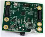
What Does This EVM Look Like?
Figure 1. TVB1440 EVM
2
TVB1440 EVM
SLAU605 – December 2014
Submit Documentation Feedback
Copyright © 2014, Texas Instruments Incorporated
�Hardware Description
www.ti.com
2
Hardware Description
TUSB3410
SCL
OUT0P/N
IN1P/N
SAMTEC
SAMTEC
IN0P/N
SDA
OUT1P/N
TVB1440
(48-pin QFN)
IN2P/N
IN3P/N
OUT2P/N
OUT3P/N
Figure 2. TVB1440 EVM Block Diagram
2.1
Video Connectors
Video into and out of the TVB1440 is supported using the two Samtec QSH (Samtec P/N: QSH-020-01-LD-DP-A) connectors. The input video connector is J1 and the output video connector is J2. Note that the
J2 is rotated on the PCB 180 degrees from J1.
The mating connector part number is QTH-020-01-L-D-DP-A. For SMA-type connection, HDR-128291-XX
breakout board from Samtec can be used. The HDR-128291-XX is a breakout board with a mating
connector to J1 or J2 and standard SMA male connectors via cables.
Table 1. Video Input Connector (J1)
Pin No.
Name
Pin No.
Name
1
IN3N
2
J1J2_SDA_CTL
3
IN3P
4
J1J2_SCL_CTL
5
GND
6
Connected to J2 pin 6
7
GND
8
Connected to J2 pin 8
9
IN2N
10
Connected to J2 pin 10
11
IN2P
12
Connected to J2 pin 12
13
GND
14
Connected to J2 pin 14
15
GND
16
Connected to J2 pin 16
17
IN1N
18
Connected to J2 pin 18
19
IN1P
20
Connected to J2 pin 20
21
GND
22
Connected to J2 pin 22
23
GND
24
Connected to J2 pin 24
25
IN0N
26
J1J2_12V
27
IN0P
28
J1J2_12V
29
GND
30
J1J2_12V
31
GND
32
J1J2_12V
33
NC
34
J1J2_3.3V
35
NC
36
J1J2_3.3V
37
NC
38
J1J2_1.1V
39
NC
40
J1J2_1.1V
SLAU605 – December 2014
Submit Documentation Feedback
TVB1440 EVM
Copyright © 2014, Texas Instruments Incorporated
3
�Hardware Description
www.ti.com
Table 2. Video Output Connector (J2)
Pin No.
Name
Pin No.
Name
1
OUT0P
2
J1J2_SDA_CTL
3
OUT0N
4
J1J2_SCL_CTL
5
GND
6
Connected to J1 pin 6
7
GND
8
Connected to J1 pin 8
9
OUT1P
10
Connected to J1 pin 10
11
OUT1N
12
Connected to J1 pin 12
13
GND
14
Connected to J1 pin 14
15
GND
16
Connected to J1 pin 16
17
OUT2P
18
Connected to J1 pin 18
19
OUT2N
20
Connected to J1 pin 20
21
GND
22
Connected to J1 pin 22
23
GND
24
Connected to J1 pin 24
25
OUT3P
26
J1J2_12V
27
OUT3N
28
J1J2_12V
29
GND
30
J1J2_12V
31
GND
32
J1J2_12V
33
NC
34
J1J2_3.3V
35
NC
36
J1J2_3.3V
37
NC
38
J1J2_1.1V
39
NC
40
J1J2_1.1V
For designers needing to design their own customer daughterboard that mates to the TVB1440 EVM, the
necessary information needed to develop the daughterboard is provided below.
6.350
57.150
ON
SW1
SW2
JMP1
1 2 3 4 5 6 7 8
OUTPUT
U1
5.810
1
2
57.150
2
INPUT
J2
1
J1
31.750
J4
DC JACK
14.190
6.350
6.350
9.180
6.350
6.350
69.850
All Dimensions in mm
ALLDIMENSIONS INMM.
NOTE: All six large plated mounting holes are 160 mils (±3 mils) diameter.
Figure 3. TVB1440 EVM Mechanical Drawing
4
TVB1440 EVM
SLAU605 – December 2014
Submit Documentation Feedback
Copyright © 2014, Texas Instruments Incorporated
�Hardware Description
www.ti.com
2.2
2
Local I C Access
There are three options to access the TVB1440’s local I2C registers:
1. 3-pin 100-mil male header
2. Through USB Micro-AB connect via the TUSB3410
3. Through the SAMTEC connectors J1 and J2
2.2.1
Via 3-Pin 100-mil Male Header
A stand alone external I2C host can be connected via JMP1 for debug and control purposes. An example
of an external I2C Host controller is the Total Phase Aardvark I2C/SPI Host Adapter (Total Phase Part#:
TP240141).
Table 3. JMP1 Pin-out
JMP1
Description
1
SCL_CTL
2
SDA_CTL
3
GND
When using JMP1, it is recommended to make sure SW2-3, SW2-4, SW2-5, and SW2-6 are all in the
“OFF” position.
2.2.2
Via USB Interface
Communication with TVB1440 can also be accomplished using the USB Micro-AB connector (J3) through
the TUSB3410. When using this interface, make sure SW2-5 and SW2-6 are in the “OFF” position, and
SW2-3 and SW-4 are in the “ON” position. Also, if the DC jack is plugged into J4, then make sure the
voltage of the DC jack is greater than 5.5 V.
2.2.3
Via J1/J2 Samtec Connector
Communication with the TVB1440 can also be accomplished through the Samtec connectors J1. If it is
required for the I2C interface to be routed to the second Samtec connector (J2), then resistors R3 and R4
must be populated.
Communication through the Samtec connectors requires that both SW2-5 and SW2-6 are in the “ON”
position, and SW2-3 and SW2-4 are in the “OFF” position.
2.3
Enable/Reset
There are three device enable/reset options to use with the EVM.
1. RC timing option
C28 external capacitor and TVB1440’s internal resistor are used to control the RSTN ramp time after
the device is powered on.
2. External control option
A push button (SW1) available for the manual control of the TVB1440’s RSTN input.
SLAU605 – December 2014
Submit Documentation Feedback
TVB1440 EVM
Copyright © 2014, Texas Instruments Incorporated
5
�Hardware Description
2.4
www.ti.com
Power
EVM provides three means to provide power to the TVB1440:
1. DC Power Jack (J4)
2. USB Micro-AB connector (J3)
3. Samtec connector J1 and J2. By default, either power can be applied via the DC jack or the USB
Micro-AB connector. If power is required through the J1 and J2 connectors, then R1 (for 1.1-V power)
and R2 (for 3.3-V power) must be installed.
Choose only one power source (DC jack, USB Micro-AB, or Samtec J1/J2). If both DC jack and USB
interface are used together, make sure the DC jack power is greater than 5.5 V.
2.4.1
DC Jack (J4)
A DC power jack (J9) to accept a 5-V to 17-V wall power adapter is provided on the EVM. The DC power
jack (CUI Inc. PJ-202AH) has an inner diameter of 2.1 mm and an outer diameter of 5.5 mm. The tip of
the power supply must be positive. A power supply of at least 0.5 A that meets these requirements can be
used to power the TVB1440 EVM.
CAUTION
Care should be taken not to plug in any power source higher than the
configured voltage (5 V to 17 V).
2.4.2
USB Micro-AB
A standard USB Micro-AB connector is included on the EVM to allow for powering the EVM from an
external USB power source.
6
TVB1440 EVM
SLAU605 – December 2014
Submit Documentation Feedback
Copyright © 2014, Texas Instruments Incorporated
�Hardware Description
www.ti.com
2.5
SW2 DIP Switch Configuration
Table 4. SW2 DIP Switch Setting
Default Config
DIP SW No.
SW2.1
SW2.2
TVB1440 I2C Slave Address
SW2-1 (1)
SW2-2 (1)
Address(W/R)
OFF
ON
0x58/59 (Default)
ON
ON
0x5A/5B
ON
OFF
0x5C/5D
ON (Closed)
X
X
SW2-3
X
SW2-4
TUSB3410 connected to TVB1440’s SDA_CTL pin
ON: Connected to SDA_CTL
OFF: Disconnected from SDA_CTL
X
SW2-5
J1J2 I2C Clock routed to TVB1440’s SCL_CTL pin
ON: Connected to SCL_CTL
OFF: Disconnected from SCL_CTL
X
SW2-6
J1J2 I2C Data routed to TVB1440’ SDA_CTL pin
ON: Connected to SDA_CTL
OFF: Disconnected from SDA_CTL
X
SW2-7
3.3 V Regulator enable
ON: Regulator disabled
OFF: Regulator enabled
X
SW2-8
1.1 V Regulator enable
ON: Regulator disabled
OFF: Regulator enabled
X
SW2-1 and SW2-2 both in OFF (open) position are not a valid combination and therefore should not be used.
Quick Start Guide
1.
2.
3.
4.
5.
6.
7.
4
OFF
(Open)
TUSB3410 connected to TVB1440’s SCL_CTL pin
ON: Connected to SCL_CTL
OFF: Disconnected from SCL_CTL
(1)
3
Description
Make sure the DIP switch (SW2) setting is in a correct configuration based on Table 4.
Plug in a daughterboard which mates to a Samtec QSH-020-01-L-D-DP-A into J1.
Plug in a daughterboard which mates to a Samtec QSH-020-01-L-D-DP-A into J2.
Apply power to the EVM. LED D4 and LED D9 should light up.
Configure the TVB1440 using the local I2C interface mentioned in Section 2.2 of this document.
Enable video source.
Video output on sink should be observed.
References
1. TVB1440 Datasheet (SLASE51)
2. Aardvark Adapter User Manual
SLAU605 – December 2014
Submit Documentation Feedback
TVB1440 EVM
Copyright © 2014, Texas Instruments Incorporated
7
�EVM Bill of Materials (BOM)
5
www.ti.com
EVM Bill of Materials (BOM)
Table 5 lists the TVB1440 EVM BOM.
Table 5. EVM Bill of Materials
Item
Qty.
Reference
Part
Manuf
Manuf PN
Digikey PN
1
16
C1, C2, C3, C4, C5, C6,
C7, C8, C9, C10, C11, C12,
C13, C14, C15, C16
0.1µF
TDK
C0603X5R1E104K030BB
445-13671-2-ND
2
10
C17, C18, C19, C21, C25,
C26, C29, C32, C33, C38
0.1µF
TDK
C1005X5R1E104K050BC
445-4964-2-ND
3
5
C20, C24, C44, C47, C48
10µF
Taiyo Yuden
JMK212B7106KG-T
587-2396-2-ND
4
5
C22, C23, C30, C34, C49
0.01µF
Yageo
CC0402KRX7R7BB103
311-1042-2-ND
5
3
C27, C31, C40
1µF
Taiyo Yuden
EMK107B7105KA-T
587-1241-2-ND
6
1
C28
220nF
TDK
C1005X7R1C224K050BC
445-5936-2-ND
7
2
C35, C36
22pF
Yageo
CC0402JRNPO9BN220
311-1018-2-ND
8
2
C37, C39
33pF
Yageo
CC0402JRNPO9BN330
311-1020-2-ND
9
1
C41
22µF
Murata
GRM31CR61E226KE15L
490-5527-1-ND
10
1
C42
10µF
Murata
GRM21BR61E106KA73L
490-5523-1-ND
11
1
C43
22µF
Yageo
CC0805MKX5R5BB226
311-1464-2-ND
12
1
C45
3.3nF
Yageo
CC0402KRX7R9BB332
311-1034-2-ND
13
2
C46, C50
DNI
14
2
D1, D2
20V, 1A
Comchip
CDBA120SL-G
641-1255-1-ND
15
1
D3
LED RED 0805
Rohm
SML-211UT86
511-1292-1-ND
16
1
D4
LED Green 0805
Lumex
SML-LXR85GC-TR
67-1557-1-ND
17
1
JMP1
DNI
18
1
JMP2
DNI
19
1
JMP3
DNI
20
2
J1, J2
QSH-020-01
Samtec
QSH-020-01-X-D-DP-A
QSH-020-01-L-D-DP-A-ND
21
1
J3
USB2_MicroAB
Molex
475900001
WM17144CT-ND
22
1
J4
2.1 mm x 5.5 mm
CUI STACK
PJ-202AH
CP-202AH-ND
23
5
LP1, LP2, LP3, LP4, LP5
DNI
KOBIKONN
151-103-RC
24
1
L1
2.2µH
Vishay
IHLP1616ABER2R2M11
541-1045-1-ND
25
11
R1, R2, R3, R4, R7, R10,
R13, R16, R17, R25, R26
DNI
26
7
R5, R6, R8, R9, R23, R24,
R29
1K
Yageo
RC0402JR-071KL
311-1.0KJRCT-ND
27
2
R11, R12
2K
Yageo
RC0402JR-072KL
311-2.0KJRCT-ND
28
5
R14, R15, R22, R27, R30
10K
Yageo
RC0402JR-0710KL
311-10KJRCT-ND
29
2
R18, R20
33
Yageo
RC0402FR-0733RL
311-33.0LRCT-ND
30
1
R19
1.5K
Yageo
RC0402FR-071K5L
311-1.5KLRCT-ND
31
4
R21, R31, R34, R38
0
Yageo
RC0402JR-070RL
311-0.0JRCT-ND
32
1
R28
15K
Yageo
RC0402JR-0715KL
311-15KJRCT-ND
33
1
R32
499
Panasonic
ERJ-2RKF4990X
P499LCT-ND
34
1
R33
348
Vishay
CRCW0402348RFKED
541-348LCT-ND
35
1
R35
4.7K
Yageo
RC0402JR-074K7L
311-4.7KJRCT-ND
36
1
R36
1.87K
Stackpole
RMCF0402FT1K87
RMCF0402FT1K87CT-ND
37
1
R37
4.99K
Yageo
RC0402FR-074K99L
311-4.99KLRCT-ND
38
1
SW1
PB_SWITCH
OMRON
B3SN-3012P
SW261CT-ND
39
1
SW2
8-POS 50-MIL SMT
C&K(ITT-CANNON)
TDA08H0SK1R
TDA08H0SK1R-ND
40
1
U1
TVB1440RGZ
TI
TVB1440RGZ
41
1
U2
TUSB3410
TI
TUSB3410RHB
296-23092-5-ND
42
1
U3
24LC128T
Microchip Tech
24LC128T-I/SN
24LC128T-I/SNCT-ND
43
1
U4
TPS62142RGTR
TI
TPS62142RGTR
296-29940-1-ND
44
1
U5
TPS74201RGWT
TI
TPS74201RGWT
296-19890-1-ND
45
1
Y1
ECX-12MHZ
ECS
ECX-120-20-33-TR
XC1808CT-ND
8
TVB1440 EVM
SLAU605 – December 2014
Submit Documentation Feedback
Copyright © 2014, Texas Instruments Incorporated
�EVM Schematics
www.ti.com
6
EVM Schematics
Figure 4 through Figure 9 illustrate the schematics for the TVB1440 EVM.
5
D
C
4
3
2
1
Texas Instruments and its subsidiaries (TI) reserve the right to make changes to their
products and publications or to discontinue any product or service without notice, and
advise customers to obtain the latest version of relevant information to verify, before
placing orders, that information being relied on is current and complete. All products
are sold subject to the terms and conditions of sale supplied at the time of order
acknowledgment, including those pertaining to warranty, patent infringement, and
limitation of liability.
D
Customers are responsible for their applications using TI components. In order to
minimize risks associated with applications using TI components, adequate design and
operating safeguards must be provided by the customer to minimize inherent or procedural
hazards. The information in this document is provided by TI as a courtesy and in no way
constitutes a reference design. Any direct duplication of this design in its entirety is
strictly prohibited without expressed written approval by TI. Furthermore, TI assumes no
liability for applications assistance or customer product design. TI does not warrant or
represent that any license, either express or implied, is granted under any patent right,
copyright, mask work right, or other intellectual property right of TI covering or
relating to any combination, machine, or process in which such semiconductor products or
services might be or are used. TI’s publication or information regarding any third
party’s products or services does not constitute TI’s approval, warranty or endorsement
thereof.
Copyright © 2014.
C
Texas Instruments Incorporated
TUSB3410
B
SCL
OUT0P/N
IN1P/N
SAMTEC
SAMTEC
IN0P/N
IN2P/N
B
SDA
OUT1P/N
TVB1440
(48-pin QFN)
IN3P/N
OUT2P/N
OUT3P/N
TVB1440 EVM SCHEMATICS
A
A
SIZE
DWG NO:
A
SCALE: NONE
5
4
3
2
Monday, September 15, 2014
Sheet
1
of 6
1
Figure 4. TVB1440 EVM Schematic (1 of 6)
SLAU605 – December 2014
Submit Documentation Feedback
TVB1440 EVM
Copyright © 2014, Texas Instruments Incorporated
9
�EVM Schematics
www.ti.com
5
4
BOARD_3P3V
BOARD_1P1V
R1
R2
D
DNI
J1
DNI
J1_1PT1V
J1_3PT3V
J1_12V
J1J2_24
J1J2_22
J1J2_20
J1J2_18
J1J2_16
J1J2_14
J1J2_12
J1J2_10
J1J2_8
J1J2_6
3
2
1
QSH-020-01
40
38
36
34
32
30
28
26
24
22
20
18
16
14
12
10
8
6
4
2
39
37
35
33
31
29
27
25
23
21
19
17
15
13
11
9
7
5
3
1
D
CONN_IN0P
CONN_IN0N
C1
0.1uF C2
0.1uF
CONN_IN1P
CONN_IN1N
C3
CONN_IN2P
CONN_IN2N
C5
CONN_IN3P
CONN_IN3N
C7
0.1uF C4
0.1uF
0.1uF C6
0.1uF
0.1uF C8
0.1uF
IN0P
IN0N
PG3
PG3
IN1P
IN1N
PG3
PG3
IN2P
IN2N
PG3
PG3
IN3P
IN3N
PG3
PG3
TO LVB1440 INPUT
G3
G4
G1
G2
TOP
SCL_CTL_J1J2
SDA_CTL_J1J2
C
PG4
PG4
C
J2
QSH-020-01
40
38
J1_3PT3V 36
34
32
30
28
26
24
22
20
18
16
14
12
10
8
6
DNI J2_SCL 4
DNI J2_SDA 2
39
37
35
33
31
29
27
25
23
21
19
17
15
13
11
9
7
5
3
1
J1_1PT1V
B
R3
R4
CONN_OUT3N C9
CONN_OUT3P
0.1uF C10
0.1uF
CONN_OUT2N C11
CONN_OUT2P
0.1uF C12
CONN_OUT1N C13
CONN_OUT1P
0.1uF C14
0.1uF
0.1uF
CONN_OUT0N C15
CONN_OUT0P
0.1uF C16
0.1uF
OUT3N
OUT3P
PG3
PG3
OUT2N
OUT2P
PG3
PG3
OUT1N
OUT1P
PG3
PG3
OUT0N
OUT0P
PG3
PG3
FROM LVB1440 OUTPUT
B
G3
G4
G1
G2
TOP
A
A
SAMTEC CONNECTORS
SIZE
B
SCALE: NONE
5
4
3
2
DW G NO:
Monday, September 29, 2014
Sheet
2
of
6
1
Figure 5. TVB1440 EVM Schematic (2 of 6)
10
TVB1440 EVM
SLAU605 – December 2014
Submit Documentation Feedback
Copyright © 2014, Texas Instruments Incorporated
�EVM Schematics
www.ti.com
5
4
3
2
1
VCC_3P3V
VCC_3P3V
D
VCC_3P3V
D
VDD_1P1V
SDA_CTL
C27
1uF
25
27
28
26
EN
RSVD3
RSVD4
30
29
TEST3
TEST4
31
32
VDD
GND
VDD
C
23
22
OUT0P
PG2
OUT0N
PG2
OUT1P
PG2
OUT1N
PG2
OUT2P
PG2
OUT2N
PG2
OUT3P
PG2
OUT3N
PG2
21
20
19
VDD_1P1V
18
17
16
C17
C18
C19
0.1uF
0.1uF
0.1uF
C20
10uF
C21
C22
C23
0.1uF
0.01uF
0.01uF
15
14
13
B
VDD
VCC_3P3V
12
2
RSVD1
SCL_CTL
PG4
34
TP
VCC
ADDR
PG4
33
OUT3N
1
PG4
TEST5
OUT3P
IN3N
RSVD2
49
B
IN3P
11
48
VDD
24
C24
10uF
C25
C26
0.1uF
0.1uF
RSVD2
47
NC3
RSVD1
IN3N
OUT2N
TEST2
IN3P
PG2
OUT2P
IN2N
9
PG2
IN2P
10
46
RSVD3
RSVD4
45
GND
TEST1
IN2N
VDD
OUT1P
OUT1N
NC1
IN2P
PG2
IN1N
8
PG2
44
IN1P
7
43
VDD
TVB1440
42
OUT0N
NC2
VDD
IN1N
IN0N
SDA_CTL
IN1P
PG2
U1
TVB1440RGZ
GND
6
PG2
41
TVB1440_EN
OUT0P
5
40
R7
DNI
r0402
5%
IN0P
SCL_CTL
39
R6
1K
r0402
5%
VDD
ADDR
IN0N
38
3
PG2
IN0P
4
PG2
VDD
37
C
TEST6
VCC
36
35
TVB1440_RSTN
RSTN
PG4
R5
1K
r0402
5%
R8
1K
r0402
5%
R9
1K
r0402
5%
VCC_3P3V
A
A
TVB1440
SIZE
B
SCALE: NONE
5
4
3
2
DW G NO:
Monday, September 29, 2014
Sheet
3
of
6
1
Figure 6. TVB1440 EVM Schematic (3 of 6)
SLAU605 – December 2014
Submit Documentation Feedback
TVB1440 EVM
Copyright © 2014, Texas Instruments Incorporated
11
�EVM Schematics
www.ti.com
5
4
3
2
1
VCC_3P3V
VDD_1P1V
RESET
D
R10
DNI
r0402
5%
SW1
PB_SWITCH
1
2
4
3
SilkScreen:
JMP1
TVB1440_RSTN
N.O.
200nF
R13
DNI
PG_REG1PT1
1
2
3
SCL_CTL
SDA_CTL
GND
PG3
C28
RESET
R11
2K
r0402
5%
PG6
R12
2K
r0402
5%
D
SCL_CTL
SDA_CTL
PG3,4
PG3,4
HDR3X1 M .1
RSTN must be
held low until
VCC and VDD are
active and
stable.
C
C
ADDR PIN
SW2.2 CLOSED
SW2.2 CLOSED
SW2.2 OPEN
B
VCC_3P3V
R14
10K
r0402
5%
R15
10K
r0402
5%
16
15
14
13
12
11
10
9
ADDR_PU
A
I2C ADDRESS
0x58/59
0x5A/5B
0x5C/5D
B
SW2
8-POS 50-MIL SMT
C&K (ITT-CANNON)
TDA08H0SK1R
ADDR_PD
PG5
PG5
PG2
PG2
PG6
PG6
SW2.1 OPEN
SW2.1 CLOSED
SW2.1 CLOSED
SCL_CTL_USB
SDA_CTL_USB
SCL_CTL_J1J2
SDA_CTL_J1J2
REG3P3_EN
REG1P1_EN
1
2
3
4
5
6
7
8
ADDR
PG3
SCL_CTL
PG3,4
SDA_CTL
PG3,4
I2C
A
SIZE
DWG NO:
A
SCALE: NONE
5
4
3
2
Monday, September 29, 2014
Sheet
4
of 6
1
Figure 7. TVB1440 EVM Schematic (4 of 6)
12
TVB1440 EVM
SLAU605 – December 2014
Submit Documentation Feedback
Copyright © 2014, Texas Instruments Incorporated
�EVM Schematics
www.ti.com
5
4
3
2
1
USB_VBUS
BOARD_3P3V
USB_VBUS
R16
C31
D
C29
0.1uF
C30
0.01uF
DNI
R17
DNI
C32
0.1uF
D
1uF
TUSB3410_VDD1V8
J3
DP
SHLD1
SHLD2
ID
GND
R18
C33
0.1uF
r0402
1%
33
R19
1.5K
U2
3
CON_DP
R20
r0402
1%
4
33
5
6
7
TUSB_PUR
TUSB_DP
TUSB_DM
C35
22pF
5
r0402
5%
USB2_MicroAB
MICROAB_SHLD
R21
C36
22pF
PUR
DP0
DM0
C34
0.01uF
4
r0402
1%
CON_DM
VDD1V8
6
7
1
2
3
25
DM
VCC
VCC
VBUS
BOARD_3P3V
0
C
TUSB_X2
BOARD_3P3V
33pF
R22
10K
r0402
5%
23
24
C37
C
TEST0
TEST1
Y1
26
C38
0.1uF
R23
1K
r0402
5%
U3
1
2
3
4
A0
Vcc
A1
WP
A2 SCL
Vss SDA
R24
1K
r0402
5%
8
7
6
5
33pF
ECX-12MHZ
TUSB_X1
C39
11
10
TUSB_SCL_EEPROM
SDA_EEPROM
JMP3
R38
DTR
RTS
SOUT/IR_SOUT
SIN/IR_SIN
RI/CP
DCD
DSR
CTS
X1/CLKI
1
2
32
31
2 Pin Berg Jumper
30
29
R25
DNI
r0402
5%
R26
DNI
r0402
5%
SCL
SDA
21
20
19
17
16
15
14
13
0
BOARD_3P3V
TUSB_VREGENZ
1
P3_0
P3_1
CLKOUT
22
B
P3_3
BOARD_3P3V
P3_4
VREGEN
SCL_CTL_USB
PG4
SDA_CTL_USB
TUSB_RSTN
BOARD_3P3V
R28
15K
r0402
5%
R29
1K
r0402
5%
9
SUSP
WAKEUP
12
TUSB_W AKEUPZ
R27
10K
r0402
5%
RESET
GND
GND
GND
TMP
2
TUSB3410
8
18
28
33
PG4
X2
SCL_EEPROM
24LC128T
B
27
C40
1uF
A
A
TUSB3410
SIZE
B
SCALE: NONE
5
4
3
2
DW G NO:
Thursday, November 06, 2014
Sheet
5
of
6
1
Figure 8. TVB1440 EVM Schematic (5 of 6)
SLAU605 – December 2014
Submit Documentation Feedback
TVB1440 EVM
Copyright © 2014, Texas Instruments Incorporated
13
�EVM Schematics
www.ti.com
5
4
3
2
1
USB_VBUS
D1
BOARD_3P3V
2
D
1
3.3V REGULATOR
LP5
VCC_3P3V
20V, 1A
J4
U4
D2
2
1
12
11
5V_IN
S
T
20V, 1A
2.1mm x 5.5mm
D
LP1
L1
2
3
1
C41
22uF
R32
500
r0402
5%
LED5V
5V to 17V
Center Pin Positive.
C42
10uF
10
R30
10K
r0402
REG3P3_EN
SilkScreen:
5V
9
8
C45
3.3nF
D4
LED Green 0805
1
2
3
SW1
SW2
SW3
AVIN
7
EN
C43
22uF
PG_REG1PT1
5
FB
SS_TR
15
16
17
6
PGND
PGND
AGND
AGND
FSW
R31
R33
350
r0402
5%
C44
10uF
D3
LED RED 0805
SilkScreen:
3P3V
TPS62142RGTR
C46
0
2.2uH
4
PG
DEF
SW OUT
14
VOS
13
SS_TR
PG4
PVIN1
PVIN2
DNI
C
C
LP2
JMP2
1 GND
1.1V REGULATOR
BOARD_1P1V
BOARD_3P3V
VDD_1P1V
LP3
B
B
R34
U5
C47
10uF
PG4
REG1P1_EN
5
6
7
8
R35
4.7K
r0402
5%
EN1P2
10
11
IN
IN
IN
IN
PG
OUT
OUT
OUT
OUT
BIAS
EN
FB
0.01uF
SS1P2
15
NC
NC
NC
NC
NC
NC
GND
PAD
C49
SS
2
3
4
13
14
17
12
21
TPS74201RGW T
C50
DNI
A
9
PG_REG1PT1
0
PG4
1
20
19
18
16
FB_1PT2V
R36
1.87K
r0402
1%
LP4
C48
10uF
VOUT = 0.8 x [1 + (R1/R2)]
R37
4.99K
r0402
1%
R79
1.13K
1.37K
1.87K
2.49K
R80
4.53K
4.42K
4.99K
4.99K
VOUT
1.0V
1.05V
1.1V
1.2V
A
POWER
SIZE
B
SCALE: NONE
5
4
3
2
DW G NO:
Monday, September 29, 2014
Sheet
6
of
6
1
Figure 9. TVB1440 EVM Schematic (6 of 6)
14
TVB1440 EVM
SLAU605 – December 2014
Submit Documentation Feedback
Copyright © 2014, Texas Instruments Incorporated
�EVM Layout
www.ti.com
7
EVM Layout
Figure 10 through Figure 15 illustrate the EVM layout images.
Figure 10. Layer 1 (Top)
Figure 11. Layer 2 (GND)
SLAU605 – December 2014
Submit Documentation Feedback
TVB1440 EVM
Copyright © 2014, Texas Instruments Incorporated
15
�EVM Layout
www.ti.com
Figure 12. Layer 3 (Power)
Figure 13. Layer 4 (Power)
16
TVB1440 EVM
SLAU605 – December 2014
Submit Documentation Feedback
Copyright © 2014, Texas Instruments Incorporated
�EVM Layout
www.ti.com
Figure 14. Layer 5 (GND)
Figure 15. Layer 6 (Bottom)
SLAU605 – December 2014
Submit Documentation Feedback
TVB1440 EVM
Copyright © 2014, Texas Instruments Incorporated
17
�STANDARD TERMS AND CONDITIONS FOR EVALUATION MODULES
1.
Delivery: TI delivers TI evaluation boards, kits, or modules, including any accompanying demonstration software, components, or
documentation (collectively, an “EVM” or “EVMs”) to the User (“User”) in accordance with the terms and conditions set forth herein.
Acceptance of the EVM is expressly subject to the following terms and conditions.
1.1 EVMs are intended solely for product or software developers for use in a research and development setting to facilitate feasibility
evaluation, experimentation, or scientific analysis of TI semiconductors products. EVMs have no direct function and are not
finished products. EVMs shall not be directly or indirectly assembled as a part or subassembly in any finished product. For
clarification, any software or software tools provided with the EVM (“Software”) shall not be subject to the terms and conditions
set forth herein but rather shall be subject to the applicable terms and conditions that accompany such Software
1.2 EVMs are not intended for consumer or household use. EVMs may not be sold, sublicensed, leased, rented, loaned, assigned,
or otherwise distributed for commercial purposes by Users, in whole or in part, or used in any finished product or production
system.
2
Limited Warranty and Related Remedies/Disclaimers:
2.1 These terms and conditions do not apply to Software. The warranty, if any, for Software is covered in the applicable Software
License Agreement.
2.2 TI warrants that the TI EVM will conform to TI's published specifications for ninety (90) days after the date TI delivers such EVM
to User. Notwithstanding the foregoing, TI shall not be liable for any defects that are caused by neglect, misuse or mistreatment
by an entity other than TI, including improper installation or testing, or for any EVMs that have been altered or modified in any
way by an entity other than TI. Moreover, TI shall not be liable for any defects that result from User's design, specifications or
instructions for such EVMs. Testing and other quality control techniques are used to the extent TI deems necessary or as
mandated by government requirements. TI does not test all parameters of each EVM.
2.3 If any EVM fails to conform to the warranty set forth above, TI's sole liability shall be at its option to repair or replace such EVM,
or credit User's account for such EVM. TI's liability under this warranty shall be limited to EVMs that are returned during the
warranty period to the address designated by TI and that are determined by TI not to conform to such warranty. If TI elects to
repair or replace such EVM, TI shall have a reasonable time to repair such EVM or provide replacements. Repaired EVMs shall
be warranted for the remainder of the original warranty period. Replaced EVMs shall be warranted for a new full ninety (90) day
warranty period.
3
Regulatory Notices:
3.1 United States
3.1.1
Notice applicable to EVMs not FCC-Approved:
This kit is designed to allow product developers to evaluate electronic components, circuitry, or software associated with the kit
to determine whether to incorporate such items in a finished product and software developers to write software applications for
use with the end product. This kit is not a finished product and when assembled may not be resold or otherwise marketed unless
all required FCC equipment authorizations are first obtained. Operation is subject to the condition that this product not cause
harmful interference to licensed radio stations and that this product accept harmful interference. Unless the assembled kit is
designed to operate under part 15, part 18 or part 95 of this chapter, the operator of the kit must operate under the authority of
an FCC license holder or must secure an experimental authorization under part 5 of this chapter.
3.1.2
For EVMs annotated as FCC – FEDERAL COMMUNICATIONS COMMISSION Part 15 Compliant:
CAUTION
This device complies with part 15 of the FCC Rules. Operation is subject to the following two conditions: (1) This device may not
cause harmful interference, and (2) this device must accept any interference received, including interference that may cause
undesired operation.
Changes or modifications not expressly approved by the party responsible for compliance could void the user's authority to
operate the equipment.
FCC Interference Statement for Class A EVM devices
NOTE: This equipment has been tested and found to comply with the limits for a Class A digital device, pursuant to part 15 of
the FCC Rules. These limits are designed to provide reasonable protection against harmful interference when the equipment is
operated in a commercial environment. This equipment generates, uses, and can radiate radio frequency energy and, if not
installed and used in accordance with the instruction manual, may cause harmful interference to radio communications.
Operation of this equipment in a residential area is likely to cause harmful interference in which case the user will be required to
correct the interference at his own expense.
SPACER
SPACER
SPACER
SPACER
SPACER
SPACER
SPACER
SPACER
�FCC Interference Statement for Class B EVM devices
NOTE: This equipment has been tested and found to comply with the limits for a Class B digital device, pursuant to part 15 of
the FCC Rules. These limits are designed to provide reasonable protection against harmful interference in a residential
installation. This equipment generates, uses and can radiate radio frequency energy and, if not installed and used in accordance
with the instructions, may cause harmful interference to radio communications. However, there is no guarantee that interference
will not occur in a particular installation. If this equipment does cause harmful interference to radio or television reception, which
can be determined by turning the equipment off and on, the user is encouraged to try to correct the interference by one or more
of the following measures:
•
•
•
•
Reorient or relocate the receiving antenna.
Increase the separation between the equipment and receiver.
Connect the equipment into an outlet on a circuit different from that to which the receiver is connected.
Consult the dealer or an experienced radio/TV technician for help.
3.2 Canada
3.2.1
For EVMs issued with an Industry Canada Certificate of Conformance to RSS-210
Concerning EVMs Including Radio Transmitters:
This device complies with Industry Canada license-exempt RSS standard(s). Operation is subject to the following two conditions:
(1) this device may not cause interference, and (2) this device must accept any interference, including interference that may
cause undesired operation of the device.
Concernant les EVMs avec appareils radio:
Le présent appareil est conforme aux CNR d'Industrie Canada applicables aux appareils radio exempts de licence. L'exploitation
est autorisée aux deux conditions suivantes: (1) l'appareil ne doit pas produire de brouillage, et (2) l'utilisateur de l'appareil doit
accepter tout brouillage radioélectrique subi, même si le brouillage est susceptible d'en compromettre le fonctionnement.
Concerning EVMs Including Detachable Antennas:
Under Industry Canada regulations, this radio transmitter may only operate using an antenna of a type and maximum (or lesser)
gain approved for the transmitter by Industry Canada. To reduce potential radio interference to other users, the antenna type
and its gain should be so chosen that the equivalent isotropically radiated power (e.i.r.p.) is not more than that necessary for
successful communication. This radio transmitter has been approved by Industry Canada to operate with the antenna types
listed in the user guide with the maximum permissible gain and required antenna impedance for each antenna type indicated.
Antenna types not included in this list, having a gain greater than the maximum gain indicated for that type, are strictly prohibited
for use with this device.
Concernant les EVMs avec antennes détachables
Conformément à la réglementation d'Industrie Canada, le présent émetteur radio peut fonctionner avec une antenne d'un type et
d'un gain maximal (ou inférieur) approuvé pour l'émetteur par Industrie Canada. Dans le but de réduire les risques de brouillage
radioélectrique à l'intention des autres utilisateurs, il faut choisir le type d'antenne et son gain de sorte que la puissance isotrope
rayonnée équivalente (p.i.r.e.) ne dépasse pas l'intensité nécessaire à l'établissement d'une communication satisfaisante. Le
présent émetteur radio a été approuvé par Industrie Canada pour fonctionner avec les types d'antenne énumérés dans le
manuel d’usage et ayant un gain admissible maximal et l'impédance requise pour chaque type d'antenne. Les types d'antenne
non inclus dans cette liste, ou dont le gain est supérieur au gain maximal indiqué, sont strictement interdits pour l'exploitation de
l'émetteur
3.3 Japan
3.3.1
Notice for EVMs delivered in Japan: Please see http://www.tij.co.jp/lsds/ti_ja/general/eStore/notice_01.page 日本国内に
輸入される評価用キット、ボードについては、次のところをご覧ください。
http://www.tij.co.jp/lsds/ti_ja/general/eStore/notice_01.page
3.3.2
Notice for Users of EVMs Considered “Radio Frequency Products” in Japan: EVMs entering Japan are NOT certified by
TI as conforming to Technical Regulations of Radio Law of Japan.
If User uses EVMs in Japan, User is required by Radio Law of Japan to follow the instructions below with respect to EVMs:
1.
2.
3.
Use EVMs in a shielded room or any other test facility as defined in the notification #173 issued by Ministry of Internal
Affairs and Communications on March 28, 2006, based on Sub-section 1.1 of Article 6 of the Ministry’s Rule for
Enforcement of Radio Law of Japan,
Use EVMs only after User obtains the license of Test Radio Station as provided in Radio Law of Japan with respect to
EVMs, or
Use of EVMs only after User obtains the Technical Regulations Conformity Certification as provided in Radio Law of Japan
with respect to EVMs. Also, do not transfer EVMs, unless User gives the same notice above to the transferee. Please note
that if User does not follow the instructions above, User will be subject to penalties of Radio Law of Japan.
SPACER
SPACER
SPACER
SPACER
SPACER
�【無線電波を送信する製品の開発キットをお使いになる際の注意事項】
本開発キットは技術基準適合証明を受けておりません。
本製品のご使用に際しては、電波法遵守のため、以下のいずれかの措置を取っていただく必要がありますのでご注意ください。
1.
2.
3.
電波法施行規則第6条第1項第1号に基づく平成18年3月28日総務省告示第173号で定められた電波暗室等の試験設備でご使用
いただく。
実験局の免許を取得後ご使用いただく。
技術基準適合証明を取得後ご使用いただく。
なお、本製品は、上記の「ご使用にあたっての注意」を譲渡先、移転先に通知しない限り、譲渡、移転できないものとします。
上記を遵守頂けない場合は、電波法の罰則が適用される可能性があることをご留意ください。
日本テキサス・インスツルメンツ株式会社
東京都新宿区西新宿6丁目24番1号
西新宿三井ビル
3.3.3
Notice for EVMs for Power Line Communication: Please see http://www.tij.co.jp/lsds/ti_ja/general/eStore/notice_02.page
電力線搬送波通信についての開発キットをお使いになる際の注意事項については、次のところをご覧くださ
い。http://www.tij.co.jp/lsds/ti_ja/general/eStore/notice_02.page
SPACER
4
EVM Use Restrictions and Warnings:
4.1 EVMS ARE NOT FOR USE IN FUNCTIONAL SAFETY AND/OR SAFETY CRITICAL EVALUATIONS, INCLUDING BUT NOT
LIMITED TO EVALUATIONS OF LIFE SUPPORT APPLICATIONS.
4.2 User must read and apply the user guide and other available documentation provided by TI regarding the EVM prior to handling
or using the EVM, including without limitation any warning or restriction notices. The notices contain important safety information
related to, for example, temperatures and voltages.
4.3 Safety-Related Warnings and Restrictions:
4.3.1
User shall operate the EVM within TI’s recommended specifications and environmental considerations stated in the user
guide, other available documentation provided by TI, and any other applicable requirements and employ reasonable and
customary safeguards. Exceeding the specified performance ratings and specifications (including but not limited to input
and output voltage, current, power, and environmental ranges) for the EVM may cause personal injury or death, or
property damage. If there are questions concerning performance ratings and specifications, User should contact a TI
field representative prior to connecting interface electronics including input power and intended loads. Any loads applied
outside of the specified output range may also result in unintended and/or inaccurate operation and/or possible
permanent damage to the EVM and/or interface electronics. Please consult the EVM user guide prior to connecting any
load to the EVM output. If there is uncertainty as to the load specification, please contact a TI field representative.
During normal operation, even with the inputs and outputs kept within the specified allowable ranges, some circuit
components may have elevated case temperatures. These components include but are not limited to linear regulators,
switching transistors, pass transistors, current sense resistors, and heat sinks, which can be identified using the
information in the associated documentation. When working with the EVM, please be aware that the EVM may become
very warm.
4.3.2
EVMs are intended solely for use by technically qualified, professional electronics experts who are familiar with the
dangers and application risks associated with handling electrical mechanical components, systems, and subsystems.
User assumes all responsibility and liability for proper and safe handling and use of the EVM by User or its employees,
affiliates, contractors or designees. User assumes all responsibility and liability to ensure that any interfaces (electronic
and/or mechanical) between the EVM and any human body are designed with suitable isolation and means to safely
limit accessible leakage currents to minimize the risk of electrical shock hazard. User assumes all responsibility and
liability for any improper or unsafe handling or use of the EVM by User or its employees, affiliates, contractors or
designees.
4.4 User assumes all responsibility and liability to determine whether the EVM is subject to any applicable international, federal,
state, or local laws and regulations related to User’s handling and use of the EVM and, if applicable, User assumes all
responsibility and liability for compliance in all respects with such laws and regulations. User assumes all responsibility and
liability for proper disposal and recycling of the EVM consistent with all applicable international, federal, state, and local
requirements.
5.
Accuracy of Information: To the extent TI provides information on the availability and function of EVMs, TI attempts to be as accurate
as possible. However, TI does not warrant the accuracy of EVM descriptions, EVM availability or other information on its websites as
accurate, complete, reliable, current, or error-free.
SPACER
SPACER
SPACER
SPACER
SPACER
SPACER
�SPACER
6.
Disclaimers:
6.1 EXCEPT AS SET FORTH ABOVE, EVMS AND ANY WRITTEN DESIGN MATERIALS PROVIDED WITH THE EVM (AND THE
DESIGN OF THE EVM ITSELF) ARE PROVIDED "AS IS" AND "WITH ALL FAULTS." TI DISCLAIMS ALL OTHER
WARRANTIES, EXPRESS OR IMPLIED, REGARDING SUCH ITEMS, INCLUDING BUT NOT LIMITED TO ANY IMPLIED
WARRANTIES OF MERCHANTABILITY OR FITNESS FOR A PARTICULAR PURPOSE OR NON-INFRINGEMENT OF ANY
THIRD PARTY PATENTS, COPYRIGHTS, TRADE SECRETS OR OTHER INTELLECTUAL PROPERTY RIGHTS.
6.2 EXCEPT FOR THE LIMITED RIGHT TO USE THE EVM SET FORTH HEREIN, NOTHING IN THESE TERMS AND
CONDITIONS SHALL BE CONSTRUED AS GRANTING OR CONFERRING ANY RIGHTS BY LICENSE, PATENT, OR ANY
OTHER INDUSTRIAL OR INTELLECTUAL PROPERTY RIGHT OF TI, ITS SUPPLIERS/LICENSORS OR ANY OTHER THIRD
PARTY, TO USE THE EVM IN ANY FINISHED END-USER OR READY-TO-USE FINAL PRODUCT, OR FOR ANY
INVENTION, DISCOVERY OR IMPROVEMENT MADE, CONCEIVED OR ACQUIRED PRIOR TO OR AFTER DELIVERY OF
THE EVM.
7.
USER'S INDEMNITY OBLIGATIONS AND REPRESENTATIONS. USER WILL DEFEND, INDEMNIFY AND HOLD TI, ITS
LICENSORS AND THEIR REPRESENTATIVES HARMLESS FROM AND AGAINST ANY AND ALL CLAIMS, DAMAGES, LOSSES,
EXPENSES, COSTS AND LIABILITIES (COLLECTIVELY, "CLAIMS") ARISING OUT OF OR IN CONNECTION WITH ANY
HANDLING OR USE OF THE EVM THAT IS NOT IN ACCORDANCE WITH THESE TERMS AND CONDITIONS. THIS OBLIGATION
SHALL APPLY WHETHER CLAIMS ARISE UNDER STATUTE, REGULATION, OR THE LAW OF TORT, CONTRACT OR ANY
OTHER LEGAL THEORY, AND EVEN IF THE EVM FAILS TO PERFORM AS DESCRIBED OR EXPECTED.
8.
Limitations on Damages and Liability:
8.1 General Limitations. IN NO EVENT SHALL TI BE LIABLE FOR ANY SPECIAL, COLLATERAL, INDIRECT, PUNITIVE,
INCIDENTAL, CONSEQUENTIAL, OR EXEMPLARY DAMAGES IN CONNECTION WITH OR ARISING OUT OF THESE
TERMS ANDCONDITIONS OR THE USE OF THE EVMS PROVIDED HEREUNDER, REGARDLESS OF WHETHER TI HAS
BEEN ADVISED OF THE POSSIBILITY OF SUCH DAMAGES. EXCLUDED DAMAGES INCLUDE, BUT ARE NOT LIMITED
TO, COST OF REMOVAL OR REINSTALLATION, ANCILLARY COSTS TO THE PROCUREMENT OF SUBSTITUTE GOODS
OR SERVICES, RETESTING, OUTSIDE COMPUTER TIME, LABOR COSTS, LOSS OF GOODWILL, LOSS OF PROFITS,
LOSS OF SAVINGS, LOSS OF USE, LOSS OF DATA, OR BUSINESS INTERRUPTION. NO CLAIM, SUIT OR ACTION SHALL
BE BROUGHT AGAINST TI MORE THAN ONE YEAR AFTER THE RELATED CAUSE OF ACTION HAS OCCURRED.
8.2 Specific Limitations. IN NO EVENT SHALL TI'S AGGREGATE LIABILITY FROM ANY WARRANTY OR OTHER OBLIGATION
ARISING OUT OF OR IN CONNECTION WITH THESE TERMS AND CONDITIONS, OR ANY USE OF ANY TI EVM
PROVIDED HEREUNDER, EXCEED THE TOTAL AMOUNT PAID TO TI FOR THE PARTICULAR UNITS SOLD UNDER
THESE TERMS AND CONDITIONS WITH RESPECT TO WHICH LOSSES OR DAMAGES ARE CLAIMED. THE EXISTENCE
OF MORE THAN ONE CLAIM AGAINST THE PARTICULAR UNITS SOLD TO USER UNDER THESE TERMS AND
CONDITIONS SHALL NOT ENLARGE OR EXTEND THIS LIMIT.
9.
Return Policy. Except as otherwise provided, TI does not offer any refunds, returns, or exchanges. Furthermore, no return of EVM(s)
will be accepted if the package has been opened and no return of the EVM(s) will be accepted if they are damaged or otherwise not in
a resalable condition. If User feels it has been incorrectly charged for the EVM(s) it ordered or that delivery violates the applicable
order, User should contact TI. All refunds will be made in full within thirty (30) working days from the return of the components(s),
excluding any postage or packaging costs.
10. Governing Law: These terms and conditions shall be governed by and interpreted in accordance with the laws of the State of Texas,
without reference to conflict-of-laws principles. User agrees that non-exclusive jurisdiction for any dispute arising out of or relating to
these terms and conditions lies within courts located in the State of Texas and consents to venue in Dallas County, Texas.
Notwithstanding the foregoing, any judgment may be enforced in any United States or foreign court, and TI may seek injunctive relief
in any United States or foreign court.
Mailing Address: Texas Instruments, Post Office Box 655303, Dallas, Texas 75265
Copyright © 2014, Texas Instruments Incorporated
spacer
�IMPORTANT NOTICE
Texas Instruments Incorporated and its subsidiaries (TI) reserve the right to make corrections, enhancements, improvements and other
changes to its semiconductor products and services per JESD46, latest issue, and to discontinue any product or service per JESD48, latest
issue. Buyers should obtain the latest relevant information before placing orders and should verify that such information is current and
complete. All semiconductor products (also referred to herein as “components”) are sold subject to TI’s terms and conditions of sale
supplied at the time of order acknowledgment.
TI warrants performance of its components to the specifications applicable at the time of sale, in accordance with the warranty in TI’s terms
and conditions of sale of semiconductor products. Testing and other quality control techniques are used to the extent TI deems necessary
to support this warranty. Except where mandated by applicable law, testing of all parameters of each component is not necessarily
performed.
TI assumes no liability for applications assistance or the design of Buyers’ products. Buyers are responsible for their products and
applications using TI components. To minimize the risks associated with Buyers’ products and applications, Buyers should provide
adequate design and operating safeguards.
TI does not warrant or represent that any license, either express or implied, is granted under any patent right, copyright, mask work right, or
other intellectual property right relating to any combination, machine, or process in which TI components or services are used. Information
published by TI regarding third-party products or services does not constitute a license to use such products or services or a warranty or
endorsement thereof. Use of such information may require a license from a third party under the patents or other intellectual property of the
third party, or a license from TI under the patents or other intellectual property of TI.
Reproduction of significant portions of TI information in TI data books or data sheets is permissible only if reproduction is without alteration
and is accompanied by all associated warranties, conditions, limitations, and notices. TI is not responsible or liable for such altered
documentation. Information of third parties may be subject to additional restrictions.
Resale of TI components or services with statements different from or beyond the parameters stated by TI for that component or service
voids all express and any implied warranties for the associated TI component or service and is an unfair and deceptive business practice.
TI is not responsible or liable for any such statements.
Buyer acknowledges and agrees that it is solely responsible for compliance with all legal, regulatory and safety-related requirements
concerning its products, and any use of TI components in its applications, notwithstanding any applications-related information or support
that may be provided by TI. Buyer represents and agrees that it has all the necessary expertise to create and implement safeguards which
anticipate dangerous consequences of failures, monitor failures and their consequences, lessen the likelihood of failures that might cause
harm and take appropriate remedial actions. Buyer will fully indemnify TI and its representatives against any damages arising out of the use
of any TI components in safety-critical applications.
In some cases, TI components may be promoted specifically to facilitate safety-related applications. With such components, TI’s goal is to
help enable customers to design and create their own end-product solutions that meet applicable functional safety standards and
requirements. Nonetheless, such components are subject to these terms.
No TI components are authorized for use in FDA Class III (or similar life-critical medical equipment) unless authorized officers of the parties
have executed a special agreement specifically governing such use.
Only those TI components which TI has specifically designated as military grade or “enhanced plastic” are designed and intended for use in
military/aerospace applications or environments. Buyer acknowledges and agrees that any military or aerospace use of TI components
which have not been so designated is solely at the Buyer's risk, and that Buyer is solely responsible for compliance with all legal and
regulatory requirements in connection with such use.
TI has specifically designated certain components as meeting ISO/TS16949 requirements, mainly for automotive use. In any case of use of
non-designated products, TI will not be responsible for any failure to meet ISO/TS16949.
Products
Applications
Audio
www.ti.com/audio
Automotive and Transportation
www.ti.com/automotive
Amplifiers
amplifier.ti.com
Communications and Telecom
www.ti.com/communications
Data Converters
dataconverter.ti.com
Computers and Peripherals
www.ti.com/computers
DLP® Products
www.dlp.com
Consumer Electronics
www.ti.com/consumer-apps
DSP
dsp.ti.com
Energy and Lighting
www.ti.com/energy
Clocks and Timers
www.ti.com/clocks
Industrial
www.ti.com/industrial
Interface
interface.ti.com
Medical
www.ti.com/medical
Logic
logic.ti.com
Security
www.ti.com/security
Power Mgmt
power.ti.com
Space, Avionics and Defense
www.ti.com/space-avionics-defense
Microcontrollers
microcontroller.ti.com
Video and Imaging
www.ti.com/video
RFID
www.ti-rfid.com
OMAP Applications Processors
www.ti.com/omap
TI E2E Community
e2e.ti.com
Wireless Connectivity
www.ti.com/wirelessconnectivity
Mailing Address: Texas Instruments, Post Office Box 655303, Dallas, Texas 75265
Copyright © 2014, Texas Instruments Incorporated
�