Product
Folder
Order
Now
Support &
Community
Tools &
Software
Technical
Documents
TX7316
SLOSE35B – MARCH 2019 – REVISED JULY 2019
TX7316 Three-Level, 16-Channel or Five-Level, 8-Channel Transmitter With 2.4-A Pulser,
T/R Switch, and Integrated Transmit Beamformer
1 Features
•
1
•
•
•
•
Transmitter supports:
– 16-channel 3-level or 8-channel 5-level pulser
and active transmit/receive (T/R) switch
– Very low power on-chip beamforming mode (5level mode):
– In receive-only mode: 17 mW
– In transmit-receive mode: 598 mW
– In CW mode (0.6-A mode): 1.97 W
– In global power-down mode: 4.3 mW
3-level, 5-level pulser:
– Maximum output voltage: ±100 V
– Minimum output voltage: ±1 V
– Maximum output current: 2.4 A to 0.6 A
– Maximum clamp current: 1 A to 0.25 A (in 3level mode)
– Maximum clamp current: 2 A to 0.5 A (in 5level mode)
– Second harmonic of –45 dBc at 5 MHz
– CW mode jitter: 100 fs measured from 100 Hz
to 20 kHz
– CW mode close-in phase noise: –154 dBc/Hz
at 1 kHz offset for 5 MHz signal
– Supports 4.8-A mode in 5-level mode
– –3-dB Bandwidth with 1-kΩ || 240-pF load
– 20 MHz (For ±100-V supply in 2.4-A mode)
– 36 MHz (For ±100-V supply in 4.8-A mode)
– 25 MHz (For ±70-V supply in 2.4-A mode)
Active transmit/receive (T/R) switch with:
– ON/OFF control signal
– Turnon resistance of 12 Ω
– Bandwidth: 50 MHz
– HD2: -50 dBc
– Turnon time: 0.5 μs
– Turnoff time: 1.75 μs
– Transient glitch: 50 mVPP
Off-chip beam former with:
– Jitter cleaning using synchronization feature
– Maximum synchronization clock frequency:
200 MHz
On-chip beam former with:
– Delay resolution: one beamformer clock
period, minimum 5 ns
•
•
•
•
– Maximum delay: 213 beamformer clock period
– Maximum beamformer clock speed: 200 MHz
– On-chip RAM to store
– 16 Delay profiles
– 48/28 pattern-profiles for 3- or 5-level mode
High-speed (100 MHz maximum) 1.8-V and 2.5-V
CMOS serial programming interface
Automatic thermal shutdown
No specific power sequencing requirement in 3level mode
Small package: NFBGA-216 (15 mm × 10 mm)
with 0.8-mm pitch
2 Applications
•
•
•
Ultrasound imaging system
Piezoelectric driver
In-probe ultrasound imaging
3 Description
The TX7316 is a highly integrated, high-performance
transmitter solution for ultrasound imaging system.
The device has total 16 pulser circuits (PULS), 16
transmit/receive (T/R) switches, and supports both
on-chip and off-chip beamformer (TxBF). The device
also integrates on-chip floating power supplies that
reduce the number of required high voltage power
supplies.
Device Information(1)
PART NUMBER
TX7316
PACKAGE(1)
BODY SIZE (NOM)
NFBGA (216)
15.0 mm × 10.0 mm
(1) For all available packages, see the orderable addendum at
the end of the data sheet.
Simplified Block Diagram
Pulser + T/R Switch
(PULS) GROUP A
RX_A1
Thermal
Shutdown
Floating
Supply
Pulser + T/R Switch
(PULS) GROUP B
RX_B1
OUT_A1
OUT_B1
On-chip and Off-chip
Transmit Beamforming
RX_A8
T/R Switch
T/R Switch
Delay
Profile
OUT_A8
Pattern
Profile
RX_B8
OUT_B8
High speed SPI
Interface
1
An IMPORTANT NOTICE at the end of this data sheet addresses availability, warranty, changes, use in safety-critical applications,
intellectual property matters and other important disclaimers. PRODUCTION DATA.
�TX7316
SLOSE35B – MARCH 2019 – REVISED JULY 2019
www.ti.com
4 Revision History
Changes from Revision A (March 2019) to Revision B
Page
•
Changed Feature: In CW mode: 2.98 W To: In CW mode (0.6-A mode): 1.97 W................................................................. 1
•
Changed Feature: Second harmonic of –40 dBc at 5 MHz To: Second harmonic of –45 dBc at 5 MHz .............................. 1
•
Added Feature: 36 MHz (For ±100-V supply in 4.8-A mode)................................................................................................. 1
•
Changed Feature: Turnoff time: 1.6 μs To: Turnoff time: 1.75 μs. ......................................................................................... 1
Changes from Original (May 2019) to Revision A
Page
•
Changed the document status From: Advanced Information To: Production data ................................................................ 1
•
Changed from Pulsar to Pulser across the document............................................................................................................ 1
•
Changed the values of CW and global power-down modes .................................................................................................. 1
•
Changed the supply voltage value in –3-dB Bandwidth with 1-kΩ || 240-pF load feature. .................................................... 1
2
Submit Documentation Feedback
Copyright © 2019, Texas Instruments Incorporated
Product Folder Links: TX7316
�TX7316
www.ti.com
SLOSE35B – MARCH 2019 – REVISED JULY 2019
5 Description (continued)
The TX7316 (referred to as device in this data sheet) has a pulser circuit that generates three-level high voltage
pulses (up to ±100 V) that can be used to excite multiple channels of an ultrasound transducer. The device
supports total 8 outputs for 5-level mode and 16 outputs for 3-level mode. The maximum output current is
configurable from 2.4 A to 0.6 A.
A T/R switch under OFF state protects the receiver circuit by providing high isolation between the high-voltage
transmitter and the low-voltage receiver when the pulser is generating high-voltage pulses. When the transducer
is receiving echo signals, the T/R switch turns ON and connects the transducer to the receiver. The ON/OFF
operation of the T/R switch is either controlled by an external pin or controlled by on-chip beamforming engine in
the device. The T/R switch offers 12-Ω impedance in the ON state.
Ultrasound transmission relies on the excitation of multiple transducer elements with the delay profile of the
excitation across the different elements defining the direction of the transmission. Such an operation is referred
to as transmit beamforming. The TX7316 supports staggered pulsing of the different channels, allowing for
transmit beamforming. The device supports both off-chip and on-chip beamforming operation.
In the off-chip beamformer mode, the output transition of each pulser and TR switch ON/OFF operation is
controlled by external control pins. To eliminate the effect of jitter from the external control signals, the device
supports a synchronization feature. When the synchronization feature is enabled, the external control signals are
latched using a low-jitter beamformer clock signal.
In the on-chip beamformer mode, the delay profile for the pulsing of the different channels is stored within the
device. The device supports a transmit beamformer delay resolution of one beamformer clock period and a
maximum delay of 213 beamformer clock periods. An internal pattern generator generates the output pulse
patterns based on pattern profiles stored in a profile RAM. Up to 16 beamforming profiles and 48/28 pattern
profiles for 3/5-level mode can be stored in the profile RAM. On-chip beamforming mode reduces the number of
control signals that must be routed from the FPGA to the device.
TX7316 is available in a 15-mm × 10-mm 216-pin NFBGA package (ZCX package) and is specified for operation
from 0°C to 70°C.
Submit Documentation Feedback
Copyright © 2019, Texas Instruments Incorporated
Product Folder Links: TX7316
3
�TX7316
SLOSE35B – MARCH 2019 – REVISED JULY 2019
www.ti.com
6 Device and Documentation Support
6.1 Receiving Notification of Documentation Updates
To receive notification of documentation updates, navigate to the device product folder on ti.com. In the upper
right corner, click on Alert me to register and receive a weekly digest of any product information that has
changed. For change details, review the revision history included in any revised document.
6.2 Community Resources
The following links connect to TI community resources. Linked contents are provided "AS IS" by the respective
contributors. They do not constitute TI specifications and do not necessarily reflect TI's views; see TI's Terms of
Use.
TI E2E™ Online Community TI's Engineer-to-Engineer (E2E) Community. Created to foster collaboration
among engineers. At e2e.ti.com, you can ask questions, share knowledge, explore ideas and help
solve problems with fellow engineers.
Design Support TI's Design Support Quickly find helpful E2E forums along with design support tools and
contact information for technical support.
6.3 Trademarks
E2E is a trademark of Texas Instruments.
All other trademarks are the property of their respective owners.
6.4 Electrostatic Discharge Caution
These devices have limited built-in ESD protection. The leads should be shorted together or the device placed in conductive foam
during storage or handling to prevent electrostatic damage to the MOS gates.
6.5 Glossary
SLYZ022 — TI Glossary.
This glossary lists and explains terms, acronyms, and definitions.
7 Mechanical, Packaging, and Orderable Information
The following pages include mechanical, packaging, and orderable information. This information is the most
current data available for the designated devices. This data is subject to change without notice and revision of
this document. For browser-based versions of this data sheet, refer to the left-hand navigation.
4
Submit Documentation Feedback
Copyright © 2019, Texas Instruments Incorporated
Product Folder Links: TX7316
�PACKAGE OPTION ADDENDUM
www.ti.com
10-Dec-2020
PACKAGING INFORMATION
Orderable Device
Status
(1)
Package Type Package Pins Package
Drawing
Qty
Eco Plan
(2)
Lead finish/
Ball material
MSL Peak Temp
Op Temp (°C)
Device Marking
(3)
(4/5)
(6)
TX7316ZCX
ACTIVE
NFBGA
ZCX
216
136
RoHS & Green
SNAGCU
Level-3-260C-168 HR
0 to 70
TX7316
(1)
The marketing status values are defined as follows:
ACTIVE: Product device recommended for new designs.
LIFEBUY: TI has announced that the device will be discontinued, and a lifetime-buy period is in effect.
NRND: Not recommended for new designs. Device is in production to support existing customers, but TI does not recommend using this part in a new design.
PREVIEW: Device has been announced but is not in production. Samples may or may not be available.
OBSOLETE: TI has discontinued the production of the device.
(2)
RoHS: TI defines "RoHS" to mean semiconductor products that are compliant with the current EU RoHS requirements for all 10 RoHS substances, including the requirement that RoHS substance
do not exceed 0.1% by weight in homogeneous materials. Where designed to be soldered at high temperatures, "RoHS" products are suitable for use in specified lead-free processes. TI may
reference these types of products as "Pb-Free".
RoHS Exempt: TI defines "RoHS Exempt" to mean products that contain lead but are compliant with EU RoHS pursuant to a specific EU RoHS exemption.
Green: TI defines "Green" to mean the content of Chlorine (Cl) and Bromine (Br) based flame retardants meet JS709B low halogen requirements of
很抱歉,暂时无法提供与“TX7316ZCX”相匹配的价格&库存,您可以联系我们找货
免费人工找货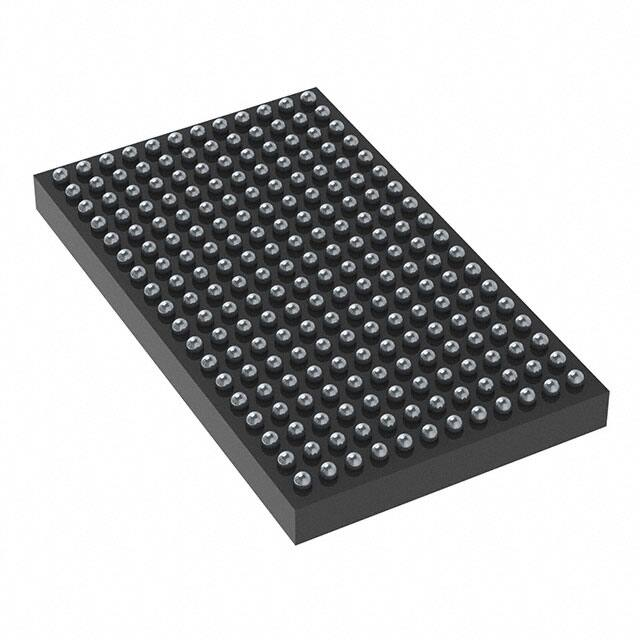


 工商网监
湘ICP备2023018690号
工商网监
湘ICP备2023018690号

