Product
Folder
Order
Now
Support &
Community
Tools &
Software
Technical
Documents
TXS0108E
SCES642F – DECEMBER 2007 – REVISED JANUARY 2019
TXS0108E 8-Bit Bi-directional, Level-Shifting, Voltage Translator
for Open-Drain and Push-Pull Applications
1 Features
3 Description
•
•
This 8-bit non-inverting translator uses two separate
configurable power-supply rails. The A port tracks the
VCCA pin supply voltage. The VCCA pin accepts any
supply voltage between 1.2 V and 3.6 V. The B port
tracks the VCCB pin supply voltage. The VCCB pin
accepts any supply voltage between 1.65 V and 5.5
V. Two input supply pins allows for low Voltage
bidirectional translation between any of the 1.2 V, 1.8
V, 2.5 V, 3.3 V, and 5 V voltage nodes.
1
•
•
•
•
•
No Direction-Control Signal Needed
Maximum Data Rates
– 110 Mbps (Push Pull)
– 1.2 Mbps (Open Drain)
1.2 V to 3.6 V on A Port and 1.65 V to 5.5 V on B
Port (VCCA ≤ VCCB)
No Power-Supply Sequencing Required – Either
VCCA or VCCB Can Be Ramped First
Latch-Up Performance Exceeds 100 mA Per
JESD 78, Class II
ESD Protection Exceeds JESD 22 (A Port)
– 2000 V Human Body Model (A114-B)
– 150 V Machine Model (A115-A)
– 1000 V Charged-Device Model (C101)
IEC 61000-4-2 ESD (B Port)
– ±8 kV Contact Discharge
– ±6 kV Air-Gap Discharge
When the output-enable (OE) input is low, all outputs
are placed in the high-impedance (Hi-Z) state.
To ensure the
down periods,
resistor. The
determined by
driver.
Device Information(1)
PART NUMBER
2 Applications
•
•
•
•
Hi-Z state during power-up or powertie OE to GND through a pull-down
minimum value of the resistor is
the current-sourcing capability of the
Handsets
Smartphones
Tablets
Desktop PCs
PACKAGE
BODY SIZE (NOM)
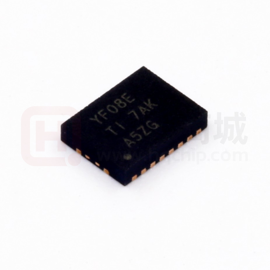
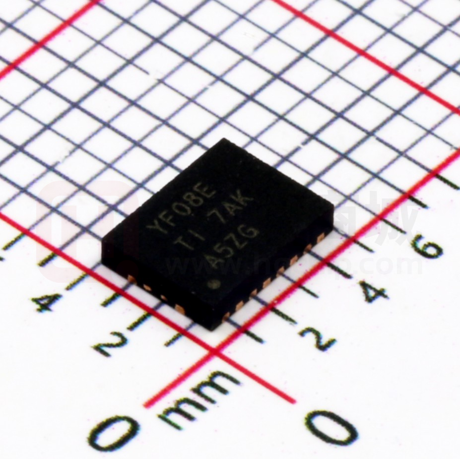
TXS0108EPW
TSSOP (20)
6.50 mm × 6.40 mm
TXS0108ERGY
VQFN (20)
4.50 mm × 3.50 mm
TXS0108EZXY
UFBGA (20)
3.00 mm × 2.50 mm
(1) For all available packages, see the orderable addendum at
the end of the datasheet.
Simplified Application
1.8 V
3.3 V
0.1 PF
0.1 PF
OE
VCCA
VCCB
1.8-V
System
Controller
Data
3.3-V
System
Controller
A1
A2
A3
A4
A5
A6
A7
A8
TXS0108E
GND
B1
B2
B3
B4
B5
B6
B7
B8
1
An IMPORTANT NOTICE at the end of this data sheet addresses availability, warranty, changes, use in safety-critical applications,
intellectual property matters and other important disclaimers. PRODUCTION DATA.
�TXS0108E
SCES642F – DECEMBER 2007 – REVISED JANUARY 2019
www.ti.com
Table of Contents
1
2
3
4
5
6
Features ..................................................................
Applications ...........................................................
Description .............................................................
Revision History.....................................................
Pin Configuration and Functions .........................
Specifications.........................................................
1
1
1
2
3
5
6.1
6.2
6.3
6.4
6.5
6.6
6.7
6.8
6.9
6.10
6.11
6.12
6.13
6.14
6.15
6.16
Absolute Maximum Ratings ..................................... 5
ESD Ratings.............................................................. 5
Recommended Operating Conditions ...................... 6
Thermal Information .................................................. 6
Electrical Characteristics: TA = –40°C to 85°C ........ 7
Timing Requirements: VCCA = 1.2 V ........................ 8
Timing Requirements: VCCA = 1.5 V ± 0.1 V ............ 8
Timing Requirements: VCCA = 1.8 V ± 0.15 V .......... 8
Timing Requirements: VCCA = 2.5 V ± 0.2 V ............ 8
Timing Requirements: VCCA = 3.3 V ± 0.3 V .......... 8
Switching Characteristics: VCCA = 1.2 V ................. 9
Switching Characteristics: VCCA = 1.5 V ± 0.1 V .. 10
Switching Characteristics: VCCA = 1.8 V ± 0.15 V 11
Switching Characteristics: VCCA = 2.5 V ± 0.2 V .. 12
Switching Characteristics: VCCA = 3.3 V ± 0.3 V .. 13
Operating Characteristics: VCCA = 1.2 V to 1.5 V,
VCCB = 1.2V to 1.5 V................................................ 14
6.17 Operating Characteristics: VCCA = 1.8 V to 3.3 V,
VCCB = 1.8 V to 3.3 V............................................... 14
7
8
Typical Characteristics........................................ 15
Parameter Measurement Information ................ 16
8.1 Load Circuits ........................................................... 16
8.2 Voltage Waveforms................................................. 17
9
Detailed Description ............................................ 18
9.1
9.2
9.3
9.4
Overview .................................................................
Functional Block Diagram .......................................
Feature Description.................................................
Device Functional Modes........................................
18
18
19
20
10 Application and Implementation........................ 21
10.1 Application Information.......................................... 21
10.2 Typical Application ............................................... 21
11 Power Supply Recommendations ..................... 23
12 Layout................................................................... 23
12.1 Layout Guidelines ................................................. 23
12.2 Layout Example .................................................... 23
13 Device and Documentation Support ................. 24
13.1
13.2
13.3
13.4
Community Resources..........................................
Trademarks ...........................................................
Electrostatic Discharge Caution ............................
Glossary ................................................................
24
24
24
24
14 Mechanical, Packaging, and Orderable
Information ........................................................... 24
4 Revision History
Changes from Revision E (February 2018) to Revision F
•
Changed TA from 125°C to 85°C in the Recommended Operating Conditions table............................................................. 6
Changes from Revision D (February 2016) to Revision E
•
2
Page
Made changes to ESD Ratings .............................................................................................................................................. 1
Changes from Revision B (November 2013) to Revision C
•
Page
Added junction temperature .................................................................................................................................................. 5
Changes from Revision C (December 2014) to Revision D
•
Page
Page
Added Pin Configuration and Functions section, ESD Ratings table, Feature Description section, Device Functional
Modes, Application and Implementation section, Power Supply Recommendations section, Layout section, Device
and Documentation Support section, and Mechanical, Packaging, and Orderable Information section .............................. 1
Submit Documentation Feedback
Copyright © 2007–2019, Texas Instruments Incorporated
Product Folder Links: TXS0108E
�TXS0108E
www.ti.com
SCES642F – DECEMBER 2007 – REVISED JANUARY 2019
5 Pin Configuration and Functions
ZXY PACKAGE
20 BUMP
(BOTTOM VIEW)
3
4
5
D
VCCA
A2
A3
A4
A5
A6
A7
A8
C
B
A
B1
2
A1
1
RGY PACKAGE
20 PINS
(TOP VIEW)
1
20
2
19
3
18
4
5
6
7
A1
VCCA
1
20
2
19
A2
A3
A4
A5
A6
A7
A8
OE
3
18
4
17
5
16
6
15
7
14
8
13
9
12
10
11
16
15
14
13
8
12
9
11
OE
GND
10
PW PACKAGE
20-PIN TSSOP
(TOP VIEW)
17
Exposed
Center
Pad
VCCB
B2
B3
B4
B5
B6
B7
B8
The exposed center pad, if used, must be
connected as a secondary ground or left
electrically open.
B1
VCCB
B2
B3
B4
B5
B6
B7
B8
GND
Table 1. Pin Assignments
1
2
3
4
5
D
VCCB
B2
B4
B6
B8
C
B1
B3
B5
B7
GND
B
A1
A3
A5
A7
OE
A
VCCA
A2
A4
A6
A8
Submit Documentation Feedback
Copyright © 2007–2019, Texas Instruments Incorporated
Product Folder Links: TXS0108E
3
�TXS0108E
SCES642F – DECEMBER 2007 – REVISED JANUARY 2019
www.ti.com
Pin Functions
PIN NO.
NAME
TYPE (1)
DESCRIPTION
PW, RGY
ZXY
A1
1
B1
I/O
Input/output 1. Referenced to VCCA
A2
3
A2
I/O
Input/output 2. Referenced to VCCA
A3
4
B2
I/O
Input/output 3. Referenced to VCCA
A4
5
A3
I/O
Input/output 4. Referenced to VCCA
A5
6
B3
I/O
Input/output 5. Referenced to VCCA
A6
7
A4
I/O
Input/output 6. Referenced to VCCA
A7
8
B4
I/O
Input/output 7. Referenced to VCCA
A8
9
A5
I/O
Input/output 8. Referenced to VCCA
B1
20
C1
I/O
Input/output 1. Referenced to VCCB
B2
18
D2
I/O
Input/output 2. Referenced to VCCB
B3
17
C2
I/O
Input/output 3. Referenced to VCCB
B4
16
D3
I/O
Input/output 4. Referenced to VCCB
B5
15
C3
I/O
Input/output 5. Referenced to VCCB
B6
14
D4
I/O
Input/output 6. Referenced to VCCB
B7
13
C4
I/O
Input/output 7. Referenced to VCCB
B8
12
D5
I/O
Input/output 8. Referenced to VCCB
GND
11
C5
—
Ground
OE
10
B5
I
Tri-state output-mode enable. Pull OE low to place all outputs in 3-state mode.
Referenced to VCCA.
VCCA
2
A1
P
A-port supply voltage. 1.2 V ≤ VCCA ≤ 3.6 V, VCCA ≤ VCCB.
VCCB
19
D1
P
B-port supply voltage. 1.65 V ≤ VCCB ≤ 5.5 V.
—
For the RGY package, the exposed center thermal pad must be either be connected to
Ground or left electrically opened.
Thermal Pad
(1)
4
I = input, O = output, I/O = input and output, P = power
Submit Documentation Feedback
Copyright © 2007–2019, Texas Instruments Incorporated
Product Folder Links: TXS0108E
�TXS0108E
www.ti.com
SCES642F – DECEMBER 2007 – REVISED JANUARY 2019
6 Specifications
6.1 Absolute Maximum Ratings (1)
over operating free-air temperature range (unless otherwise noted)
MIN
Supply voltage, VCCA
Supply voltage, VCCB
Input voltage, VI (2)
Voltage applied to any output
in the high-impedance or power-off state, VO (2)
Voltage applied to any output in the high or low state, VO (2)
(3)
MAX
4.6
V
V
–0.5
5.5
A port
–0.5
4.6
B port
–0.5
6.5
A port
–0.5
4.6
B port
–0.5
6.5
A port
–0.5
VCCA + 0.5
B port
–0.5
VCCB + 0.5
Input clamp current, IIK
VI < 0
Output clamp current, IOK
VO < 0
Continuous output current, IO
Continuous current through VCCA, VCCB, or GND
Storage temperature, Tstg
(2)
(3)
V
V
V
V
–50
mA
–50
mA
–50
50
mA
–100
100
mA
150
°C
150
°C
Junction temperature, TJ
(1)
UNIT
–0.5
–65
Stresses beyond those listed under Absolute Maximum Ratings may cause permanent damage to the device. These are stress ratings
only, and functional operation of the device at these or any other conditions beyond those indicated under Recommended Operating
Conditions is not implied. Exposure to absolute-maximum-rated conditions for extended periods may affect device reliability.
The input and output negative Voltage ratings may be exceeded if the input and output current ratings are observed.
The value of VCCA and VCCB are provided in the recommended operating conditions table.
6.2 ESD Ratings
VALUE
V(ESD)
(1)
(2)
Electrostatic
discharge
Human body model (HBM), per ANSI/ESDA/JEDEC JS-001 (1)
±2000
Charged-device model (CDM), per JEDEC specification JESD22-C101 (2)
±1000
Machine model (MM)
±150
IEC 61000-4-2 ESD (B Port) Contact Discharge
±8000
IEC 61000-4-2 ESD (B Port) Air-Gap Discharge
±6000
UNIT
V
JEDEC document JEP155 states that 500 V HBM allows safe manufacturing with a standard ESD control process.
JEDEC document JEP157 states that 250 V CDM allows safe manufacturing with a standard ESD control process.
Submit Documentation Feedback
Copyright © 2007–2019, Texas Instruments Incorporated
Product Folder Links: TXS0108E
5
�TXS0108E
SCES642F – DECEMBER 2007 – REVISED JANUARY 2019
www.ti.com
6.3 Recommended Operating Conditions
over operating free-air temperature range (unless otherwise noted) (1) (2)
MIN
MAX
UNIT
VCCA
Supply voltage
(3)
1.2
3.6
V
VCCB
Supply voltage (3)
1.65
5.5
V
VCCA (V) = 1.2 to 1.95
VCCB (V) = 1.65 to 5.5
VCCI – 0.2
VCCI
VCCA (V) = 1.95 to 3.6
VCCB (V) = 1.65 to 5.5
VCCI – 0.4
VCCI
B-Port I/Os
VCCA (V) = 1.2 to 3.6
VCCB (V) = 1.65 to 5.5
VCCI – 0.4
VCCI
V
OE
VCCA (V) = 1.2 to 3.6
VCCB (V) = 1.65 to 5.5
VCCA × 0.65
5.5
V
VCCA (V) = 1.2 to 1.95
VCCB (V) = 1.65 to 5.5
0
0.15
VCCA (V) = 1.95 to 3.6
VCCB (V) = 1.65 to 5.5
0
0.15
B-Port I/Os
VCCA (V) = 1.2 to 3.6
VCCB (V) = 1.65 to 5.5
0
0.15
V
OE
VCCA (V) = 1.2 to 3.6
VCCB (V) = 1.65 to 5.5
0
VCCA × 0.35
V
A-Port I/Os
Push-pull
VCCA (V) = 1.2 to 3.6
VCCB (V) = 1.65 to 5.5
10
ns/V
B-Port I/Os
Push-pull
VCCA (V) = 1.2 to 3.6
VCCB (V) = 1.65 to 5.5
10
ns/V
Control
input
VCCA (V) = 1.2 to 3.6
VCCB (V) = 1.65 to 5.5
10
ns/V
85
°C
A-Port I/Os
High-level input
voltage
VIH
A-Port I/Os
Low-level input
voltage
VIL
Input transition
rise or fall rate
Δt/Δv
TA
(1)
(2)
(3)
Operating free-air temperature
–40
V
V
VCCI is the VCC associated with the data input port.
VCCO is the VCC associated with the output port.
VCCA must be less than or equal to VCCB, and VCCA must not exceed 3.6 V.
6.4 Thermal Information
TXS0108E
THERMAL METRIC
(1)
PW
(TSSOP)
RGY
ZXY
UNIT
20 PINS
20 PINS
20 PINS
RθJA
Junction-to-ambient thermal resistance
101.5
34.7
101.5
°C/W
RθJC(top)
Junction-to-case (top) thermal resistance
35.9
39.5
35.9
°C/W
RθJB
Junction-to-board thermal resistance
52.4
12.7
52.4
°C/W
ψJT
Junction-to-top characterization parameter
2.3
0.9
2.3
°C/W
ψJB
Junction-to-board characterization parameter
51.9
12.7
51.9
°C/W
RθJC(bot)
Junction-to-case (bottom) thermal resistance
—
7.5
—
°C/W
(1)
6
For more information about traditional and new thermal metrics, see the IC Package Thermal Metrics application report.
Submit Documentation Feedback
Copyright © 2007–2019, Texas Instruments Incorporated
Product Folder Links: TXS0108E
�TXS0108E
www.ti.com
SCES642F – DECEMBER 2007 – REVISED JANUARY 2019
6.5 Electrical Characteristics: TA = –40°C to 85°C (1) (2) (3)
over recommended operating free-air temperature range (unless otherwise noted)
TEST
CONDITIONS
PARAMETER
VOHA
Port A output
high voltage
Port A output
low voltage
VOLA
VOHB
Port B output
high voltage
TA = 25°C
TA = –40°C to 85°C
VCCA (V)
VCCB (V)
IOH = –20 μA
VIB ≥ VCCB – 0.4 V
1.2
1.65 to 5.5
IOL = 135 μA, VIB ≤ 0.15 V
1.2
1.65 to 5.5
IOL = 180 μA, VIB ≤ 0.15 V
1.4
1.65 to 5.5
0.4
IOL = 220 μA, VIB ≤ 0.15 V
1.65
1.65 to 5.5
0.4
IOL = 300 μA, VIB ≤ 0.15 V
2.3
1.65 to 5.5
0.4
IOL = 400 μA, VIB ≤ 0.15 V
3
1.65 to 5.5
0.55
1.2
1.65 to 5.5
IOL = 220 μA, VIA ≤ 0.15 V
1.2 to 3.6
1.65
0.4
IOL = 300 μA, VIA ≤ 0.15 V
1.2 to 3.6
2.3
0.4
IOL = 400 μA, VIA ≤ 0.15 V
1.2 to 3.6
3
0.55
IOL = 620 μA, VIA ≤ 0.15 V
0.55
IOH = –20 μA,
VIA ≥ VCCA – 0.2 V
MIN
TYP
MAX
0.25
VCCB × 0.67
1.2 to 3.6
4.5
II
OE:
VI = VCCI or GND
1.2
1.65 to 5.5
–1
1
IOZ
Highimpedance
state output
current
A or B port
1.2
1.65 to 5.5
–1
1
ICCA
VCCA supply
current
VI = VO = Open, IO = 0
1.5
μA
–2
2
μA
–2
2
1.2
1.65 to 5.5
2.3 to 5.5
2
3.6
0
2
0
5.5
1.2
1.65 to 5.5
1.5 to 3.6
2.3 to 5.5
6
3.6
0
–1
0
5.5
2.3 to 5.5
1.5 to 3.6
2.3 to 5.5
V
2
1.5 to 3.6
1.2
V
V
Input leakage
current
VCCB supply
current
UNIT
V
Port B output
low voltage
ICCB
MAX
VCCA × 0.67
VOLB
VI = VO = Open, IO = 0
MIN
μA
–1
1.5
μA
1.2
3
μA
ICCA +
ICCB
Combined
supply current
VI = VCCI or GND,
IO = 0
ICCZA
Highimpedance
state VCCA
supply current
VI = VO = Open,
IO = 0, OE = GND
1.2
1.65 to 5.5
0.05
μA
ICCZB
Highimpedance
state VCCB
supply current
VI = VO = Open,
IO = 0, OE = GND
1.2
1.65 to 5.5
4
μA
Ci
Input
capacitance
OE
3.3
3.3
4.5
5.5
Input-to-output
internal
capacitance
A port
3.3
3.3
6
7
Cio
B port
3.3
3.3
5.5
6
(1)
(2)
(3)
8
pF
pF
VCCO is the VCC associated with the output port.
VCCI is the VCC associated with the input port.
VCCA must be less than or equal to VCCB, and VCCA must not exceed 3.6 V.
Submit Documentation Feedback
Copyright © 2007–2019, Texas Instruments Incorporated
Product Folder Links: TXS0108E
7
�TXS0108E
SCES642F – DECEMBER 2007 – REVISED JANUARY 2019
www.ti.com
6.6 Timing Requirements: VCCA = 1.2 V
TA = 25°C, VCCA = 1.2 V
VCCB (V)
Data rate
tw
Pulse
duration
1.8 (TYP)
2.5 (TYP)
3.3 (TYP)
5 (TYP)
Push-pull
20
20
20
20
Open-drain
2
2
2
2
Push-pull
50
50
50
50
Open-drain
500
500
500
500
Data inputs
UNIT
Mbps
ns
6.7 Timing Requirements: VCCA = 1.5 V ± 0.1 V
over recommended operating free-air temperature range, VCCA = 1.5 V ± 0.1 V (unless otherwise noted)
VCC B = 1.8 V
± 0.15 V
MIN
Data rate
Pulse
duration
Push-pull
Open-drain
MIN
VCC B= 5 V
± 0.5 V
MAX
MIN
UNIT
MIN MAX
40
60
60
50
2
2
2
2
Push-pull
Data inputs
VCC B= 3.3 V
± 0.3 V
MAX
Open-drain
tw
VCC B = 2.5 V
± 0.2 V
25
16.7
16.7
20
500
500
500
500
MAX
Mbps
ns
6.8 Timing Requirements: VCCA = 1.8 V ± 0.15 V
over recommended operating free-air temperature range, VCCA = 1.8 V ± 0.15 V (unless otherwise noted)
VCC B = 1.8 V
± 0.15 V
MIN
Data rate
tw
Pulse
duration
Push-pull
MAX
Push-pull
Open-drain
MIN
VCC B= 3.3 V
± 0.3 V
VCC B= 5 V
± 0.5 V
MIN
UNIT
MAX
MIN MAX
40
60
60
60
2
2
2
2
Open-drain
Data inputs
VCC B = 2.5 V
± 0.2 V
25
16.7
16.7
16.7
500
500
500
500
MAX
Mbps
ns
6.9 Timing Requirements: VCCA = 2.5 V ± 0.2 V
over recommended operating free-air temperature range, VCCA = 2.5 V ± 0.2 V (unless otherwise noted)
VCCB = 2.5 V
± 0.2 V
MIN
Data rate
tw
Pulse duration
Push-pull
VCCB = 3.3 V
± 0.3 V
MAX
MAX
MIN
UNIT
MAX
60
60
60
2
2
2
Open-drain
Data inputs
MIN
VCC = 5 V
± 0.5 V
Push-pull
16.7
16.7
16.7
Open-drain
500
500
500
Mbps
ns
6.10 Timing Requirements: VCCA = 3.3 V ± 0.3 V
over recommended operating free-air temperature range, VCCA = 3.3 V ± 0.3 V (unless otherwise noted)
VCCB = 3.3 V
± 0.3 V
MIN
Data rate
tw
8
Pulse duration
Push-pull
Open-drain
Data inputs
VCC = 5 V
± 0.5 V
MAX
MIN
60
60
2
2
Push-pull
16.7
16.7
Open-drain
500
500
Submit Documentation Feedback
UNIT
MAX
Mbps
ns
Copyright © 2007–2019, Texas Instruments Incorporated
Product Folder Links: TXS0108E
�TXS0108E
www.ti.com
SCES642F – DECEMBER 2007 – REVISED JANUARY 2019
6.11 Switching Characteristics: VCCA = 1.2 V
over operating free-air temperature range (unless otherwise noted)
PARAMETER
VCCB = 1.8 V
± 0.15 V
TEST CONDITIONS
MIN
TYP
MAX
VCCB = 2.5 V
± 0.2 V
MIN
TYP
MAX
VCCB = 3.3 V
± 0.3 V
MIN
TYP
MAX
VCCB = 5 V
± 0.5 V
MIN
TYP
Push-pull
driving
6.5
5.9
5.7
5.5
tPHL
Propagation
delay time
A-to-B
(high-to-low
output)
Open-drain
driving
11.9
11.1
11
11.1
Push-pull
driving
7.1
6.3
6.2
6.6
tPLH
Propagation
delay time
A-to-B
(low-to-high
output)
Open-drain
driving
293
236
197
152
Push-pull
driving
6.4
6
5.8
5.6
tPHL
Propagation
delay time
B-to-A
(high-to-low
output)
Open-drain
driving
8.5
6.8
6.2
5.9
Push-pull
driving
5.6
4.1
3.6
3.2
tPLH
Propagation
delay time
B-to-A
(low-to-high
output)
Open-drain
driving
312
248
192
132
ten
Enable time
OE-to-A or B
Push-pull
driving
200
200
200
200
tdis
Disable
time
OE-to-A or B
Push-pull
driving
16.8
13.9
13.2
13.5
6.7
6.5
6.4
Input rise
time
A-port
rise time
Push-pull
driving
7.9
trA
Open-drain
driving
296
238
185
127
3.3
1.8
1.5
Input rise
time
B-port
rise time
Push-pull
driving
6.3
trB
Open-drain
driving
236
164
115
60
4.8
4.3
3.8
Input fall
time
A-port
fall time
Push-pull
driving
5.8
tfA
Open-drain
driving
5.9
4.7
4.1
3.5
Push-pull
driving
4.6
2.8
2.2
1.9
Open-drain
driving
4.5
2.7
2.2
1.9
1
1
1
1
tfB
Input fall
time
B-port
fall time
tSK(O)
Skew
(time),
output
Channel
-tochannel
skew
Maximum
data rate
A or B
UNIT
MAX
ns
ns
ns
ns
ns
ns
ns
Push-pull
driving
ns
Push-pull
driving
20
20
20
20
Open-drain
driving
2
2
2
2
Mbps
Submit Documentation Feedback
Copyright © 2007–2019, Texas Instruments Incorporated
Product Folder Links: TXS0108E
9
�TXS0108E
SCES642F – DECEMBER 2007 – REVISED JANUARY 2019
www.ti.com
6.12 Switching Characteristics: VCCA = 1.5 V ± 0.1 V
over recommended operating free-air temperature range, VCCA = 1.5 V ± 0.1 V (unless otherwise noted)
PARAMETER
VCCB = 1.8 V
± 0.15 V
TEST CONDITIONS
VCCB = 2.5 V
± 0.2 V
MIN
MAX
4
14.4
Push-pull driving
VCCB = 3.3 V
± 0.3 V
MIN
MAX
3.6
12.8
MIN
MAX
3.5
12.2
A-to-B
tPLH
Propagation
delay time
(low-to-high output)
A-to-B
tPHL
Propagation
delay time
(high-to-low output)
B-to-A
tPLH
Propagation
delay time
(low-to-high output)
B-to-A
ten
Enable time
OE-to-A or B
Push-pull driving
200
200
200
200
ns
tdis
Disable time
OE-to-A or B
Push-pull driving
28.1
22
20.1
19.6
ns
Open-drain driving
A-port rise time
trB
Input rise time
B-port rise time
tfA
Input fall time
A-port fall time
tfB
Input fall time
B-port fall time
Skew (time), output
Channel-tochannel skew
Maximum
data rate
A or B
Open-drain driving
720
10
143
12.7
3.4
Push-pull driving
Input rise time
10
182
Push-pull driving
trA
tSK(O)
Open-drain driving
12
745
554
3.1
9.6
114
473
2.8
8.5
603
81
384
2.5
7.5
519
1.6
84
3.5
13.1
3
9.8
3.1
9
3.2
8.3
Open-drain driving
147
982
115
716
92
592
66
481
Push-pull driving
2.9
11.4
1.9
7.4
0.9
4.7
0.7
2.6
Open-drain driving
135
1020
91
756
58
653
20
370
Push-pull driving
2.3
9.9
1.7
7.7
1.6
6.8
1.7
6
Open-drain driving
2.4
10
2.1
7.9
1.7
7
1.5
6.2
2
8.7
1.3
5.5
0.9
3.8
0.8
3.1
1.2
11.5
1.3
8.6
1
9.6
0.5
7.7
1
1
1
Open-drain driving
Push-pull driving
Push-pull driving
Open-drain driving
1.1
1
40
60
60
50
2
2
2
2
Submit Documentation Feedback
ns
407
Push-pull driving
Push-pull driving
ns
12
5.1
118
12
9.7
11
6.2
147
8.6
3.5
9.8
11.1
13.2
9.5
186
8.6
UNIT
MAX
Propagation
delay time
(high-to-low output)
Push-pull driving
9.2
MIN
tPHL
Open-drain driving
11
VCCB = 5 V
± 0.5 V
ns
ns
ns
ns
Mbps
Copyright © 2007–2019, Texas Instruments Incorporated
Product Folder Links: TXS0108E
�TXS0108E
www.ti.com
SCES642F – DECEMBER 2007 – REVISED JANUARY 2019
6.13 Switching Characteristics: VCCA = 1.8 V ± 0.15 V
over recommended operating free-air temperature range, VCCA = 1.8 V ± 0.15 V (unless otherwise noted)
PARA-METER
TEST CONDITIONS
VCCB = 1.8 V
± 0.15 V
MIN
Push-pull
driving
VCCB = 2.5 V
± 0.2 V
MAX
MIN
VCCB = 3.3 V
± 0.3 V
MAX
8.2
MIN
6.4
VCCB = 5 V
± 0.5 V
MAX
MIN
5.7
UNIT
MAX
5.6
tPHL
Propagation
delay time
(high-to-low
output)
tPLH
Propagation
delay time
(low-to-high
output)
tPHL
Propagation
delay time
(high-to-low
output)
tPLH
Propagation
delay time
(low-to-high
output)
B-to-A
ten
Enable time
OE-to-A or B
Push-pull
driving
200
200
200
200
tdis
Disable time
OE-to-A or B
Push-pull
driving
25.1
18.8
16.5
15.3
trA
Input rise time
A-port rise time
trB
Input rise time
B-port rise time
tfA
Input fall time
A-port fall time
A-to-B
A-to-B
B-to-A
tfB
Input fall time
B-port fall time
tSK(O)
Skew (time),
output
Channel-tochannel skew
Maximum
data rate
A or B
Open-drain
driving
3.6
Push-pull
driving
Open-drain
driving
194
729
3.4
12.1
155
733
3.1
584
2.8
8.5
126
578
3.1
466
2.5
7.3
90
459
346
2.1
6.2
5
93
3.1
11.9
2.6
8.6
2.7
7.8
2.8
7.2
Open-drain
driving
155
996
124
691
100
508
72
350
Push-pull
driving
2.8
10.5
1.8
7.2
1.2
5.2
0.7
2.7
Open-drain
driving
132
1001
106
677
73
546
32
323
Push-pull
driving
2.1
8.8
1.6
6.6
1.4
5.7
1.4
4.9
Open-drain
driving
2.2
9
1.7
6.7
1.4
5.8
1.2
5.2
2
8.3
1.3
5.4
0.9
3.9
0.7
3
0.8
10.5
0.7
10.7
1
9.6
0.6
7.8
Open-drain
driving
Push-pull
driving
Push-pull
driving
Open-drain
driving
1
1
1
1
40
60
60
60
2
2
2
2
Submit Documentation Feedback
Copyright © 2007–2019, Texas Instruments Incorporated
Product Folder Links: TXS0108E
ns
323
Push-pull
driving
Push-pull
driving
ns
7
5.8
129
8.9
6.3
7.4
7
159
9.3
6.5
8
10.2
197
9.9
2.1
9.8
Push-pull
driving
Open-drain
driving
3.2
9
Push-pull
driving
Open-drain
driving
11.4
ns
ns
ns
ns
ns
ns
Mbps
11
�TXS0108E
SCES642F – DECEMBER 2007 – REVISED JANUARY 2019
www.ti.com
6.14 Switching Characteristics: VCCA = 2.5 V ± 0.2 V
over recommended operating free-air temperature range, VCCA = 2.5 V ± 0.2 V (unless otherwise noted)
PARA-METER
VCCB = 2.5 V
± 0.2 V
TEST CONDITIONS
MIN
Push-pull
driving
VCCB = 3.3 V
± 0.3 V
MAX
MIN
5
VCCB = 5 V
± 0.5 V
MAX
MIN
4
UNIT
MAX
3.7
tPHL
Propagation
delay time
(high-to-low
output)
tPLH
Propagation
delay time
(low-to-high
output)
tPHL
Propagation
delay time
(high-to-low
output)
tPLH
Propagation
delay time
(low-to-high
output)
B-to-A
ten
Enable time
OE-to-A or B
Push-pull
driving
200
200
200
tdis
Disable time
OE-to-A or B
Push-pull
driving
15.7
12.9
11.2
trA
Input rise time
A-port rise time
trB
tfA
Input rise time
Input fall time
A -to-B
A -to-B
B-to-A
B-port rise time
A-port fall time
tfB
Input fall time
B-port fall time
tSK(O)
Skew (time),
output
Channel-tochannel skew
Maximum
data rate
A or B
12
Open-drain
driving
2.4
Push-pull
driving
6.9
2.3
5.2
Open-drain
driving
149
Push-pull
driving
592
2.5
Push-pull
driving
7.3
125
Push-pull
driving
150
595
488
2.2
6
93
481
368
1.8
4.9
3.5
94
7.3
2.1
6.4
2.2
5.8
Open-drain
driving
110
692
93
529
68
369
Push-pull
driving
1.8
6.5
1.3
5.1
0.7
3.4
Open-drain
driving
107
693
79
483
41
304
Push-pull
driving
1.5
5.7
1.2
4.7
1.3
3.8
Open-drain
driving
1.5
5.6
1.2
4.7
1.1
4
Push-pull
driving
1.4
5.4
0.9
4.1
0.7
3
Open-drain
driving
0.4
14.2
0.5
19.4
0.4
3
1
Push-pull
driving
Open-drain
driving
1.2
1
60
60
60
2
2
2
Submit Documentation Feedback
ns
345
2
Push-pull
driving
ns
4.2
4.4
126
5.8
3.9
4.7
5.9
Open-drain
driving
2.2
4.3
5.4
Open-drain
driving
6.3
ns
ns
ns
ns
ns
ns
Mbps
Copyright © 2007–2019, Texas Instruments Incorporated
Product Folder Links: TXS0108E
�TXS0108E
www.ti.com
SCES642F – DECEMBER 2007 – REVISED JANUARY 2019
6.15 Switching Characteristics: VCCA = 3.3 V ± 0.3 V
over recommended operating free-air temperature range, VCCA = 3.3 V ± 0.3 V (unless otherwise noted)
PARAMETER
TEST CONDITIONS
VCCB = 3.3 V
± 0.3 V
MIN
Push-pull driving
VCCB = 5 V
± 0.5 V
MAX
MIN
tPHL
Propagation
delay time
(high-to-low output)
A-to-B
tPLH
Propagation
delay time
(low-to-high output)
A-to-B
tPHL
Propagation
delay time
(high-to-low output)
B-to-A
tPLH
Propagation
delay time
(low-to-high output)
A-to-B
ten
Enable time
OE-to-A or B
Push-pull driving
200
200
ns
tdis
Disable time
OE-to-A or B
Push-pull driving
11.9
9.8
ns
Open-drain driving
Open-drain driving
Open-drain driving
111
A-port rise time
trB
Input rise time
B-port rise time
tfA
Input fall time
A-port fall time
Input fall time
B-port fall time
Skew (time), output
Channel-tochannel skew
Maximum data rate
A or B
3.1
1.9
439
5.5
87
449
352
4.5
4.3
86
1.8
5.7
1.9
5
Open-drain driving
75
446
57
337
Push-pull driving
1.5
5
1
3.6
Open-drain driving
72
427
40
290
Push-pull driving
1.2
4.5
1.1
3.5
Open-drain driving
1.1
4.4
1
3.7
Push-pull driving
1.1
4.2
0.8
3.1
1
4.2
0.8
3.1
1
Push-pull driving
Push-pull driving
1
60
60
2
2
Open-drain driving
Submit Documentation Feedback
Copyright © 2007–2019, Texas Instruments Incorporated
Product Folder Links: TXS0108E
ns
339
Push-pull driving
Open-drain driving
ns
3.8
1.7
3.8
112
4.8
3.5
4.2
2.1
Push-pull driving
Open-drain driving
5.3
3.9
Push-pull driving
Input rise time
tSK(O)
2
Push-pull driving
trA
tfB
3.8
UNIT
MAX
ns
ns
ns
ns
Mbps
13
�TXS0108E
SCES642F – DECEMBER 2007 – REVISED JANUARY 2019
www.ti.com
6.16 Operating Characteristics: VCCA = 1.2 V to 1.5 V, VCCB = 1.2V to 1.5 V
TA = 25°C
PARAMETER
CpdA
Power
dissipation
capacitance
CpdB
Power
dissipation
capacitance
CpdA
Power
dissipation
capacitance
CpdB
Power
dissipation
capacitance
VCCA = 1.2 V, VCCB = 1.2 V
TEST CONDITIONS
CL = 0
f = 10 MHz
tr= tf= 1 ns
OE = VCCA
(outputs
enabled)
CL = 0
f = 10 MHz
tr= tf= 1 ns
OE = VCCA
(outputs
enabled)
MIN
TYP
VCCA = 1.2 V, VCCB = 1.2 V
MAX
MIN
TYP
VCCA = 1.5 V, VCCB = 1.5 V
MAX
MIN
TYP
A-port input,
B-port output
5.9
5.7
5.9
B-port input,
A-port output
10.2
10.3
9.9
A-port input,
B-port output
29.9
22.2
21.5
B-port input,
A-port output
22.9
16.7
16.7
A-port input,
B-port output
0.01
0.01
0.01
B-port input,
A-port output
0.06
0.01
0.01
A-port input,
B-port output
0.06
0.01
0.01
B-port input,
A-port output
0.06
0.01
0.01
MAX
UNIT
pF
pF
6.17 Operating Characteristics: VCCA = 1.8 V to 3.3 V, VCCB = 1.8 V to 3.3 V
TA = 25°C
PARAMETER
TEST CONDITIONS
VCCA = 1.8 V,
VCCB = 1.8 V
MIN
CpdA
Power
dissipation
capacitance
CpdB
Power
dissipation
capacitance
CpdA
Power
dissipation
capacitance
CpdB
Power
dissipation
capacitance
14
CL = 0
f = 10 MHz
tr= tf= 1 ns
OE = VCCA
(outputs
enabled)
CL = 0
f = 10 MHz
tr= tf= 1 ns
OE = VCCA
(outputs
enabled)
TYP
MAX
VCCA = 2.5 V,
VCCB = 2.5 V
MIN
TYP
MAX
VCCA = 2.5 V,
VCCB = 2.5 V
MIN
TYP
MAX
VCCA = 3.3 V,
VCCB = 3.3 V
MIN
TYP
A-port input,
B-port output
5.9
6.7
6.9
8
B-port input,
A-port output
9.7
9.7
9.4
9.8
A-port input,
B-port output
20.8
21
23.4
23
B-port input,
A-port output
16.8
17.8
20.8
20.9
A-port input,
B-port output
0.01
0.01
0.01
0.01
B-port input,
A-port output
0.01
0.01
0.01
0.01
A-port input,
B-port output
0.01
0.01
0.03
0.02
B-port input,
A-port output
0.01
0.01
0.03
0.02
Submit Documentation Feedback
UNIT
MAX
pF
pF
Copyright © 2007–2019, Texas Instruments Incorporated
Product Folder Links: TXS0108E
�TXS0108E
www.ti.com
SCES642F – DECEMBER 2007 – REVISED JANUARY 2019
0.6
0.6
0.5
0.5
Low-Level Output Voltage (V)
Low-Level Output Voltage (V)
7 Typical Characteristics
0.4
0.3
0.2
0.1
0.4
0.3
0.2
0.1
VCCB = 5.5V
VCCB = 2.7V
0
0
0
200
VCCA = 2.3 V
400
600
Low-Level Current (µA)
800
1000
0
200
400
600
Low-Level Current µA)
D001
VIL(A) = 0.15 V
VCCA = 3.0 V
Figure 1. Low-Level Output Voltage (VOL(Bx)) vs Low-Level
Current (IOL(Bx))
800
1000
D002
VIL(A) = 0.15 V
Figure 2. Low-Level Output Voltage (VOL(Bx)) vs Low-Level
Current (IOL(Bx))
Low-Level Output Voltage (V)
0.6
0.5
0.4
0.3
0.2
0.1
VCCB = 1.95 V
VCCB = 5.5 V
0
0
100
VCCA = 1.2 V
200
300
400
Low-Level Current (µA)
500
600
D003
VIL(A) = 0.15 V
Figure 3. Low-Level Output Voltage (VOL(Bx)) vs Low-Level Current (IOL(Bx))
Submit Documentation Feedback
Copyright © 2007–2019, Texas Instruments Incorporated
Product Folder Links: TXS0108E
15
�TXS0108E
SCES642F – DECEMBER 2007 – REVISED JANUARY 2019
www.ti.com
8 Parameter Measurement Information
8.1 Load Circuits
Figure 4 shows the push-pull driver circuit used for measuring data rate, pulse duration, propagation delay,
output rise-time and fall-time. Figure 5 shows the open-drain driver circuit used for measuring data rate, pulse
duration, propagation delay, output rise-time and fall-time.
VCCI
VCCO
DUT
IN
OUT
15 pF
(1)
VCCI is the VCC associated with the input port.
(2)
VCCO is the VCC associated with the output port.
1M
Figure 4. Data Rate, Pulse Duration, Propagation Delay, Output Rise-Time And Fall-Time Measurement
Using a Push-Pull Driver
VCCI
VCCO
DUT
IN
OUT
15 pF
(1)
VCCI is the VCC associated with the input port.
(2)
VCCO is the VCC associated with the output port.
1M
Figure 5. Data Rate (10 pF), Pulse Duration (10 pF), Propagation Delay, Output Rise-Time And Fall-Time
Measurement Using an Open-Drain Driver
2 × VCCO
50 k
From Output
Under Test
15 pF
(1)
tPLZ and tPHZ are the same as tdis.
(2)
tPZL and tPZH are the same as ten.
S1
Open
50 k
TEST
S1
tPZL, tPLZ
(tdis)
2 × VCCO
tPHZ, tPZH
(ten)
Open
Figure 6. Load Circuit for Enable-Time and Disable-Time Measurement
16
Submit Documentation Feedback
Copyright © 2007–2019, Texas Instruments Incorporated
Product Folder Links: TXS0108E
�TXS0108E
www.ti.com
SCES642F – DECEMBER 2007 – REVISED JANUARY 2019
8.2 Voltage Waveforms
tw
VCCI
Input
VCCI / 2
VCCI / 2
0V
Figure 7. Pulse Duration (Push-Pull)
VCCI
Input
VCCI / 2
VCCI / 2
0V
tPLH
Output
tPHL
VCCO / 2
0.9
VCCO
0.1
VCCO
tr
VOH
VCCO / 2
VOL
tf
Figure 8. Propagation Delay Times
Submit Documentation Feedback
Copyright © 2007–2019, Texas Instruments Incorporated
Product Folder Links: TXS0108E
17
�TXS0108E
SCES642F – DECEMBER 2007 – REVISED JANUARY 2019
www.ti.com
9 Detailed Description
9.1 Overview
The TXS0108E device is a directionless voltage-level translator specifically designed for translating logic voltage
levels. The A-port accepts I/O voltages ranging from 1.2 V to 3.6 V. The B-port accepts I/O voltages from 1.65 V
to 5.5 V. The device uses pass gate architecture with edge rate accelerators (one shots) to improve the overall
data rate. The pull-up resistors, commonly used in open-drain applications, have been conveniently integrated so
that an external resistor is not needed. While this device is designed for open-drain applications, the device can
also translate push-pull CMOS logic outputs.
9.2 Functional Block Diagram
VCCB
VCCA
OE
One Shot
Accelerator
One Shot
Accelerator
Gate Bias
Rpua
Rpub
A1
B1
6 channels
One Shot
Accelerator
A2
A3
A4
A5
A6
A7
One Shot
Accelerator
Gate Bias
Rpub
Rpua
One Shot
Accelerator
B2
B3
B4
B5
B6
B7
One Shot
Accelerator
Gate Bias
Rpub
Rpua
A8
B8
Figure 9. Functional Block Diagram
Each A-port I/O has a pull-up resistor (RPUA) to VCCA and each B-port I/O has a pull-up resistor (RPUB) to VCCB.
RPUA and RPUB have a value of 40 kΩ when the output is driving low. RPUA and RPUB have a value of 4 kΩ when
the output is driving high. RPUA and RPUB are disabled when OE = Low.
18
Submit Documentation Feedback
Copyright © 2007–2019, Texas Instruments Incorporated
Product Folder Links: TXS0108E
�TXS0108E
www.ti.com
SCES642F – DECEMBER 2007 – REVISED JANUARY 2019
9.3 Feature Description
9.3.1 Architecture
Figure 10 describes semi-buffered architecture design this application requires for both push-pull and open-drain
mode. This application uses edge-rate accelerator circuitry (for both the high-to-low and low-to-high edges), a
high-on-resistance N-channel pass-gate transistor (on the order of 300 Ω to 500 Ω) and pull-up resistors (to
provide DC-bias and drive capabilities) to meet these requirements. This design needs no direction-control signal
(to control the direction of data flow from A to B or from B to A). The resulting implementation supports both lowspeed open-drain operation as well as high-speed push-pull operation.
VCCA
VCCB
RPUA
Translator
T1
A
Bias
One-Shot
Accelerator
OS3
P2
One-Shot
Accelerator
OS4
N2
R1
R2
RPUB
B
Npass
P1
N1
One-Shot
Accelerator
OS1
One-Shot
Accelerator
OS2
Translator
T2
Figure 10. Architecture of a TXS0108E Cell
When transmitting data from A-ports to B-ports, during a rising edge the one-shot circuit (OS3) turns on the
PMOS transistor (P2) for a short-duration which reduces the low-to-high transition time. Similarly, during a falling
edge, when transmitting data from A to B, the one-shot circuit (OS4) turns on the N-channel MOSFET transistor
(N2) for a short-duration which speeds up the high-to-low transition. The B-port edge-rate accelerator consists of
one-shot circuits OS3 and OS4. Transistors P2 and N2 and serves to rapidly force the B port high or low when a
corresponding transition is detected on the A port.
When transmitting data from B- to A-ports, during a rising edge the one-shot circuit (OS1) turns on the PMOS
transistor (P1) for a short-duration which reduces the low-to-high transition time. Similarly, during a falling edge,
when transmitting data from B to A, the one-shot circuit (OS2) turns on NMOS transistor (N1) for a short-duration
and this speeds up the high-to-low transition. The A-port edge-rate accelerator consists of one-shots OS1 and
OS2, transistors P1 and N1 components and form the edge-rate accelerator and serves to rapidly force the A
port high or low when a corresponding transition is detected on the B port.
Submit Documentation Feedback
Copyright © 2007–2019, Texas Instruments Incorporated
Product Folder Links: TXS0108E
19
�TXS0108E
SCES642F – DECEMBER 2007 – REVISED JANUARY 2019
www.ti.com
Feature Description (continued)
9.3.2 Input Driver Requirements
The continuous DC-current sinking capability is determined by the external system-level open-drain (or push-pull)
drivers that are interfaced to the TXS0108E I/O pins. Because the high bandwidth of these bidirectional I/O
circuits is used to facilitate this fast change from an input to an output and an output to an input, they have a
modest DC-current sourcing capability of hundreds of micro-amperes, as determined by the internal pull-up
resistors.
The fall time (tfA, tfB) of a signal depends on the edge-rate and output impedance of the external device driving
TXS0108E data I/Os, as well as the capacitive loading on the data lines.
Similarly, the tPHL and maximum data rates also depend on the output impedance of the external driver. The
values for tfA, tfB, tPHL, and maximum data rates in the data sheet assume that the output impedance of the
external driver is less than 50 Ω.
9.3.3 Output Load Considerations
TI recommends careful PCB layout practices with short PCB trace lengths to avoid excessive capacitive loading
and to ensure that proper one-shot triggering takes place. PCB signal trace-lengths should be kept short enough
such that the round trip delay of any reflection is less than the one-shot duration. This improves signal integrity
by ensuring that any reflection sees a low impedance at the driver. The one-shot circuits have been designed to
stay on for approximately 30 ns. The maximum capacitance of the lumped load that can be driven also depends
directly on the one-shot duration. With very heavy capacitive loads, the one-shot can time-out before the signal is
driven fully to the positive rail. The one-shot duration has been set to best optimize trade-offs between dynamic
ICC, load driving capability, and maximum bit-rate considerations. Both PCB trace length and connectors add to
the capacitance of the TXS0108E output. Therefore, TI recommends that this lumped-load capacitance is
considered in order to avoid one-shot retriggering, bus contention, output signal oscillations, or other adverse
system-level affects.
9.3.4 Enable and Disable
The TXS0108E has an OE pin input that is used to disable the device by setting the OE pin low, which places all
I/Os in the Hi-Z state. The disable time (tdis) indicates the delay between the time when the OE pin goes low and
when the outputs actually get disabled (Hi-Z). The enable time (ten) indicates the amount of time the design must
allow for the one-shot circuitry to become operational after the OE pin goes high.
9.3.5 Pull-up or Pull-down Resistors on I/O Lines
The TXS0108E has the smart pull-up resistors dynamically change value based on whether a low or a high is
being passed through the I/O line. Each A-port I/O has a pull-up resistor (RPUA) to VCCA and each B-port I/O has
a pull-up resistor (RPUB) to VCCB. RPUA and RPUB have a value of 40 kΩ when the output is driving low. RPUA and
RPUB have a value of 4 kΩ when the output is driving high. RPUA and RPUB are disabled when OE = Low. This
feature provides lower static power consumption (when the I/Os are passing a low), and supports lower VOL
values for the same size pass-gate transistor, and helps improve simultaneous switching performance.
9.4 Device Functional Modes
The TXS0108E device has two functional modes, enabled and disabled. To disable the device set the OE pin
input low, which places all I/Os in a high impedance state. Setting the OE pin input high enables the device.
20
Submit Documentation Feedback
Copyright © 2007–2019, Texas Instruments Incorporated
Product Folder Links: TXS0108E
�TXS0108E
www.ti.com
SCES642F – DECEMBER 2007 – REVISED JANUARY 2019
10 Application and Implementation
NOTE
Information in the following applications sections is not part of the TI component
specification, and TI does not warrant its accuracy or completeness. TI’s customers are
responsible for determining suitability of components for their purposes. Customers should
validate and test their design implementation to confirm system functionality.
10.1 Application Information
The TXS0108E can be used in level-translation applications for interfacing devices or systems operating at
different interface voltages with one another. The device is ideal for use in applications where an open-drain
driver is connected to the data I/Os. The device is appropriate for applications where a push-pull driver is
connected to the data I/Os, but the TXB0104 device, (SCES650) 4-Bit Bidirectional Voltage-Level Translator
might be a better option for such push-pull applications. The device is a semi-buffered auto-direction-sensing
voltage translator design is optimized for translation applications (for example, MMC Card Interfaces) that require
the system to start out in a low-speed open-drain mode and then switch to a higher speed push-pull mode.
10.2 Typical Application
1.8 V
3.3 V
0.1 PF
0.1 PF
VCCA
OE
VCCB
1.8-V
System
Controller
3.3-V
System
Controller
A1
A2
A3
A4
A5
A6
A7
A8
Data
TXS0108E
GND
B1
B2
B3
B4
B5
B6
B7
B8
Figure 11. Typical Application Circuit
10.2.1 Design Requirements
For this design example, use the parameters listed in Table 2. Ensure that VCCA ≤ VCCB.
Table 2. Design Parameters
DESIGN PARAMETER
EXAMPLE VALUE
Input voltage range
1.4 V to 3.6 V
Output voltage range
1.65 V to 5.5 V
10.2.2 Detailed Design Procedure
To begin the design process, determine the following:
• Input voltage range
– Use the supply voltage of the device that is driving the TXS0108E device to determine the input voltage
range. For a valid logic high the value must exceed the VIH of the input port. For a valid logic low the value
Submit Documentation Feedback
Copyright © 2007–2019, Texas Instruments Incorporated
Product Folder Links: TXS0108E
21
�TXS0108E
SCES642F – DECEMBER 2007 – REVISED JANUARY 2019
•
•
www.ti.com
must be less than the VIL of the input port.
Output voltage range
– Use the supply voltage of the device that the TXS0108E device is driving to determine the output voltage
range.
– The TXS0108E device has smart internal pull-up resistors. External pull-up resistors can be added to
reduce the total RC of a signal trace if necessary.
An external pull-down resistor decreases the output VOH and VOL. Use Equation 1 to calculate the VOH as a
result of an external pull-down resistor.
VOH = VCCx × RPD / (RPD + 4 kΩ)
(1)
10.2.3 Application Curves
VCCA = 1.8 V
VCCB = 3.3 V
Figure 12. Level-Translation of a 2.5-MHz Signal
22
Submit Documentation Feedback
Copyright © 2007–2019, Texas Instruments Incorporated
Product Folder Links: TXS0108E
�TXS0108E
www.ti.com
SCES642F – DECEMBER 2007 – REVISED JANUARY 2019
11 Power Supply Recommendations
During operation, ensure that VCCA ≤ VCCB at all times. The sequencing of each power supply will not damage the
device during the power up operation, so either power supply can be ramped up first. The output-enable (OE)
input circuit is designed so that it is supplied by VCCA and when the (OE) input is low, all outputs are placed in the
high-impedance state. To ensure the high-impedance state of the outputs during power up or power down, the
OE input pin must be tied to GND through a pull-down resistor and must not be enabled until VCCA and VCCB are
fully ramped and stable. The minimum value of the pull-down resistor to ground is determined by the currentsourcing capability of the driver.
12 Layout
12.1 Layout Guidelines
To ensure reliability of the device, following common printed-circuit board layout guidelines is recommended.
• Bypass capacitors should be used on power supplies. Place the capacitors as close as possible to the VCCA,
VCCB pin and GND pin.
• Short trace lengths should be used to avoid excessive loading.
• PCB signal trace-lengths must be kept short enough so that the round-trip delay of any reflection is less than
the one shot duration, approximately 30 ns, ensuring that any reflection encounters low impedance at the
source driver.
12.2 Layout Example
LEGEND
Polygonal Copper Pour
VIA to Power Plane
VIA to GND Plane (Inner Layer)
TXS0108EPWR
To Controller
1
A1
B1
20
Bypass capacitor 0.1
0.1 µF
µF
0.1
0.1 µF
µF Bypass capacitor
2
VCCA
VCCB
19
3
A2
B2
18
4
A3
B3
17
5
A4
B4
16
6
A5
B5
15
7
A6
B6
14
8
A7
B7
13
9
A8
B8
12
10
OE
GND
11
To system
To system
To Controller
To system
To Controller
To Controller
To Controller
To system
To system
To system
To Controller
To Controller
To system
To system
To Controller
Keep OE low until VCCA and VCCB are powered up
Figure 13. Layout Example
Submit Documentation Feedback
Copyright © 2007–2019, Texas Instruments Incorporated
Product Folder Links: TXS0108E
23
�TXS0108E
SCES642F – DECEMBER 2007 – REVISED JANUARY 2019
www.ti.com
13 Device and Documentation Support
13.1 Community Resources
The following links connect to TI community resources. Linked contents are provided "AS IS" by the respective
contributors. They do not constitute TI specifications and do not necessarily reflect TI's views; see TI's Terms of
Use.
TI E2E™ Online Community TI's Engineer-to-Engineer (E2E) Community. Created to foster collaboration
among engineers. At e2e.ti.com, you can ask questions, share knowledge, explore ideas and help
solve problems with fellow engineers.
Design Support TI's Design Support Quickly find helpful E2E forums along with design support tools and
contact information for technical support.
13.2 Trademarks
E2E is a trademark of Texas Instruments.
All other trademarks are the property of their respective owners.
13.3 Electrostatic Discharge Caution
These devices have limited built-in ESD protection. The leads should be shorted together or the device placed in conductive foam
during storage or handling to prevent electrostatic damage to the MOS gates.
13.4 Glossary
SLYZ022 — TI Glossary.
This glossary lists and explains terms, acronyms, and definitions.
14 Mechanical, Packaging, and Orderable Information
The following pages include mechanical, packaging, and orderable information. This information is the most
current data available for the designated devices. This data is subject to change without notice and revision of
this document. For browser-based versions of this data sheet, refer to the left-hand navigation.
24
Submit Documentation Feedback
Copyright © 2007–2019, Texas Instruments Incorporated
Product Folder Links: TXS0108E
�PACKAGE OPTION ADDENDUM
www.ti.com
14-Jan-2019
PACKAGING INFORMATION
Orderable Device
Status
(1)
Package Type Package Pins Package
Drawing
Qty
Eco Plan
Lead/Ball Finish
MSL Peak Temp
(2)
(6)
(3)
Op Temp (°C)
Device Marking
(4/5)
TXS0108EPWR
ACTIVE
TSSOP
PW
20
2000
Green (RoHS
& no Sb/Br)
CU NIPDAU
Level-1-260C-UNLIM
-40 to 85
YF08E
TXS0108EPWRG4
ACTIVE
TSSOP
PW
20
2000
Green (RoHS
& no Sb/Br)
CU NIPDAU
Level-1-260C-UNLIM
-40 to 85
YF08E
TXS0108ERGYR
ACTIVE
VQFN
RGY
20
3000
Green (RoHS
& no Sb/Br)
CU NIPDAU
Level-2-260C-1 YEAR
-40 to 85
YF08E
TXS0108EZXYR
ACTIVE
BGA
MICROSTAR
JUNIOR
ZXY
20
2500
Green (RoHS
& no Sb/Br)
SNAGCU
Level-1-260C-UNLIM
-40 to 85
YF08E
(1)
The marketing status values are defined as follows:
ACTIVE: Product device recommended for new designs.
LIFEBUY: TI has announced that the device will be discontinued, and a lifetime-buy period is in effect.
NRND: Not recommended for new designs. Device is in production to support existing customers, but TI does not recommend using this part in a new design.
PREVIEW: Device has been announced but is not in production. Samples may or may not be available.
OBSOLETE: TI has discontinued the production of the device.
(2)
RoHS: TI defines "RoHS" to mean semiconductor products that are compliant with the current EU RoHS requirements for all 10 RoHS substances, including the requirement that RoHS substance
do not exceed 0.1% by weight in homogeneous materials. Where designed to be soldered at high temperatures, "RoHS" products are suitable for use in specified lead-free processes. TI may
reference these types of products as "Pb-Free".
RoHS Exempt: TI defines "RoHS Exempt" to mean products that contain lead but are compliant with EU RoHS pursuant to a specific EU RoHS exemption.
Green: TI defines "Green" to mean the content of Chlorine (Cl) and Bromine (Br) based flame retardants meet JS709B low halogen requirements of


 工商网监
湘ICP备2023018690号
工商网监
湘ICP备2023018690号
