TXS0206
www.ti.com
SCES697C – AUGUST 2009 – REVISED JANUARY 2010
MMC, SD CARD, Memory Stick™ VOLTAGE-TRANSLATION TRANSCEIVER
WITH ESD PROTECTION AND EMI FILTERING
Check for Samples: TXS0206
FEATURES
1
•
2
•
•
•
Level Translator
– VCCA and VCCB Range of 1.1 V to 3.6 V
– Fast Propagation Delay (4 ns Max When
Translating Between 1.8 V and 3 V)
Integrated EMI Filtering and ESD Protection
Circuitry
ESD Protection Exceeds JESD 22 (A Port)
– 2500-V Human-Body Model (A114-B)
– 250-V Machine Model (A115-A)
– 1500-V Charged-Device Model (C101)
±8-kV Contact Discharge IEC 61000-4-2 ESD
(B-port)
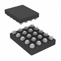
YFP PACKAGE
(TOP VIEW)
1 2 3 4
A
B
C
D
E
TERMINAL ASSIGNMENTS
1
2
3
4
A
DAT2A
VCCA
WP
DAT2B
B
DAT3A
CD
VCCB
DAT3B
C
CMDA
GND
GND
CMDB
D
DAT0A
CLKA
CLKB
DAT0B
E
DAT1A
CLK-f
EN
DAT1B
DESCRIPTION/ORDERING INFORMATION
The TXS0206 is a level shifter for interfacing microprocessors with MultiMediaCards (MMCs), secure digital (SD)
cards, and Memory Stick™ cards. It includes a high-speed level translator along with ESD protection and EMI
filtering circuitry.
The voltage-level translator has two supply voltage pins. VCCA as well as VCCB can be operated over the full
range of 1.1 V to 3.6 V. The TXS0206 enables system designers to easily interface applications processors or
digital basebands to memory cards and SDIO peripherals operating at a different I/O voltage level.
Memory card standards recommend high-ESD protection for devices that connect directly to the external memory
card. To meet this need, the TXS0206 incorporates ±8-kV Contact Discharge protection on the card side.
The TXS0206 is offered in a 20-bump wafer chip scale package (WCSP). This package has dimensions of
1.96 mm × 1.56 mm, with a 0.4-mm ball pitch for effective board-space savings. Memory cards are widely used
in mobile phones, PDAs, digital cameras, personal media players, camcorders, set-top boxes, etc. Low static
power consumption and small package size make the TXS0206 an ideal choice for these applications.
ORDERING INFORMATION (1)
TA
–40°C to 85°C
(1)
(2)
(3)
PACKAGE (2)
WCSP – YFP (Pb-free)
Tape and reel
ORDERABLE PART NUMBER
TXS0206YFPR
TOP-SIDE MARKING (3)
_ _ _3T_
For the most current package and ordering information, see the Package Option Addendum at the end of this document, or see the TI
web site at www.ti.com.
Package drawings, thermal data, and symbolization are available at www.ti.com/packaging.
YFP: The actual top-side marking has three preceding characters to denote year, month, and sequence code, and one following
character to designate the assembly/test site. Pin 1 identifier indicates solder-bump composition (1 = SnPb, •= Pb-free).
1
2
Please be aware that an important notice concerning availability, standard warranty, and use in critical applications of Texas
Instruments semiconductor products and disclaimers thereto appears at the end of this data sheet.
All trademarks are the property of their respective owners.
PRODUCTION DATA information is current as of publication date.
Products conform to specifications per the terms of the Texas
Instruments standard warranty. Production processing does not
necessarily include testing of all parameters.
Copyright © 2009–2010, Texas Instruments Incorporated
�TXS0206
SCES697C – AUGUST 2009 – REVISED JANUARY 2010
www.ti.com
REFERENCE DESIGN
VCCA
VCCB
C3
0.1 µF
U1A
VCCB
C4
0.1 µF
C1
0.1 µF
J1
U2
VDDA
DAT0
DAT1
DAT2
DAT3
CMD
CLK
CLKin
GND
WP
A2
D1
E1
A1
B1
C1
D2
E2
C2
C3
VCCA
VCCB
DAT0A
DAT1A
DAT2A
DAT3A
CMDA
CLKA
CLK-f
B3
D4 DAT0B
DAT0B
DAT1B E4 DAT1B
DAT2B A4 DAT2B
DAT3B B4 DAT3B
C4 CMDB
CMDB
D3 CLKB
CLKB
GND
A3 WP
WP
B2 CD
CD
GND
CD
Processor
SD/SDIO MMC
DAT2B
DAT3B
CMDB
CLKB
DAT0B
DAT1B
CD
WP
0
1
2
3
4
5
6
7
8
9
10
11
12
13
DAT2
DAT3
CMD
VSS1
VDD
CLK
VSS2
DAT0
DAT1
WP/CD (Physical)
CD (Physical)
GND
GND
WP (Physical)
54794-0978
SD/SDIO Card
Connector
TXS0206
Figure 1. Interfacing With SD/SDIO Card
2
Submit Documentation Feedback
Copyright © 2009–2010, Texas Instruments Incorporated
Product Folder Link(s): TXS0206
�TXS0206
www.ti.com
SCES697C – AUGUST 2009 – REVISED JANUARY 2010
VCCA
VCCB
C3
0.1 µF
U1A
VCCB
C4
0.1 µF
C1
0.1 µF
U2
VDDA
DAT0
DAT1
DAT2
DAT3
CMD
CLK
CLKin
GND
A2
D1
E1
A1
B1
C1
D2
E2
C2
C3
VCCA
VCCB
DAT0A
CMDB
2
DAT1B
3
E4 DAT1B
DAT1B
A4 DAT2B
DAT2B
B4 DAT3B
DAT3B
DAT0B
4
DAT2B
5
CD
6
C4 CMDB
CMDB
D3 CLKB
CLKB
DAT3B
7
CLKB
8
DAT0B
DAT3A
CMDA
CLKA
CLK-f
GND
9
GND
CD
CD
Memory Stick™
Controller
D4 DAT0B
DAT1A
DAT2A
1
B3
B2 CD
10
TXS0206
VSS
BS
DATA1 (see Note)
DATA0/SDIO (see Note)
DATA2 (see Note)
INS
DATA3 (see Note)
SCLK
VCC
VSS
Memory Stick™
Connector
NOTE: The TXS0206 has integrated pullup resistor values that dynamically change value depending on whether a low or
high signal is being transmitted through the device. When the output is low, the TXS0206 internal pullup value is
40 kΩ, and when the output is high, the internal pullup value change to a value of 4 kΩ. For MSA and MSH Memory
Stick™ memory cards, to ensure that a valid VIH (i.e., receiver input voltage high) is achieved, the internal pulldown
resistors for these memory cards are not smaller than a 10-kΩ value. See the Application Information section of this
data sheet, which explains the impact of adding too heavy (i.e.,
很抱歉,暂时无法提供与“TXS0206YFPR”相匹配的价格&库存,您可以联系我们找货
免费人工找货