Product
Folder
Sample &
Buy
Technical
Documents
Support &
Community
Tools &
Software
UA78L02A, UA78L05, UA78L05A, UA78L06A
UA78L08A, UA78L09A, UA78L10A, UA78L12A, UA78L15A
SLVS010V – JANUARY 1976 – REVISED NOVEMBER 2016
UA78L00 Series Positive-Voltage Linear Regulators
1 Features
3 Description
•
•
•
•
•
The UA78L00 series of fixed-voltage linear regulators
is designed for a wide range of applications. These
applications include on-card regulation for elimination
of noise and distribution problems associated with
single-point regulation as well as for voltage
regulation in major appliances. In addition, they can
be used with power-pass elements to make highcurrent voltage regulators. One of these regulators
can deliver up to 100 mA of output current. The
internal limiting and thermal-shutdown features of
these regulators help to protect the device from
overload.
1
3-Terminal Linear Regulators
Output Current Up to 100 mA
No External Components
Internal Thermal-Overload Protection
Internal Short-Circuit Current Limiting
2 Applications
•
•
•
•
•
•
•
Computing and Servers
On-Card Regulation
Telecommunications
White Goods
Chemical or Gas Sensors
Field Transmitter: Temperature Sensors
Flow Meters
The UA78L00C and UA78L00AC series devices are
characterized for operation over the virtual junction
temperature range of 0°C to 125°C. The UA78L05AI
device is characterized for operation over the virtual
junction temperature range of −40°C to 125°C.
Device Information(1)
PART NUMBER
PACKAGE
BODY SIZE (NOM)
UA78L00D,
UA78L00AD
SOIC (8)
4.90 mm × 3.91 mm
UA78L00LP,
UA78L00ALP
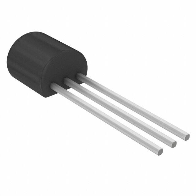
TO-92 (3)
4.30 mm × 4.30 mm
UA78L00PK,
UA78L00APK
SOT-89 (3)
4.50 mm × 2.50 mm
(1) For all available packages, see the orderable addendum at
the end of the data sheet.
Simplified Schematic
UA78L00
VI
0.33 F
INPUT
OUTPUT
COMMON
VO
0.1 F
Copyright © 2016, Texas Instruments Incorporated
1
An IMPORTANT NOTICE at the end of this data sheet addresses availability, warranty, changes, use in safety-critical applications,
intellectual property matters and other important disclaimers. PRODUCTION DATA.
�UA78L02A, UA78L05, UA78L05A, UA78L06A
UA78L08A, UA78L09A, UA78L10A, UA78L12A, UA78L15A
SLVS010V – JANUARY 1976 – REVISED NOVEMBER 2016
www.ti.com
Table of Contents
1
2
3
4
5
6
7
Features ..................................................................
Applications ...........................................................
Description .............................................................
Revision History.....................................................
Pin Configuration and Functions .........................
Specifications.........................................................
1
1
1
2
3
4
6.1
6.2
6.3
6.4
6.5
6.6
6.7
6.8
6.9
6.10
6.11
6.12
6.13
4
4
4
4
5
5
6
6
7
7
8
8
9
Absolute Maximum Ratings ......................................
ESD Ratings..............................................................
Recommended Operating Conditions.......................
Thermal Information ..................................................
Electrical Characteristics: UA78L02..........................
Electrical Characteristics: UA78L05..........................
Electrical Characteristics: UA78L06..........................
Electrical Characteristics: UA78L08..........................
Electrical Characteristics: UA78L09..........................
Electrical Characteristics: UA78L10........................
Electrical Characteristics: UA78L12........................
Electrical Characteristics: UA78L15........................
Typical Characteristics ............................................
Detailed Description ............................................ 10
7.1
7.2
7.3
7.4
8
Overview .................................................................
Functional Block Diagram .......................................
Feature Description.................................................
Device Functional Modes........................................
10
10
10
10
Applications and Implementation ...................... 11
8.1 Application Information............................................ 11
8.2 Typical Application ................................................. 11
8.3 System Examples ................................................... 12
9 Power Supply Recommendations...................... 13
10 Layout................................................................... 13
10.1 Layout Guidelines ................................................. 13
10.2 Layout Example .................................................... 13
11 Device and Documentation Support ................. 14
11.1
11.2
11.3
11.4
11.5
11.6
Related Links ........................................................
Receiving Notification of Documentation Updates
Community Resource............................................
Trademarks ...........................................................
Electrostatic Discharge Caution ............................
Glossary ................................................................
14
14
14
14
14
14
12 Mechanical, Packaging, and Orderable
Information ........................................................... 14
4 Revision History
NOTE: Page numbers for previous revisions may differ from page numbers in the current version.
Changes from Revision U (January 2014) to Revision V
Page
•
Added Device Information table, ESD Ratings table, Feature Description section, Device Functional Modes,
Application and Implementation section, Power Supply Recommendations section, Layout section, Device and
Documentation Support section, and Mechanical, Packaging, and Orderable Information section....................................... 1
•
Added Applications ................................................................................................................................................................. 1
•
Changed θJA values in Thermal Information table From: 97 To: 115 (D), From: 140 To: 143.6 (LP), and From: 52 To:
54.7 (PK)................................................................................................................................................................................. 4
•
Changed θJC values in Thermal Information table From: 39 To: 60.3 (D), From: 55 To: 74.4 (LP), and From: 9 To:
88.1 (PK)................................................................................................................................................................................. 4
Changes from Revision T (May 2011) to Revision U
Page
•
Deleted Ordering Information table; see Product Option Addendum at the end of the data sheet........................................ 1
•
Updated document to new TI data sheet format - no specification changes ......................................................................... 1
2
Submit Documentation Feedback
Copyright © 1976–2016, Texas Instruments Incorporated
Product Folder Links: UA78L02A UA78L05 UA78L05A UA78L06A UA78L08A UA78L09A UA78L10A UA78L12A
UA78L15A
�UA78L02A, UA78L05, UA78L05A, UA78L06A
UA78L08A, UA78L09A, UA78L10A, UA78L12A, UA78L15A
www.ti.com
SLVS010V – JANUARY 1976 – REVISED NOVEMBER 2016
5 Pin Configuration and Functions
D Package
8-Pin SOIC
Top View
LP Package
3-Pin TO-92
Top View
OUTPUT
1
8
INPUT
COMMON
2
7
COMMON
COMMON
3
6
COMMON
NC
4
5
NC
INPUT
COMMON
OUTPUT
Not to scale
PK Package
3-Pin SOT-89
Top View
INPUT
COMMON
OUTPUT
Pin Functions
PIN
NAME
COMMON
SOIC
TO-92
SOT-89
I/O
DESCRIPTION
2, 3, 6, 7
2
2
—
INPUT
8
3
3
I
Supply input
OUTPUT
1
1
1
O
Voltage output
4, 5
—
—
—
No internal connection
NC
Copyright © 1976–2016, Texas Instruments Incorporated
Ground
Submit Documentation Feedback
Product Folder Links: UA78L02A UA78L05 UA78L05A UA78L06A UA78L08A UA78L09A UA78L10A UA78L12A
UA78L15A
3
�UA78L02A, UA78L05, UA78L05A, UA78L06A
UA78L08A, UA78L09A, UA78L10A, UA78L12A, UA78L15A
SLVS010V – JANUARY 1976 – REVISED NOVEMBER 2016
www.ti.com
6 Specifications
6.1 Absolute Maximum Ratings
over operating free-air temperature range (unless otherwise noted) (1)
MIN
Input voltage, VI
MAX
UA78L02AC, UA78L05C, UA78L09C, and UA78L10AC
30
UA78L12C, UA78L12AC, UA78L15C, and UA78L15AC
35
Virtual junction temperature, TJ
Storage temperature, Tstg
(1)
–65
UNIT
V
150
°C
150
°C
Stresses beyond those listed under Absolute Maximum Ratings may cause permanent damage to the device. These are stress ratings
only, and functional operation of the device at these or any other conditions beyond those indicated under Recommended Operating
Conditions is not implied. Exposure to absolute-maximum-rated conditions for extended periods may affect device reliability.
6.2 ESD Ratings
VALUE
V(ESD)
(1)
(2)
Electrostatic discharge
Human body model (HBM), per ANSI/ESDA/JEDEC JS-001, all pins (1)
1000
Charged device model (CDM), per JEDEC specification JESD22-C101, all
pins (2)
1000
UNIT
V
JEDEC document JEP155 states that 500-V HBM allows safe manufacturing with a standard ESD control process.
JEDEC document JEP157 states that 250-V CDM allows safe manufacturing with a standard ESD control process.
6.3 Recommended Operating Conditions
UA78L02AC
VI
Input voltage
IO
MIN
MAX
4.75
20
UA78L05C and UA78L05AC
7
20
UA78L06C and UA78L06AC
8.5
20
UA78L08C and UA78L08AC
10.5
23
UA78L09C and UA78L09AC
11.5
24
UA78L10AC
12.5
25
UA78L12C and UA78L12AC
14.5
27
UA78L15C and UA78L15AC
17.5
TJ
100
Operating virtual junction temperature
UA78L05AI
V
30
Output current
UA78L00C and UA78L00AC series
UNIT
0
125
–40
125
mA
°C
6.4 Thermal Information
UA78L00
THERMAL METRIC (1)
D (SOIC)
LP (TO-92)
PK (SOT-89)
8 PINS
3 PINS
3 PINS
UNIT
RθJA
Junction-to-ambient thermal resistance
115
143.6
54.7
°C/W
RθJC(top)
Junction-to-case (top) thermal resistance
60.3
74.4
88.1
°C/W
RθJB
Junction-to-board thermal resistance
55.6
—
9.6
°C/W
ψJT
Junction-to-top characterization parameter
16.2
24.2
6.2
°C/W
ψJB
Junction-to-board characterization parameter
55
120.9
9.7
°C/W
RθJC(bot)
Junction-to-case (bottom) thermal resistance
—
—
7.7
°C/W
(1)
4
For more information about traditional and new thermal metrics, see the Semiconductor and IC Package Thermal Metrics application
report.
Submit Documentation Feedback
Copyright © 1976–2016, Texas Instruments Incorporated
Product Folder Links: UA78L02A UA78L05 UA78L05A UA78L06A UA78L08A UA78L09A UA78L10A UA78L12A
UA78L15A
�UA78L02A, UA78L05, UA78L05A, UA78L06A
UA78L08A, UA78L09A, UA78L10A, UA78L12A, UA78L15A
www.ti.com
SLVS010V – JANUARY 1976 – REVISED NOVEMBER 2016
6.5 Electrical Characteristics: UA78L02
at specified virtual junction temperature, VI = 9 V, and IO = 40 mA (unless otherwise noted) (1)
TEST CONDITIONS (2)
PARAMETER
VI = 4.75 V to 20 V, and IO = 1 mA to 40 mA
Output voltagef
TJ = 25°C
TJ = 0°C to 125°C
IO = 1 mA to 70 mA, and TJ = 0°C to 125°C
Input voltage regulation
Ripple rejection
TYP
2.5
2.6
MAX
2.75
2.45
2.75
20
100
VI = 5 V to 20 V, and TJ = 25°C
16
75
43
UNIT
2.7
2.45
VI = 4.75 V to 20 V, and TJ = 25°C
VI = 6 V to 20 V, f = 120 Hz, and TJ = 25°C
Output voltage regulation
MIN
V
mV
51
dB
IO = 1 mA to 100 mA, and TJ = 25°C
12
50
IO = 1 mA to 40 mA, and TJ = 25°C
6
25
mV
Output noise voltage
f = 10 Hz to 100 kHz, and TJ = 25°C
30
µV
Dropout voltage
TJ = 25°C
1.7
V
TJ = 25°C
3.6
Bias current
Bias current change
(1)
(2)
6
TJ = 125°C
5.5
VI = 5 V to 20 V, and TJ = 0°C to 125°C
2.5
IO = 1 mA to 40 mA, and TJ = 0°C to 125°C
0.1
mA
mA
Applies to UA78L02AC.
Pulse-testing techniques maintain TJ as close to TA as possible. Thermal effects must be taken into account separately. All
characteristics are measured with a 0.33-µF capacitor across the input and a 0.1-µF capacitor across the output.
6.6 Electrical Characteristics: UA78L05
at specified virtual junction temperature, VI = 10 V, and IO = 40 mA (unless otherwise noted)
TEST CONDITIONS (1)
PARAMETER
TJ = 25°C
VI = 7 V to 20 V, and
IO = 1 mA to 40 mA
Output voltage
Input voltage
regulation
Ripple rejection
Output voltage
regulation
TJ = full range
MIN
TYP
MAX
UA78L05C
4.6
5
5.4
UA78L05AC and
UA78L05AI
4.8
5
5.2
UA78L05C
4.5
5.5
4.75
5.25
UA78L05AC and
UA78L05AI
IO = 1 mA to 70 mA, and
TJ = full range
UA78L05C
VI = 7 V to 20 V, and
TJ = 25°C
UA78L05C
32
200
UA78L05AC and UA78L05AI
32
150
VI = 8 V to 20 V, and
TJ = 25°C
UA78L05C
26
150
UA78L05AC and UA78L05AI
26
100
VI = 8 V to 18 V, f = 120 Hz,
and TJ = 25°C
UA78L05C
40
49
UA78L05AC and UA78L05AI
41
49
UA78L05AC and UA78L05AI
4.5
5.5
4.75
5.25
15
60
IO = 1 mA to 40 mA, and TJ = 25°C
8
30
42
Dropout voltage
TJ = 25°C
1.7
TJ = 25°C
3.8
Bias current
TJ = 125°C
(1)
IO = 1 mA to 40 mA, and
TJ = full range
mV
mV
μV
V
6
5.5
VI = 8 V to 20 V, and TJ = full range
Bias current change
V
dB
IO = 1 mA to 100 mA, and TJ = 25°C
Output noise voltage f = 10 Hz to 100 kHz, and TJ = 25°C
UNIT
mA
1.5
UA78L05C
0.2
UA78L05AC and UA78L05AI
0.1
mA
Pulse-testing techniques maintain TJ as close to TA as possible. Thermal effects must be taken into account separately. All
characteristics are measured with a 0.33-μF capacitor across the input and a 0.1-μF capacitor across the output. Full range for the
UA78L05AC is TJ = 0°C to 125°C, and full range for the UA78L05AI is TJ = –40°C to 125°C.
Copyright © 1976–2016, Texas Instruments Incorporated
Submit Documentation Feedback
Product Folder Links: UA78L02A UA78L05 UA78L05A UA78L06A UA78L08A UA78L09A UA78L10A UA78L12A
UA78L15A
5
�UA78L02A, UA78L05, UA78L05A, UA78L06A
UA78L08A, UA78L09A, UA78L10A, UA78L12A, UA78L15A
SLVS010V – JANUARY 1976 – REVISED NOVEMBER 2016
www.ti.com
6.7 Electrical Characteristics: UA78L06
at specified virtual junction temperature, VI = 12 V, and IO = 40 mA (unless otherwise noted)
TEST CONDITIONS (1)
PARAMETER
TJ = 25°C
VI = 8.5 V to 20 V,
IO = 1 mA to 40 mA
Output voltage
TJ = 0°C to 125°C
TJ = 0°C to 125°C, and IO = 1 mA to 70 mA
VI = 8.5 V to 20 V
Input voltage
regulation
TJ = 25°C
VI = 9 V to 20 V
Ripple rejection
TJ = 25°C, VI = 10 V to 20 V, and f = 120 Hz
Output voltage
regulation
TJ = 25°C
UA78L06C
UA78L06AC
MIN
TYP
5.7
6.2
6.7
5.95
6.2
6.45
UA78L06C
5.6
6.8
UA78L06AC
5.9
6.5
UA78L06C
5.6
6.8
UA78L06AC
5.9
35
200
UA78L06AC
35
175
UA78L06C
29
150
UA78L06AC
29
125
UA78L06C
39
48
UA78L06AC
40
48
16
80
IO = 1 mA to 40 mA
9
40
46
TJ = 25°C
1.7
TJ = 25°C
3.9
VI = 9 V to 20 V
(1)
mV
V
6
5.5
IO = 1 mA to 40 mA
mV
µV
TJ = 125°C
TJ = 0°C to 125°C
V
dB
IO = 1 mA to 100 mA
Dropout voltage
Bias current change
UNIT
6.5
UA78L06C
Output noise voltage TJ = 25°C, and f = 10 Hz to 100 kHz
Bias current
MAX
mA
1.5
UA78L06C
0.2
UA78L06AC
0.1
mA
Pulse-testing techniques maintain TJ as close to TA as possible. Thermal effects must be taken into account separately. All
characteristics are measured with a 0.33-µF capacitor across the input and a 0.1-µF capacitor across the output.
6.8 Electrical Characteristics: UA78L08
at specified virtual junction temperature, VI = 14 V, and IO = 40 mA (unless otherwise noted)
TEST CONDITIONS (1)
PARAMETER
TJ = 25°C
VI = 10.5 V to 23 V,
IO = 1 mA to 40 mA
Output voltage
TJ = 0°C to 125°C
IO = 1 mA to 70 mA
TJ = 0°C to 125°C
VI = 10.5 V to 23 V
Input voltage
regulation
TJ = 25°C
VI = 11 V to 23 V
Ripple rejection
VI = 13 V to 23 V, f = 120 Hz, and TJ = 25°C
Output voltage
regulation
TJ = 25°C
MIN
TYP
MAX
7.36
8
8.64
UA78L08AC
7.7
8
8.3
UA78L08C
7.2
8.8
UA78L08AC
7.6
8.4
UA78L08C
7.2
8.8
UA78L08AC
7.6
8.4
UA78L08C
UA78L08C
42
200
UA78L08AC
42
175
UA78L08C
36
150
36
125
UA78L08AC
UA78L08C
36
46
UA78L08AC
37
46
UNIT
V
mV
dB
IO = 1 mA to 100 mA
18
80
IO = 1 mA to 40 mA
10
40
mV
Output noise voltage f = 10 Hz to 100 kHz, and TJ = 25°C
54
µV
Dropout voltage
TJ = 25°C
1.7
V
TJ = 25°C
4
Bias current
(1)
6
TJ = 125°C
6
5.5
mA
Pulse-testing techniques maintain TJ as close to TA as possible. Thermal effects must be taken into account separately. All
characteristics are measured with a 0.33-µF capacitor across the input and a 0.1-µF capacitor across the output.
Submit Documentation Feedback
Copyright © 1976–2016, Texas Instruments Incorporated
Product Folder Links: UA78L02A UA78L05 UA78L05A UA78L06A UA78L08A UA78L09A UA78L10A UA78L12A
UA78L15A
�UA78L02A, UA78L05, UA78L05A, UA78L06A
UA78L08A, UA78L09A, UA78L10A, UA78L12A, UA78L15A
www.ti.com
SLVS010V – JANUARY 1976 – REVISED NOVEMBER 2016
Electrical Characteristics: UA78L08 (continued)
at specified virtual junction temperature, VI = 14 V, and IO = 40 mA (unless otherwise noted)
TEST CONDITIONS (1)
PARAMETER
MIN
TYP
MAX
VI = 11 V to 23 V
Bias current change
TJ = 0°C to 125°C
IO = 1 mA to 40 mA
UNIT
1.5
UA78L08C
0.2
UA78L08AC
0.1
mA
6.9 Electrical Characteristics: UA78L09
at specified virtual junction temperature, VI = 16 V, and IO = 40 mA (unless otherwise noted)
TEST CONDITIONS (1)
PARAMETER
TJ = 25°C
VI = 12 V to 24 V,
IO = 1 mA to 40 mA
Output voltage
TJ = 0°C to 125°C
IO = 1 mA to 70 mA, and TJ = 0°C to 125°C
VI = 12 V to 24 V
Input voltage
regulation
TJ = 25°C
VI = 13 V to 24 V
Ripple rejection
VI = 15 V to 25 V, f = 120 Hz, and TJ = 25°C
Output voltage
regulation
TJ = 25°C
MIN
TYP
MAX
UA78L09C
8.3
9
9.7
UA78L09AC
8.6
9
9.4
UA78L09C
UA78L09AC
UA78L09C
UA78L09AC
8.1
9.9
8.55
9.45
8.1
9.9
8.55
45
225
UA78L09AC
45
175
UA78L09C
40
175
40
125
UA78L09C
36
45
UA78L09AC
38
45
19
90
IO = 1 mA to 40 mA
11
40
58
Dropout voltage
TJ = 25°C
1.7
TJ = 25°C
4.1
V
6
TJ = 125°C
(1)
TJ = 0°C to 125°C
5.5
IO = 1 mA to 40 mA
mV
µV
VI = 13 V to 24 V
Bias current change
mV
dB
IO = 1 mA to 100 mA
Output noise voltage f = 10 Hz to 100 kHz, and TJ = 25°C
Bias current
V
9.45
UA78L09C
UA78L09AC
UNIT
mA
1.5
UA78L09C
0.2
UA78L09AC
0.1
mA
Pulse-testing techniques maintain TJ as close to TA as possible. Thermal effects must be taken into account separately. All
characteristics are measured with a 0.33-µF capacitor across the input and a 0.1-µF capacitor across the output.
6.10 Electrical Characteristics: UA78L10
at specified virtual junction temperature, VI = 14 V, and IO = 40 mA (unless otherwise noted) (1)
TEST CONDITIONS (2)
PARAMETER
Output voltage
VI = 13 V to 25 V, and IO =
1 mA to 40 mA
MIN
TYP
MAX
TJ = 25°C
9.6
10
10.4
TJ = 0°C to 125°C
9.5
10.5
9.5
10.5
TJ = 0°C to 125°C, and IO = 1 mA to 70 mA
VI = 13 V to 25 V
51
175
VI = 14 V to 25 V
42
125
Input voltage regulation
TJ = 25°C
Ripple rejection
TJ = 25°C, VI = 15 V to 25 V, and f = 120 Hz
37
44
UNIT
V
mV
dB
IO = 1 mA to 100 mA
20
90
IO = 1 mA to 40 mA
11
40
Output voltage regulation
TJ = 25°C
Output noise voltage
TJ = 25°C, and f = 10 Hz to 100 kHz
62
µV
Dropout voltage
TJ = 25°C
1.7
V
(1)
(2)
mV
Applies to UA78L10AC.
Pulse-testing techniques maintain TJ as close to TA as possible. Thermal effects must be taken into account separately. All
characteristics are measured with a 0.33-µF capacitor across the input and a 0.1-µF capacitor across the output.
Copyright © 1976–2016, Texas Instruments Incorporated
Submit Documentation Feedback
Product Folder Links: UA78L02A UA78L05 UA78L05A UA78L06A UA78L08A UA78L09A UA78L10A UA78L12A
UA78L15A
7
�UA78L02A, UA78L05, UA78L05A, UA78L06A
UA78L08A, UA78L09A, UA78L10A, UA78L12A, UA78L15A
SLVS010V – JANUARY 1976 – REVISED NOVEMBER 2016
www.ti.com
Electrical Characteristics: UA78L10 (continued)
at specified virtual junction temperature, VI = 14 V, and IO = 40 mA (unless otherwise noted)(1)
TEST CONDITIONS (2)
PARAMETER
Bias current
Bias current change
MIN
TJ = 25°C
TYP
MAX
4.2
6
TJ = 125°C
TJ = 0°C to 125°C
UNIT
mA
5.5
VI = 14 V to 25 V
1.5
IO = 1 mA to 40 mA
0.1
mA
6.11 Electrical Characteristics: UA78L12
at specified virtual junction temperature, VI = 19 V, and IO = 40 mA (unless otherwise noted)
TEST CONDITIONS (1)
PARAMETER
TJ = 25°C
VI = 14 V to 27 V, and
IO = 1 mA to 40 mA
Output voltage
TJ = 0°C to 125°C
TJ = 0°C to 125°C, and IO = 1 mA to 70 mA
MIN
TYP
MAX
UA78L12C
11.1
12
12.9
UA78L12AC
11.5
12
12.5
UA78L12C
10.8
13.2
UA78L12AC
11.4
12.6
UA78L12C
10.8
13.2
UA78L12AC
11.4
UNIT
V
12.6
VI = 14.5 V to 27 V
55
250
VI = 16 V to 27 V
49
200
Input voltage regulation
TJ = 25°C
Ripple rejection
TJ = 25°C
Output voltage regulation
TJ = 25°C
Output noise voltage
TJ = 25°C, and f = 10 Hz to 100 kHz
70
µV
Dropout voltage
TJ = 25°C
1.7
V
TJ = 25°C
4.3
Bias current
VI = 15 V to 25 V, and f UA78L12C
= 120 Hz
UA78L12AC
36
42
37
42
dB
IO = 1 mA to 100 mA
22
100
IO = 1 mA to 40 mA
13
50
6.5
TJ = 125°C
6
VI = 16 V to 27 V
Bias current change
(1)
TJ = 0°C to 125°C
IO = 1 mA to 40 mA
mV
mV
mA
1.5
UA78L12C
0.2
UA78L12AC
0.1
mA
Pulse-testing techniques maintain TJ as close to TA as possible. Thermal effects must be taken into account separately. All
characteristics are measured with a 0.33-µF capacitor across the input and a 0.1-µF capacitor across the output.
6.12 Electrical Characteristics: UA78L15
at specified virtual junction temperature, VI = 23 V, and IO = 40 mA (unless otherwise noted)
TEST CONDITIONS (1)
PARAMETER
Output voltage
VI = 17.5 V to 30 V,
and IO = 1 mA to 40
mA
TJ = 25°C
TJ = 0°C to 125°C
TJ = 0°C to 125°C, and IO = 1 mA to 70 mA
Input voltage regulation
TJ = 25°C
Ripple rejection
TJ = 25°C
(1)
8
MIN
TYP
MAX
UA78L15C
13.8
15
16.2
UA78L15AC
14.4
15
15.6
UA78L15C
UA78L15AC
UA78L15C
UA78L15AC
13.5
16.5
14.25
15.75
13.5
16.5
14.25
V
15.75
VI = 17.5 V to 30 V
65
300
VI = 20 V to 30 V
58
250
VI = 18.5 V to 28.5 V,
and f = 120 Hz
UNIT
UA78L15C
33
39
UA78L15AC
34
39
mV
dB
Pulse-testing techniques maintain TJ as close to TA as possible. Thermal effects must be taken into account separately. All
characteristics are measured with a 0.33-µF capacitor across the input and a 0.1-µF capacitor across the output.
Submit Documentation Feedback
Copyright © 1976–2016, Texas Instruments Incorporated
Product Folder Links: UA78L02A UA78L05 UA78L05A UA78L06A UA78L08A UA78L09A UA78L10A UA78L12A
UA78L15A
�UA78L02A, UA78L05, UA78L05A, UA78L06A
UA78L08A, UA78L09A, UA78L10A, UA78L12A, UA78L15A
www.ti.com
SLVS010V – JANUARY 1976 – REVISED NOVEMBER 2016
Electrical Characteristics: UA78L15 (continued)
at specified virtual junction temperature, VI = 23 V, and IO = 40 mA (unless otherwise noted)
TEST CONDITIONS (1)
PARAMETER
MIN
TYP
MAX
IO = 1 mA to 100 mA
25
150
IO = 1 mA to 40 mA
15
75
Output voltage regulation
TJ = 25°C
Output noise voltage
TJ = 25°C, and f = 10 Hz to 100 kHz
82
Dropout voltage
TJ = 25°C
1.7
TJ = 25°C
4.6
Bias current
V
6.5
6
VI = 10 V to 30 V
TJ = 0°C to 125°C
mV
μV
TJ = 125°C
Bias current change
UNIT
mA
1.5
IO = 1 mA to 40 mA
UA78L15C
0.2
UA78L15AC
0.1
mA
6.13 Typical Characteristics
4.174
5.25
TA = 25qC
VI = 10 V
TA = 25qC
IO = 40 mA
5
4.17
Bias Current [mA]
Bias Current [mA]
4.172
4.168
4.166
4.164
4.75
4.5
4.25
4
4.162
4.16
3.75
0
10
20
30
40
50
60
70
Load Current (IO) [mA]
80
90
100
8
Figure 1. Bias Current vs Load Current
12
14
16
Input Voltage (VI) [V]
18
20
D002
Figure 2. Bias Current vs Input Voltage
5.1
5.1
TA = 25qC
IO = 40 mA
5.08
TA = 25qC
VI = 10 V
5.08
5.06
5.06
Output Voltage (VO) [V]
Output Voltage (VO) [V]
10
D001
5.04
5.02
5
4.98
4.96
5.04
5.02
5
4.98
4.96
4.94
4.94
4.92
4.92
4.9
4.9
6
8
10
12
14
16
Input Voltage (VI) [V]
Figure 3. Line Regulation
Copyright © 1976–2016, Texas Instruments Incorporated
18
20
D003
0
10
20
30
40
50
60
70
Output Current (IO) [mA]
80
90
100
D004
Figure 4. Load Regulation
Submit Documentation Feedback
Product Folder Links: UA78L02A UA78L05 UA78L05A UA78L06A UA78L08A UA78L09A UA78L10A UA78L12A
UA78L15A
9
�UA78L02A, UA78L05, UA78L05A, UA78L06A
UA78L08A, UA78L09A, UA78L10A, UA78L12A, UA78L15A
SLVS010V – JANUARY 1976 – REVISED NOVEMBER 2016
www.ti.com
7 Detailed Description
7.1 Overview
The UA78L00 series of fixed-voltage integrated-circuit voltage regulators is designed for a wide range of
applications. Each of these regulators can deliver up to 100 mA of output current at a fixed output voltage
depending on the device variant.
7.2 Functional Block Diagram
INPUT
20 kW
OUTPUT
1 kW to 14 kW
1.4 kW
COMMON
Copyright © 2016, Texas Instruments Incorporated
NOTE: Resistor values shown are nominal.
7.3 Feature Description
The UA78L00 series of linear regulators are easy-to-use, fixed-output voltage regulators. The devices enable up
to 100 mA of current and feature short-circuit current limiting and thermal overload protection.
7.4 Device Functional Modes
7.4.1 Fixed-Output Mode
These devices are available in fixed-output voltages. Table 1 describes the typical output voltage provided by
each device variation.
Table 1. UA78L00 Typical Device Voltage Outputs
10
Submit Documentation Feedback
DEVICE
TYPICAL OUTPUT VOLTAGE (V)
UA78L02
2.6
UA78L05
5
UA78L06
6.2
UA78L08
8
UA78L09
9
UA78L10
10
UA78L12
12
UA78L15
15
Copyright © 1976–2016, Texas Instruments Incorporated
Product Folder Links: UA78L02A UA78L05 UA78L05A UA78L06A UA78L08A UA78L09A UA78L10A UA78L12A
UA78L15A
�UA78L02A, UA78L05, UA78L05A, UA78L06A
UA78L08A, UA78L09A, UA78L10A, UA78L12A, UA78L15A
www.ti.com
SLVS010V – JANUARY 1976 – REVISED NOVEMBER 2016
8 Applications and Implementation
NOTE
Information in the following applications sections is not part of the TI component
specification, and TI does not warrant its accuracy or completeness. TI’s customers are
responsible for determining suitability of components for their purposes. Customers should
validate and test their design implementation to confirm system functionality.
8.1 Application Information
The UA78L00 devices are ideal for use as linear regulators with only a few external components needed. The
UA78L00 devices can also be used to clean power supply noise by attenuating ripple on the input signal.
8.2 Typical Application
The UA78L00 devices are typically used as fixed-output linear regulators, sourcing current up to 100 mA into a
load.
UA78L00
VI
INPUT
OUTPUT
COMMON
0.33 F
VO
0.1 F
Copyright © 2016, Texas Instruments Incorporated
Figure 5. Fixed Output Regulator
8.2.1 Design Requirements
The COMMON pin must be tied to ground to set the OUTPUT pin to the desired fixed output voltage.
Although not required, a 0.33-µF bypass capacitor is recommended on the input, and a 0.1-µF bypass capacitor
is recommend on the output.
8.2.2 Detailed Design Procedure
Occasionally, the input voltage to the regulator can collapse faster than the output voltage. For example, this can
occur when the input supply is crowbarred during an output overvoltage condition. If the output voltage is greater
than approximately 7 V, the emitter-base junction of the series-pass element (internal or external) could break
down and be damaged. To prevent this, a diode shunt can be employed as shown in Figure 6.
1N4001 or
Equivalent
UA78L00
VI
INPUT
0.33 F
OUTPUT
COMMON
VO
0.1 F
Copyright © 2016, Texas Instruments Incorporated
Figure 6. Reverse-Bias-Protection Circuit
Copyright © 1976–2016, Texas Instruments Incorporated
Submit Documentation Feedback
Product Folder Links: UA78L02A UA78L05 UA78L05A UA78L06A UA78L08A UA78L09A UA78L10A UA78L12A
UA78L15A
11
�UA78L02A, UA78L05, UA78L05A, UA78L06A
UA78L08A, UA78L09A, UA78L10A, UA78L12A, UA78L15A
SLVS010V – JANUARY 1976 – REVISED NOVEMBER 2016
www.ti.com
Typical Application (continued)
In many cases, a regulator powers a load that is not connected to ground, but instead, is connected to a voltage
source of opposite polarity (for example, operational amplifiers, level-shifting circuits, and so on). In these cases,
a clamp diode should be connected to the regulator output as shown in Figure 7. This protects the regulator from
output polarity reversals during startup and short-circuit operation.
1N4001 or
Equivalent
UA78L00
VI
INPUT
OUTPUT
COMMON
0.33 F
VO
0.1 F
-VO
Copyright © 2016, Texas Instruments Incorporated
Figure 7. Output Polarity-Reversal-Protection Circuit
8.2.3 Application Curves
7
TA = 25qC
VO = 40 mA (@ 5V)
Output Voltage (VO) [V]
6
5
4
3
2
1
0
0
2
4
6
8
10
12
14
Input Voltage (VO) [V]
16
18
20
D005
Figure 8. Output Voltage vs Input Voltage
8.3 System Examples
8.3.1 Positive Regulator in Negative Configuration
UA78L00
+
VI
-
INPUT
OUTPUT
GND
COMMON
-VO
Copyright © 2016, Texas Instruments Incorporated
Figure 9. Positive Regulator in Negative Configuration (VI Must Float)
8.3.2 Current Limiter Circuit
Figure 10 shows an example of using the UA78L00 as a current limiter. The output current limit is set by
Equation 1.
æV ö
I O = ç O ÷ + I O Bias Current
è R1 ø
(1)
12
Submit Documentation Feedback
Copyright © 1976–2016, Texas Instruments Incorporated
Product Folder Links: UA78L02A UA78L05 UA78L05A UA78L06A UA78L08A UA78L09A UA78L10A UA78L12A
UA78L15A
�UA78L02A, UA78L05, UA78L05A, UA78L06A
UA78L08A, UA78L09A, UA78L10A, UA78L12A, UA78L15A
www.ti.com
SLVS010V – JANUARY 1976 – REVISED NOVEMBER 2016
System Examples (continued)
IO
UA78L00
VI
INPUT
OUTPUT
Output
R1
COMMON
+ VO(Reg) -
Copyright © 2016, Texas Instruments Incorporated
Figure 10. Current Limiter Example
9 Power Supply Recommendations
See Recommended Operating Conditions for the recommended power supply voltages for each variation of the
UA78L00. Note that each device variant may have a different recommended maximum operating voltage.
10 Layout
10.1 Layout Guidelines
Keep trace widths large enough to eliminate problematic I×R voltage drops at the input and output terminals.
Bypass capacitors should be placed as close to the UA78L00 as possible. Additional copper and vias connected
to ground facilitate additional thermal dissipation, preventing the device from reaching thermal overload.
10.2 Layout Example
VO
0.1 F
INPUT
COMMON
OUTPUT
Ground
0.33 F
VI
Figure 11. Example Layout for PK Package
Copyright © 1976–2016, Texas Instruments Incorporated
Submit Documentation Feedback
Product Folder Links: UA78L02A UA78L05 UA78L05A UA78L06A UA78L08A UA78L09A UA78L10A UA78L12A
UA78L15A
13
�UA78L02A, UA78L05, UA78L05A, UA78L06A
UA78L08A, UA78L09A, UA78L10A, UA78L12A, UA78L15A
SLVS010V – JANUARY 1976 – REVISED NOVEMBER 2016
www.ti.com
11 Device and Documentation Support
11.1 Related Links
The table below lists quick access links. Categories include technical documents, support and community
resources, tools and software, and quick access to sample or buy.
Table 2. Related Links
PARTS
PRODUCT FOLDER
SAMPLE & BUY
TECHNICAL
DOCUMENTS
TOOLS &
SOFTWARE
SUPPORT &
COMMUNITY
UA78L02A
Click here
Click here
Click here
Click here
Click here
UA78L05
Click here
Click here
Click here
Click here
Click here
UA78L05A
Click here
Click here
Click here
Click here
Click here
UA78L06A
Click here
Click here
Click here
Click here
Click here
UA78L08A
Click here
Click here
Click here
Click here
Click here
UA78L09A
Click here
Click here
Click here
Click here
Click here
UA78L10A
Click here
Click here
Click here
Click here
Click here
UA78L12A
Click here
Click here
Click here
Click here
Click here
UA78L15A
Click here
Click here
Click here
Click here
Click here
11.2 Receiving Notification of Documentation Updates
To receive notification of documentation updates, navigate to the device product folder on ti.com. In the upper
right corner, click on Alert me to register and receive a weekly digest of any product information that has
changed. For change details, review the revision history included in any revised document.
11.3 Community Resource
The following links connect to TI community resources. Linked contents are provided "AS IS" by the respective
contributors. They do not constitute TI specifications and do not necessarily reflect TI's views; see TI's Terms of
Use.
TI E2E™ Online Community TI's Engineer-to-Engineer (E2E) Community. Created to foster collaboration
among engineers. At e2e.ti.com, you can ask questions, share knowledge, explore ideas and help
solve problems with fellow engineers.
Design Support TI's Design Support Quickly find helpful E2E forums along with design support tools and
contact information for technical support.
11.4 Trademarks
E2E is a trademark of Texas Instruments.
All other trademarks are the property of their respective owners.
11.5 Electrostatic Discharge Caution
These devices have limited built-in ESD protection. The leads should be shorted together or the device placed in conductive foam
during storage or handling to prevent electrostatic damage to the MOS gates.
11.6 Glossary
SLYZ022 — TI Glossary.
This glossary lists and explains terms, acronyms, and definitions.
12 Mechanical, Packaging, and Orderable Information
The following pages include mechanical, packaging, and orderable information. This information is the most
current data available for the designated devices. This data is subject to change without notice and revision of
this document. For browser-based versions of this data sheet, refer to the left-hand navigation.
14
Submit Documentation Feedback
Copyright © 1976–2016, Texas Instruments Incorporated
Product Folder Links: UA78L02A UA78L05 UA78L05A UA78L06A UA78L08A UA78L09A UA78L10A UA78L12A
UA78L15A
�PACKAGE OPTION ADDENDUM
www.ti.com
22-Oct-2021
PACKAGING INFORMATION
Orderable Device
Status
(1)
Package Type Package Pins Package
Drawing
Qty
Eco Plan
(2)
Lead finish/
Ball material
MSL Peak Temp
Op Temp (°C)
Device Marking
(3)
(4/5)
(6)
UA78L02ACD
ACTIVE
SOIC
D
8
75
RoHS & Green
NIPDAU
Level-1-260C-UNLIM
0 to 125
78L02A
UA78L02ACDG4
ACTIVE
SOIC
D
8
75
RoHS & Green
NIPDAU
Level-1-260C-UNLIM
0 to 125
78L02A
UA78L02ACLP
ACTIVE
TO-92
LP
3
1000
RoHS &
Non-Green
SN
N / A for Pkg Type
0 to 125
78L02AC
UA78L02ACLPE3
ACTIVE
TO-92
LP
3
1000
RoHS &
Non-Green
SN
N / A for Pkg Type
0 to 125
78L02AC
UA78L05ACD
ACTIVE
SOIC
D
8
75
RoHS & Green
NIPDAU
Level-1-260C-UNLIM
0 to 125
78L05A
UA78L05ACDE4
ACTIVE
SOIC
D
8
75
RoHS & Green
NIPDAU
Level-1-260C-UNLIM
0 to 125
78L05A
UA78L05ACDG4
ACTIVE
SOIC
D
8
75
RoHS & Green
NIPDAU
Level-1-260C-UNLIM
0 to 125
78L05A
UA78L05ACDR
ACTIVE
SOIC
D
8
2500
RoHS & Green
NIPDAU | SN
Level-1-260C-UNLIM
0 to 125
78L05A
UA78L05ACDRE4
ACTIVE
SOIC
D
8
2500
RoHS & Green
NIPDAU
Level-1-260C-UNLIM
0 to 125
78L05A
UA78L05ACDRG4
ACTIVE
SOIC
D
8
2500
RoHS & Green
NIPDAU
Level-1-260C-UNLIM
0 to 125
78L05A
UA78L05ACLP
ACTIVE
TO-92
LP
3
1000
RoHS & Green
SN
N / A for Pkg Type
0 to 125
78L05AC
UA78L05ACLPE3
ACTIVE
TO-92
LP
3
1000
RoHS & Green
SN
N / A for Pkg Type
0 to 125
78L05AC
UA78L05ACLPM
ACTIVE
TO-92
LP
3
2000
RoHS & Green
SN
N / A for Pkg Type
0 to 125
78L05AC
UA78L05ACLPME3
ACTIVE
TO-92
LP
3
2000
RoHS & Green
SN
N / A for Pkg Type
0 to 125
78L05AC
UA78L05ACLPR
ACTIVE
TO-92
LP
3
2000
RoHS & Green
SN
N / A for Pkg Type
0 to 125
78L05AC
UA78L05ACLPRE3
ACTIVE
TO-92
LP
3
2000
RoHS & Green
SN
N / A for Pkg Type
0 to 125
78L05AC
UA78L05ACPK
ACTIVE
SOT-89
PK
3
1000
RoHS & Green
SN
Level-2-260C-1 YEAR
0 to 125
F5
UA78L05ACPKE6
ACTIVE
SOT-89
PK
3
1000
RoHS &
Non-Green
SNBI
Level-1-260C-UNLIM
0 to 125
F5
UA78L05ACPKG3
ACTIVE
SOT-89
PK
3
1000
RoHS & Green
SN
Level-2-260C-1 YEAR
0 to 125
F5
Addendum-Page 1
Samples
�PACKAGE OPTION ADDENDUM
www.ti.com
22-Oct-2021
Orderable Device
Status
(1)
Package Type Package Pins Package
Drawing
Qty
Eco Plan
(2)
Lead finish/
Ball material
MSL Peak Temp
Op Temp (°C)
Device Marking
(3)
(4/5)
(6)
UA78L05AID
ACTIVE
SOIC
D
8
75
RoHS & Green
NIPDAU
Level-1-260C-UNLIM
-40 to 125
78L05AI
UA78L05AIDR
ACTIVE
SOIC
D
8
2500
RoHS & Green
NIPDAU
Level-1-260C-UNLIM
-40 to 125
78L05AI
UA78L05AIDRE4
ACTIVE
SOIC
D
8
2500
RoHS & Green
NIPDAU
Level-1-260C-UNLIM
-40 to 125
78L05AI
UA78L05AILP
ACTIVE
TO-92
LP
3
1000
RoHS & Green
SN
N / A for Pkg Type
-40 to 125
78L05AI
UA78L05AILPE3
ACTIVE
TO-92
LP
3
1000
RoHS & Green
SN
N / A for Pkg Type
-40 to 125
78L05AI
UA78L05AILPR
ACTIVE
TO-92
LP
3
2000
RoHS & Green
SN
N / A for Pkg Type
-40 to 125
78L05AI
UA78L05AILPRE3
ACTIVE
TO-92
LP
3
2000
RoHS & Green
SN
N / A for Pkg Type
-40 to 125
78L05AI
UA78L05AIPK
ACTIVE
SOT-89
PK
3
1000
RoHS & Green
SN
Level-2-260C-1 YEAR
-40 to 125
J5
UA78L05AIPKG3
ACTIVE
SOT-89
PK
3
1000
RoHS & Green
SN
Level-2-260C-1 YEAR
-40 to 125
J5
UA78L05CD
ACTIVE
SOIC
D
8
75
RoHS & Green
NIPDAU
Level-1-260C-UNLIM
0 to 125
78L05C
UA78L05CDG4
ACTIVE
SOIC
D
8
75
RoHS & Green
NIPDAU
Level-1-260C-UNLIM
0 to 125
78L05C
UA78L05CDR
ACTIVE
SOIC
D
8
2500
RoHS & Green
NIPDAU
Level-1-260C-UNLIM
0 to 125
78L05C
UA78L05CDRE4
ACTIVE
SOIC
D
8
2500
RoHS & Green
NIPDAU
Level-1-260C-UNLIM
0 to 125
78L05C
UA78L05CLP
ACTIVE
TO-92
LP
3
1000
RoHS & Green
SN
N / A for Pkg Type
0 to 125
78L05C
UA78L05CLPE3
ACTIVE
TO-92
LP
3
1000
RoHS & Green
SN
N / A for Pkg Type
0 to 125
78L05C
UA78L05CLPR
ACTIVE
TO-92
LP
3
2000
RoHS & Green
SN
N / A for Pkg Type
0 to 125
78L05C
UA78L05CPK
ACTIVE
SOT-89
PK
3
1000
RoHS & Green
SN
Level-2-260C-1 YEAR
0 to 125
B5
UA78L05CPKG3
ACTIVE
SOT-89
PK
3
1000
RoHS & Green
SN
Level-2-260C-1 YEAR
0 to 125
B5
UA78L06ACLP
ACTIVE
TO-92
LP
3
1000
RoHS & Green
SN
N / A for Pkg Type
0 to 125
78L06AC
UA78L06ACLPE3
ACTIVE
TO-92
LP
3
1000
RoHS & Green
SN
N / A for Pkg Type
0 to 125
78L06AC
UA78L06ACLPR
ACTIVE
TO-92
LP
3
2000
RoHS & Green
SN
N / A for Pkg Type
0 to 125
78L06AC
Addendum-Page 2
Samples
�PACKAGE OPTION ADDENDUM
www.ti.com
22-Oct-2021
Orderable Device
Status
(1)
Package Type Package Pins Package
Drawing
Qty
Eco Plan
(2)
Lead finish/
Ball material
MSL Peak Temp
Op Temp (°C)
Device Marking
(3)
(4/5)
(6)
UA78L06ACLPRE3
ACTIVE
TO-92
LP
3
2000
RoHS & Green
SN
N / A for Pkg Type
0 to 125
78L06AC
UA78L06ACPK
ACTIVE
SOT-89
PK
3
1000
RoHS & Green
SN
Level-2-260C-1 YEAR
0 to 125
F6
UA78L06ACPKG3
ACTIVE
SOT-89
PK
3
1000
RoHS & Green
SN
Level-2-260C-1 YEAR
0 to 125
F6
UA78L08ACD
ACTIVE
SOIC
D
8
75
RoHS & Green
NIPDAU
Level-1-260C-UNLIM
0 to 125
78L08A
UA78L08ACDR
ACTIVE
SOIC
D
8
2500
RoHS & Green
NIPDAU | SN
Level-1-260C-UNLIM
0 to 125
78L08A
UA78L08ACDRG4
ACTIVE
SOIC
D
8
2500
RoHS & Green
NIPDAU
Level-1-260C-UNLIM
0 to 125
78L08A
UA78L08ACLP
ACTIVE
TO-92
LP
3
1000
RoHS & Green
SN
N / A for Pkg Type
0 to 125
78L08AC
UA78L08ACLPE3
ACTIVE
TO-92
LP
3
1000
RoHS & Green
SN
N / A for Pkg Type
0 to 125
78L08AC
UA78L08ACLPR
ACTIVE
TO-92
LP
3
2000
RoHS & Green
SN
N / A for Pkg Type
0 to 125
78L08AC
UA78L08ACLPRE3
ACTIVE
TO-92
LP
3
2000
RoHS & Green
SN
N / A for Pkg Type
0 to 125
78L08AC
UA78L08ACPK
ACTIVE
SOT-89
PK
3
1000
RoHS & Green
SN
Level-2-260C-1 YEAR
0 to 125
F8
UA78L08ACPKG3
ACTIVE
SOT-89
PK
3
1000
RoHS & Green
SN
Level-2-260C-1 YEAR
0 to 125
F8
UA78L09ACD
ACTIVE
SOIC
D
8
75
RoHS & Green
NIPDAU
Level-1-260C-UNLIM
0 to 125
78L09A
UA78L09ACDR
ACTIVE
SOIC
D
8
2500
RoHS & Green
NIPDAU
Level-1-260C-UNLIM
0 to 125
78L09A
UA78L09ACDRE4
ACTIVE
SOIC
D
8
2500
RoHS & Green
NIPDAU
Level-1-260C-UNLIM
0 to 125
78L09A
UA78L09ACLP
ACTIVE
TO-92
LP
3
1000
RoHS & Green
SN
N / A for Pkg Type
0 to 125
78L09AC
UA78L09ACLPE3
ACTIVE
TO-92
LP
3
1000
RoHS & Green
SN
N / A for Pkg Type
0 to 125
78L09AC
UA78L09ACLPR
ACTIVE
TO-92
LP
3
2000
RoHS & Green
SN
N / A for Pkg Type
0 to 125
78L09AC
UA78L09ACLPRE3
ACTIVE
TO-92
LP
3
2000
RoHS & Green
SN
N / A for Pkg Type
0 to 125
78L09AC
UA78L09ACPK
ACTIVE
SOT-89
PK
3
1000
RoHS & Green
SN
Level-2-260C-1 YEAR
0 to 125
F9
UA78L09ACPKE6
ACTIVE
SOT-89
PK
3
1000
RoHS &
Non-Green
SNBI
Level-1-260C-UNLIM
0 to 125
F9
Addendum-Page 3
Samples
�PACKAGE OPTION ADDENDUM
www.ti.com
22-Oct-2021
Orderable Device
Status
(1)
Package Type Package Pins Package
Drawing
Qty
Eco Plan
(2)
Lead finish/
Ball material
MSL Peak Temp
Op Temp (°C)
Device Marking
(3)
(4/5)
(6)
UA78L09ACPKG3
ACTIVE
SOT-89
PK
3
1000
RoHS & Green
SN
Level-2-260C-1 YEAR
0 to 125
F9
UA78L10ACD
ACTIVE
SOIC
D
8
75
RoHS & Green
NIPDAU
Level-1-260C-UNLIM
0 to 125
78L10A
UA78L10ACDR
ACTIVE
SOIC
D
8
2500
RoHS & Green
NIPDAU
Level-1-260C-UNLIM
0 to 125
78L10A
UA78L10ACDRE4
ACTIVE
SOIC
D
8
2500
RoHS & Green
NIPDAU
Level-1-260C-UNLIM
0 to 125
78L10A
UA78L10ACLP
ACTIVE
TO-92
LP
3
1000
RoHS & Green
SN
N / A for Pkg Type
0 to 125
78L10AC
UA78L10ACLPE3
ACTIVE
TO-92
LP
3
1000
RoHS & Green
SN
N / A for Pkg Type
0 to 125
78L10AC
UA78L10ACLPR
ACTIVE
TO-92
LP
3
2000
RoHS & Green
SN
N / A for Pkg Type
0 to 125
78L10AC
UA78L10ACLPRE3
ACTIVE
TO-92
LP
3
2000
RoHS & Green
SN
N / A for Pkg Type
0 to 125
78L10AC
UA78L10ACPK
ACTIVE
SOT-89
PK
3
1000
RoHS & Green
SN
Level-2-260C-1 YEAR
0 to 125
FA
UA78L10ACPKG3
ACTIVE
SOT-89
PK
3
1000
RoHS & Green
SN
Level-2-260C-1 YEAR
0 to 125
FA
UA78L12ACD
ACTIVE
SOIC
D
8
75
RoHS & Green
NIPDAU
Level-1-260C-UNLIM
0 to 125
78L12A
UA78L12ACDG4
ACTIVE
SOIC
D
8
75
RoHS & Green
NIPDAU
Level-1-260C-UNLIM
0 to 125
78L12A
UA78L12ACDR
ACTIVE
SOIC
D
8
2500
RoHS & Green
NIPDAU | SN
Level-1-260C-UNLIM
0 to 125
78L12A
UA78L12ACDRE4
ACTIVE
SOIC
D
8
2500
RoHS & Green
NIPDAU
Level-1-260C-UNLIM
0 to 125
78L12A
UA78L12ACDRG4
ACTIVE
SOIC
D
8
2500
RoHS & Green
NIPDAU
Level-1-260C-UNLIM
0 to 125
78L12A
UA78L12ACLP
ACTIVE
TO-92
LP
3
1000
RoHS & Green
SN
N / A for Pkg Type
0 to 125
78L12AC
UA78L12ACLPE3
ACTIVE
TO-92
LP
3
1000
RoHS & Green
SN
N / A for Pkg Type
0 to 125
78L12AC
UA78L12ACLPM
ACTIVE
TO-92
LP
3
2000
RoHS & Green
SN
N / A for Pkg Type
0 to 125
78L12AC
UA78L12ACLPR
ACTIVE
TO-92
LP
3
2000
RoHS & Green
SN
N / A for Pkg Type
0 to 125
78L12AC
UA78L12ACPK
ACTIVE
SOT-89
PK
3
1000
RoHS & Green
SN
Level-2-260C-1 YEAR
0 to 125
FC
UA78L12ACPKG3
ACTIVE
SOT-89
PK
3
1000
RoHS & Green
SN
Level-2-260C-1 YEAR
0 to 125
FC
Addendum-Page 4
Samples
�PACKAGE OPTION ADDENDUM
www.ti.com
22-Oct-2021
Orderable Device
Status
(1)
Package Type Package Pins Package
Drawing
Qty
Eco Plan
(2)
Lead finish/
Ball material
MSL Peak Temp
Op Temp (°C)
Device Marking
(3)
(4/5)
(6)
UA78L15ACD
ACTIVE
SOIC
D
8
75
RoHS & Green
NIPDAU
Level-1-260C-UNLIM
0 to 125
78L15A
UA78L15ACDR
ACTIVE
SOIC
D
8
2500
RoHS & Green
NIPDAU
Level-1-260C-UNLIM
0 to 125
78L15A
UA78L15ACDRE4
ACTIVE
SOIC
D
8
2500
RoHS & Green
NIPDAU
Level-1-260C-UNLIM
0 to 125
78L15A
UA78L15ACLP
ACTIVE
TO-92
LP
3
1000
RoHS & Green
SN
N / A for Pkg Type
0 to 125
78L15AC
UA78L15ACLPE3
ACTIVE
TO-92
LP
3
1000
RoHS & Green
SN
N / A for Pkg Type
0 to 125
78L15AC
UA78L15ACLPR
ACTIVE
TO-92
LP
3
2000
RoHS & Green
SN
N / A for Pkg Type
0 to 125
78L15AC
UA78L15ACLPRE3
ACTIVE
TO-92
LP
3
2000
RoHS & Green
SN
N / A for Pkg Type
0 to 125
78L15AC
UA78L15ACPK
ACTIVE
SOT-89
PK
3
1000
RoHS & Green
SN
Level-2-260C-1 YEAR
0 to 125
FF
UA78L15ACPKG3
ACTIVE
SOT-89
PK
3
1000
RoHS & Green
SN
Level-2-260C-1 YEAR
0 to 125
FF
(1)
The marketing status values are defined as follows:
ACTIVE: Product device recommended for new designs.
LIFEBUY: TI has announced that the device will be discontinued, and a lifetime-buy period is in effect.
NRND: Not recommended for new designs. Device is in production to support existing customers, but TI does not recommend using this part in a new design.
PREVIEW: Device has been announced but is not in production. Samples may or may not be available.
OBSOLETE: TI has discontinued the production of the device.
(2)
RoHS: TI defines "RoHS" to mean semiconductor products that are compliant with the current EU RoHS requirements for all 10 RoHS substances, including the requirement that RoHS substance
do not exceed 0.1% by weight in homogeneous materials. Where designed to be soldered at high temperatures, "RoHS" products are suitable for use in specified lead-free processes. TI may
reference these types of products as "Pb-Free".
RoHS Exempt: TI defines "RoHS Exempt" to mean products that contain lead but are compliant with EU RoHS pursuant to a specific EU RoHS exemption.
Green: TI defines "Green" to mean the content of Chlorine (Cl) and Bromine (Br) based flame retardants meet JS709B low halogen requirements of


 工商网监
湘ICP备2023018690号
工商网监
湘ICP备2023018690号
