µ������ ��� ��
�� �
��
������ ����������
SLVS010S − JANUARY 1976 − REVISED FEBRUARY 2004
D
D
D
D
D
3-Terminal Regulators
Output Current Up To 100 mA
No External Components
Internal Thermal-Overload Protection
Internal Short-Circuit Current Limiting
D PACKAGE
(TOP VIEW)
OUTPUT
COMMON
COMMON
NC
1
8
2
7
3
6
4
5
INPUT
COMMON
COMMON
NC
description/ordering information
This series of fixed-voltage integrated-circuit
voltage regulators is designed for a wide range of
applications. These applications include on-card
regulation for elimination of noise and distribution
problems associated with single-point regulation.
In addition, they can be used with power-pass
elements to make high-current voltage regulators.
One of these regulators can deliver up to 100 mA
of output current. The internal limiting and
thermal-shutdown features of these regulators
essentially make them immune to overload. When
used as a replacement for a Zener diode-resistor
combination, an effective improvement in output
impedance can be obtained, together with lower
bias current.
NC − No internal connection
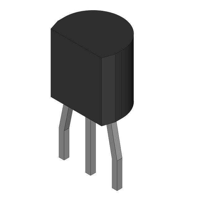
LP PACKAGE
(TO-92, TO-226AA)
(TOP VIEW)
INPUT
COMMON
OUTPUT
PK PACKAGE
(TOP VIEW)
INPUT
The µA78L00C and µA78L00AC series are
characterized for operation over the virtual
junction temperature range of 0°C to 125°C. The
µA78L05AI is characterized for operation over the
virtual junction temperature range of −40°C to
125°C.
COMMON
OUTPUT
Please be aware that an important notice concerning availability, standard warranty, and use in critical applications of
Texas Instruments semiconductor products and disclaimers thereto appears at the end of this data sheet.
Copyright 2004, Texas Instruments Incorporated
������ �� ���� ����������� �� ������� �� �� !�"#������� $���%
��$���� ������� �� �!������������ !�� �&� ����� �� ��'�� ����������
����$��$ (������)%
��$������ !��������* $��� ��� ���������#) ���#�$�
������* �� �## !���������%
POST OFFICE BOX 655303
• DALLAS, TEXAS 75265
1
�µ������ ��� ��
�� �
��
������ ����������
SLVS010S − JANUARY 1976 − REVISED FEBRUARY 2004
description/ordering information (continued)
ORDERING INFORMATION
TJ
VO(NOM)
(V)
OUTPUT
VOLTAGE
TOLERANCE
2.6 V
5%
PACKAGE†
Tube of 75
µA78L02ACD
78L02A
TO-226/TO-92 (LP)
Bulk of 1000
µA78L02ACLP
78L02AC
Tube of 75
µA78L05ACD
Reel of 2500
µA78L05ACDR
78L05A
Reel of 1000
µA78L05ACPK
F5
Bulk of 1000
µA78L05ACLP
Pack of 2000
µA78L05ACLPM
Reel of 2000
µA78L05ACLPR
Tube of 75
µA78L05CD
Reel of 2500
µA78L05CDR
78L05C
SOT-89 (PK)
Tube of
µA78L05CPK
B5
TO-92 (LP)
TO-226AA (LP)
Bulk of 1000
µA78L05CLP
Reel of 2000
µA78L05CLPR
78L05C
SOT-89 (PK)
Reel of 1000
µA78L06ACPK
F6
TO-92 (LP)
TO-226AA (LP)
Bulk of 1000
µA78L06ACLP
Reel of 2000
µA78L06ACLPR
78L06AC
Tube of 75
µA78L08ACD
78L08A
SOT-89 (PK)
5%
TO-92 (LP)
TO-226AA (LP)
5V
SOIC (D)
6.2 V
5%
SOIC (D)
5%
0°C
0
C to 125
125°C
C
8V
10%
5%
Reel of 2500
µA78L08ACDR
78L08A
Reel of 1000
µA78L08ACPK
F8
TO-92 (LP)
TO-226AA (LP)
Bulk of 1000
µA78L08ACLP
Reel of 2000
µA78L08ACLPR
Tube of 75
µA78L08CD
Reel of 2500
µA78L08CDR
Tube of 75
µA78L09ACD
Reel of 2500
µA78L09ACDR
78L09A
SOT-89 (PK)
Reel of 1000
µA78L09ACPK
F9
TO-92 (LP)
TO-226AA (LP)
Bulk of 1000
µA78L09ACLP
Reel of 2000
µA78L09ACLPR
Tube of 75
µA78L10ACD
Reel of 2500
µA78L10ACDR
78L10A
SOT-89 (PK)
Reel of 1000
µA78L10ACPK
FA
TO-92 (LP)
TO-226AA (LP)
Bulk of 1000
µA78L10ACLP
Reel of 2000
µA78L10ACLPR
Tube of 75
µA78L12ACD
Reel of 2500
µA78L12ACDR
78L12A
Reel of 1000
µA78L12ACPK
FC
Bulk of 1000
µA78L12ACLP
Pack of 2000
µA78L12ACLPM
SOIC (D)
SOIC (D)
10 V
5%
SOIC (D)
SOT-89 (PK)
12 V
78L05AC
SOT-89 (PK)
SOIC (D)
9V
TOP-SIDE
MARKING
SOIC (D)
SOIC (D)
10%
ORDERABLE
PART NUMBER
5%
TO-92 (LP)
TO-226AA (LP)
78L08AC
78L08C
78L09AC
78L10AC
78L12AC
Reel of 2000
µA78L12ACLPR
† Package drawings, standard packing quantities, thermal data, symbolization, and PCB design guidelines are available at
www.ti.com/sc/package.
2
POST OFFICE BOX 655303
• DALLAS, TEXAS 75265
�µ������ ��� ��
�� �
��
������ ����������
SLVS010S − JANUARY 1976 − REVISED FEBRUARY 2004
description/ordering information (continued)
ORDERING INFORMATION (continued)
TJ
VO(NOM)
(V)
OUTPUT
VOLTAGE
TOLERANCE
PACKAGE†
15 V
5%
µA78L15ACD
Reel of 2500
µA78L15ACDR
78L15A
SOT-89 (PK)
Reel of 1000
µA78L15ACPK
FF
TO-92 (LP)
TO-226AA (LP)
Bulk of 1000
µA78L15ACLP
Reel of 2000
µA78L15ACLPR
Tube of 75
µA78L05AID
Reel of 2500
µA78L05AIDR
78L15AI
SOT-89 (PK)
Reel of 1000
µA78L05AIPK
J5
TO-92 (LP)
TO-226AA (LP)
Bulk of 1000
µA78L05AILP
Reel of 2000
µA78L05AILPR
SOIC (D)
−40°C
−40
C to 125
125°C
C
5V
5%
TOP-SIDE
MARKING
Tube of 75
SOIC (D)
0°C
0
C to 125
125°C
C
ORDERABLE
PART NUMBER
78L15AC
78L05AI
† Package drawings, standard packing quantities, thermal data, symbolization, and PCB design guidelines are available at
www.ti.com/sc/package.
schematic
INPUT
20 kΩ
OUTPUT
1 kΩ to 14 kΩ
1.4 kΩ
COMMON
NOTE A: Resistor values shown are nominal.
POST OFFICE BOX 655303
• DALLAS, TEXAS 75265
3
�µ������ ��� ��
�� �
��
������ ����������
SLVS010S − JANUARY 1976 − REVISED FEBRUARY 2004
absolute maximum ratings over virtual junction temperature range (unless otherwise noted)†
Input voltage, VI: µA78L02AC, µA78L05C−µA78L09C, µA78L10AC . . . . . . . . . . . . . . . . . . . . . . . . . . . . . . 30 V
µA78L12C, µA78L12AC, µA78L15C, µA78L15AC . . . . . . . . . . . . . . . . . . . . . . . . . . . . . . 35 V
Virtual junction temperature, TJ . . . . . . . . . . . . . . . . . . . . . . . . . . . . . . . . . . . . . . . . . . . . . . . . . . . . . . . . . . . . 150°C
Storage temperature range, Tstg . . . . . . . . . . . . . . . . . . . . . . . . . . . . . . . . . . . . . . . . . . . . . . . . . . −65°C to 150°C
† Stresses beyond those listed under “absolute maximum ratings” may cause permanent damage to the device. These are stress ratings only, and
functional operation of the device at these or any other conditions beyond those indicated under “recommended operating conditions” is not
implied. Exposure to absolute-maximum-rated conditions for extended periods may affect device reliability.
package thermal data (see Note 1)
SOIC (D)
High K, JESD 51-7
θJC
39°C/W
TO-92/TO-226AA (LP)
High K, JESD 51-7
55°C/W
140°C/W
SOT-89 (PK)
High K, JESD 51-7
9°C/W
52°C/W
PACKAGE
BOARD
θJA
97°C/W
NOTE 1: Maximum power dissipation is a function of TJ(max), θJA, and TA. The maximum allowable power dissipation at any allowable ambient
temperature is PD = (TJ(max) − TA)/θJA. Operating at the absolute maximum TJ of 150°C can affect reliability. Due to variations in
individual device electrical characteristics and thermal resistance, the built-in thermal-overload protection may be activated at power
levels slightly above or below the rated dissipation.
recommended operating conditions
MIN
MAX
4.75
20
7
20
µA78L06C, µA78L06AC
8.5
20
µA78L08C, µA78L08AC
10.5
23
µA78L09C, µA78L09AC
11.5
24
µA78L10AC
12.5
25
µA78L12C, µA78L12AC
14.5
27
µA78L15C, µA78L15AC
17.5
µA78L02AC
µA78L05C, µA78L05AC
VI
IO
TJ
4
Input voltage
Output current
Operating virtual junction temperature range
POST OFFICE BOX 655303
µA78L05AI
• DALLAS, TEXAS 75265
V
30
100
µA78LxxC and µA78LxxAC series
UNIT
0
125
−40
125
mA
°C
�µ������ ��� ��
�� �
��
������ ����������
SLVS010S − JANUARY 1976 − REVISED FEBRUARY 2004
electrical characteristics at specified virtual junction temperature, VI = 9 V, IO = 40 mA (unless
otherwise noted)
PARAMETER
Input voltage regulation
Ripple rejection
Output voltage regulation
Output noise voltage
TYP
2.6
MAX
25°C
2.5
2.45
2.75
IO = 1 mA to 70 mA
0°C to 125°C
2.45
2.75
VI = 4.75 V to 20 V
VI = 5 V to 20 V
25°C
VI = 6 V to 20 V,
IO = 1 mA to 100 mA
IO = 1 mA to 40 mA
f = 120 Hz
25°C
43
25°C
IO = 1 mA to 40 mA
f = 10 Hz to 100 kHz
Dropout voltage
Bias current
Bias current change
MIN
0°C to 125°C
VI = 4.75 V to 20 V,
Output voltage
µA78L02AC
TJ†
TEST CONDITIONS
100
16
75
51
50
6
25
30
25°C
1.7
25°C
3.6
mV
mV
µV
V
6
5.5
2.5
0°C to 125°C
V
dB
12
125°C
VI = 5 V to 20 V
IO = 1 mA to 40 mA
2.7
20
25°C
UNIT
0.1
mA
mA
† Pulse-testing techniques maintain TJ as close to TA as possible. Thermal effects must be taken into account separately. All characteristics are
measured with a 0.33-µF capacitor across the input and a 0.1-µF capacitor across the output.
electrical characteristics at specified virtual junction temperature, VI = 10 V, IO = 40 mA (unless
otherwise noted)
PARAMETER
Output voltage
TEST CONDITIONS
VI = 7 V to 20 V,
IO = 1 mA to 40 mA
IO = 1 mA to 70 mA
Input
voltage regulation
VI = 7 V to 20 V
VI = 8 V to 20 V
Ripple rejection
VI = 8 V to 18 V,
f = 120 Hz
IO = 1 mA to 100 mA
Output
voltage regulation
Output
noise voltage
IO = 1 mA to 40 mA
f = 10 Hz to 100 kHz
Dropout voltage
Bias current
Bias
current change
TJ‡
MIN
TYP
MAX
5
MIN
TYP
5
UNIT
MAX
25°C
4.6
5.4
4.8
Full range
4.5
5.5
4.75
5.25
Full range
4.5
5.5
4.75
5.25
25°C
25°C
40
25°C
5.2
32
200
32
150
26
150
26
100
49
41
49
V
mV
dB
15
60
15
60
8
30
8
30
mV
25°C
42
42
µV
25°C
1.7
1.7
V
25°C
3.8
125°C
VI = 8 V to 20 V
IO = 1 mA to 40 mA
µA78L05AC
µA78L05AI
µA78L05C
Full range
6
3.8
6
5.5
5.5
1.5
1.5
0.2
0.1
mA
mA
‡ Pulse-testing techniques maintain TJ as close to TA as possible. Thermal effects must be taken into account separately. All characteristics are
measured with a 0.33-µF capacitor across the input and a 0.1-µF capacitor across the output. Full range for the µA78L05AC is TJ = 0°C to 125°C,
and full range for the µA78L05AI is TJ = −40°C to 125°C.
POST OFFICE BOX 655303
• DALLAS, TEXAS 75265
5
�µ������ ��� ��
�� �
��
������ ����������
SLVS010S − JANUARY 1976 − REVISED FEBRUARY 2004
electrical characteristics at specified virtual junction temperature, VI = 12 V, IO = 40 mA (unless
otherwise noted)
PARAMETER
Output voltage
TEST CONDITIONS
VI = 8.5 V to 20 V,
IO = 1 mA to 40 mA
IO = 1 mA to 70 mA
Input
voltage regulation
VI = 8.5 V to 20 V
VI = 9 V to 20 V
Ripple rejection
VI = 10 V to 20 V,
f = 120 Hz
IO = 1 mA to 100 mA
Output
voltage regulation
Output
noise voltage
TYP
MAX
MIN
TYP
MAX
6.2
6.2
6.45
25°C
5.7
6.7
5.95
5.6
6.8
5.9
6.5
0°C to 125°C
5.6
6.8
5.9
6.5
25°C
25°C
39
25°C
IO = 1 mA to 40 mA
f = 10 Hz to 100 kHz
Bias current
35
200
35
175
29
150
29
125
48
40
48
80
16
80
9
40
9
40
25°C
46
25°C
1.7
25°C
3.9
0°C to 125°C
1.7
3.9
V
mV
mV
µV
46
6
UNIT
dB
16
125°C
VI = 9 V to 20 V
IO = 1 mA to 40 mA
µA78L06AC
MIN
0°C to 125°C
Dropout voltage
Bias
current change
µA78L06C
TJ†
V
6
5.5
5.5
1.5
1.5
0.2
0.1
mA
mA
† Pulse-testing techniques maintain TJ as close to TA as possible. Thermal effects must be taken into account separately. All characteristics are
measured with a 0.33-µF capacitor across the input and a 0.1-µF capacitor across the output.
electrical characteristics at specified virtual junction temperature, VI = 14 V, IO = 40 mA (unless
otherwise noted)
PARAMETER
TEST CONDITIONS
µA78L08C
µA78L08AC
TJ†
MIN
TYP
MAX
MIN
TYP
MAX
8
8
8.3
25°C
7.36
8.64
7.7
0°C to 125°C
7.2
8.8
7.6
8.4
IO = 1 mA to 70 mA
0°C to 125°C
7.2
8.8
7.6
8.4
Input voltage
regulation
VI = 10.5 V to 23 V
VI = 11 V to 23 V
25°C
Ripple rejection
VI = 13 V to 23 V,
f = 120 Hz
IO = 1 mA to 100 mA
Output voltage
Output voltage
regulation
Output
noise voltage
VI = 10.5 V to 23 V,
IO = 1 mA to 40 mA
25°C
25°C
IO = 1 mA to 40 mA
f = 10 Hz to 100 kHz
Dropout voltage
Bias current
Bias
current change
36
200
42
175
36
150
36
125
46
37
46
V
mV
dB
18
80
18
80
10
40
10
40
mV
25°C
54
54
µV
25°C
1.7
1.7
V
25°C
4
125°C
VI = 11 V to 23 V
IO = 1 mA to 40 mA
42
UNIT
0°C to 125°C
6
4
6
5.5
5.5
1.5
1.5
0.2
0.1
mA
mA
† Pulse-testing techniques maintain TJ as close to TA as possible. Thermal effects must be taken into account separately. All characteristics are
measured with a 0.33-µF capacitor across the input and a 0.1-µF capacitor across the output.
6
POST OFFICE BOX 655303
• DALLAS, TEXAS 75265
�µ������ ��� ��
�� �
��
������ ����������
SLVS010S − JANUARY 1976 − REVISED FEBRUARY 2004
electrical characteristics at specified virtual junction temperature, VI = 16 V, IO = 40 mA (unless
otherwise noted)
PARAMETER
Output voltage
TEST CONDITIONS
VI = 12 V to 24 V,
IO = 1 mA to 40 mA
IO = 1 mA to 70 mA
Input
voltage regulation
VI = 12 V to 24 V
VI = 13 V to 24 V
Ripple rejection
VI = 15 V to 25 V, f = 120 Hz
IO = 1 mA to 100 mA
Output
voltage regulation
Output
noise voltage
IO = 1 mA to 40 mA
f = 10 Hz to 100 kHz
Bias current
µA78L09AC
MIN
TYP
MAX
9
TYP
9
MAX
25°C
8.3
9.7
8.6
8.1
9.9
8.55
9.45
0°C to 125°C
8.1
9.9
8.55
9.45
25°C
36
225
45
175
40
175
40
125
45
25°C
38
45
90
19
90
11
40
11
40
58
25°C
1.7
25°C
4.1
0°C to 125°C
1.7
4.1
mV
mV
µV
58
6
V
dB
19
25°C
UNIT
9.4
45
125°C
VI = 13 V to 24 V
IO = 1 mA to 40 mA
MIN
0°C to 125°C
25°C
Dropout voltage
Bias
current change
µA78L09C
TJ†
V
6
5.5
5.5
1.5
1.5
0.2
0.1
mA
mA
† Pulse-testing techniques maintain TJ as close to TA as possible. Thermal effects must be taken into account separately. All characteristics are
measured with a 0.33-µF capacitor across the input and a 0.1-µF capacitor across the output.
electrical characteristics at specified virtual junction temperature, VI = 14 V, IO = 40 mA (unless
otherwise noted)
PARAMETER
Output voltage
TEST CONDITIONS
VI = 13 V to 25 V,
IO = 1 mA to 40 mA
IO = 1 mA to 70 mA
Input voltage regulation
Ripple rejection
Output voltage regulation
Output noise voltage
TYP
MAX
10
10.4
25°C
9.6
9.5
10.5
0°C to 125°C
9.5
10.5
25°C
f = 120 Hz
25°C
25°C
IO = 1 mA to 40 mA
f = 10 Hz to 100 kHz
Dropout voltage
Bias current
Bias current change
MIN
0°C to 125°C
VI = 13 V to 25 V
VI = 14 V to 25 V
VI = 15 V to 25 V,
IO = 1 mA to 100 mA
µA78L10AC
TJ†
175
42
125
44
90
11
40
62
25°C
1.7
25°C
4.2
0°C to 125°C
V
mV
dB
20
25°C
125°C
VI = 14 V to 25 V
IO = 1 mA to 40 mA
37
51
UNIT
mV
µV
V
6
5.5
1.5
0.1
mA
mA
† Pulse-testing techniques maintain TJ as close to TA as possible. Thermal effects must be taken into account separately. All characteristics are
measured with a 0.33-µF capacitor across the input and a 0.1-µF capacitor across the output.
POST OFFICE BOX 655303
• DALLAS, TEXAS 75265
7
�µ������ ��� ��
�� �
��
������ ����������
SLVS010S − JANUARY 1976 − REVISED FEBRUARY 2004
electrical characteristics at specified virtual junction temperature, VI = 19 V, IO = 40 mA (unless
otherwise noted)
PARAMETER
TJ†
TEST CONDITIONS
µA78L12C
µA78L12AC
MIN
TYP
MAX
MIN
TYP
MAX
12
12
12.5
25°C
11.1
12.9
11.5
0°C to 125°C
10.8
13.2
11.4
12.6
IO = 1 mA to 70 mA
0°C to 125°C
10.8
13.2
11.4
12.6
Input
voltage regulation
VI = 14.5 V to 27 V
VI = 16 V to 27 V
25°C
Ripple rejection
VI = 15 V to 25 V, f = 120 Hz
IO = 1 mA to 100 mA
VI = 14 V to 27 V,
Output voltage
Output
voltage regulation
Output
noise voltage
IO = 1 mA to 40 mA
25°C
25°C
IO = 1 mA to 40 mA
f = 10 Hz to 100 kHz
Dropout voltage
Bias current
Bias
current change
36
55
250
55
250
49
200
49
200
42
42
100
22
100
13
50
13
50
25°C
70
25°C
1.7
25°C
4.3
0°C to 125°C
mV
mV
µV
70
1.7
6.5
V
dB
22
125°C
VI = 16 V to 27 V
IO = 1 mA to 40 mA
37
UNIT
V
4.3
6.5
6
6
1.5
1.5
0.2
0.1
mA
mA
† Pulse-testing techniques maintain TJ as close to TA as possible. Thermal effects must be taken into account separately. All characteristics are
measured with a 0.33-µF capacitor across the input and a 0.1-µF capacitor across the output.
electrical characteristics at specified virtual junction temperature, VI = 23 V, IO = 40 mA (unless
otherwise noted)
PARAMETER
Output
voltage
TEST CONDITIONS
VI = 17.5 V to 30 V,
IO = 1 mA to 40 mA
IO = 1 mA to 70 mA
Input
voltage
regulation
Ripple
rejection
Output
voltage
regulation
Output
noise voltage
TYP
MAX
15
15
MAX
16.2
14.4
13.5
16.5
14.25
15.75
0°C to 125°C
13.5
16.5
14.25
15.75
VI = 20 V to 30 V
f = 120 Hz
25°C
33
IO = 1 mA to 100 mA
25°C
IO = 1 mA to 40 mA
f = 10 Hz to 100 kHz
15.6
65
300
65
300
58
250
58
250
39
34
UNIT
39
V
mV
dB
25
150
25
150
15
75
15
75
mV
25°C
82
82
µV
25°C
1.7
1.7
V
25°C
4.6
125°C
VI = 10 V to 30 V
IO = 1 mA to 40 mA
TYP
13.8
25°C
Bias current
MIN
25°C
VI = 17.5 V to 30 V
VI = 18.5 V to 28.5 V,
µA78L15AC
MIN
0°C to 125°C
Dropout
voltage
Bias
current change
µA78L15C
TJ†
0°C to 125°C
6.5
4.6
6.5
6
6
1.5
1.5
0.2
0.1
mA
mA
† Pulse-testing techniques maintain TJ as close to TA as possible. Thermal effects must be taken into account separately. All characteristics are
measured with a 0.33-µF capacitor across the input and a 0.1-µF capacitor across the output.
8
POST OFFICE BOX 655303
• DALLAS, TEXAS 75265
�µ������ ��� ��
�� �
��
������ ����������
SLVS010S − JANUARY 1976 − REVISED FEBRUARY 2004
APPLICATION INFORMATION
µA78Lxx
VI
VO
0.33 µF
0.1 µF
Figure 1. Fixed-Output Regulator
IN
+
µA78Lxx
VI
OUT
G
IL
COM
−VO
−
Figure 2. Positive Regulator in Negative Configuration (VI Must Float)
Input
µA78Lxx
Output
R1
IO
0.33 µF
0.1 µF
R2
Figure 3. Adjustable-Output Regulator
µA78Lxx
Input
0.33 µF
R1
VO(Reg)
Output
IO
IO = (VO/R1) + IO Bias Current
Figure 4. Current Regulator
POST OFFICE BOX 655303
• DALLAS, TEXAS 75265
9
�µ������ ��� ��
�� �
��
������ ����������
SLVS010S − JANUARY 1976 − REVISED FEBRUARY 2004
APPLICATION INFORMATION
1N4001
µA78L15
20-V Input
VO = 15 V
0.33 µF
0.1 µF
1N4001
0.1 µF
0.33 µF
1N4001
µA79L15
−20-V Input
VO = −15 V
1N4001
Figure 5. Regulated Dual Supply
operation with a load common to a voltage of opposite polarity
In many cases, a regulator powers a load that is not connected to ground, but instead, is connected to a voltage
source of opposite polarity (e.g., operational amplifiers, level-shifting circuits, etc.). In these cases, a clamp
diode should be connected to the regulator output as shown in Figure 6. This protects the regulator from output
polarity reversals during startup and short-circuit operation.
µA78Lxx
VI
VO
1N4001
or
Equivalent
−VO
Figure 6. Output Polarity-Reversal-Protection Circuit
reverse-bias protection
Occasionally, the input voltage to the regulator can collapse faster than the output voltage. This can occur, for
example, when the input supply is crowbarred during an output overvoltage condition. If the output voltage is
greater than approximately 7 V, the emitter-base junction of the series-pass element (internal or external) could
break down and be damaged. To prevent this, a diode shunt can be employed as shown in Figure 7.
VI
µA78Lxx
VO
Figure 7. Reverse-Bias-Protection Circuit
10
POST OFFICE BOX 655303
• DALLAS, TEXAS 75265
�PACKAGE OPTION ADDENDUM
www.ti.com
6-Dec-2006
PACKAGING INFORMATION
Orderable Device
Status (1)
Package
Type
Package
Drawing
Pins Package Eco Plan (2)
Qty
UA78L02ACD
ACTIVE
SOIC
D
8
75
Green (RoHS &
no Sb/Br)
CU NIPDAU
Level-1-260C-UNLIM
UA78L02ACDE4
ACTIVE
SOIC
D
8
75
Green (RoHS &
no Sb/Br)
CU NIPDAU
Level-1-260C-UNLIM
UA78L02ACDR
OBSOLETE
SOIC
D
8
TBD
Call TI
Call TI
UA78L02ACLP
ACTIVE
TO-92
LP
3
1000
Pb-Free
(RoHS)
CU SN
N / A for Pkg Type
UA78L02ACLPE3
ACTIVE
TO-92
LP
3
1000
Pb-Free
(RoHS)
CU SN
N / A for Pkg Type
Lead/Ball Finish
MSL Peak Temp (3)
UA78L02CD
OBSOLETE
SOIC
D
8
TBD
Call TI
Call TI
UA78L02CLP
OBSOLETE
TO-92
LP
3
TBD
Call TI
Call TI
UA78L05ACD
ACTIVE
SOIC
D
8
75
Green (RoHS &
no Sb/Br)
CU NIPDAU
Level-1-260C-UNLIM
UA78L05ACDE4
ACTIVE
SOIC
D
8
75
Green (RoHS &
no Sb/Br)
CU NIPDAU
Level-1-260C-UNLIM
UA78L05ACDG4
ACTIVE
SOIC
D
8
75
Green (RoHS &
no Sb/Br)
CU NIPDAU
Level-1-260C-UNLIM
UA78L05ACDR
ACTIVE
SOIC
D
8
2500 Green (RoHS &
no Sb/Br)
CU NIPDAU
Level-1-260C-UNLIM
UA78L05ACDRE4
ACTIVE
SOIC
D
8
2500 Green (RoHS &
no Sb/Br)
CU NIPDAU
Level-1-260C-UNLIM
UA78L05ACDRG4
ACTIVE
SOIC
D
8
2500 Green (RoHS &
no Sb/Br)
CU NIPDAU
Level-1-260C-UNLIM
UA78L05ACLP
ACTIVE
TO-92
LP
3
1000
Pb-Free
(RoHS)
CU SN
N / A for Pkg Type
UA78L05ACLPE3
ACTIVE
TO-92
LP
3
1000
Pb-Free
(RoHS)
CU SN
N / A for Pkg Type
UA78L05ACLPM
ACTIVE
TO-92
LP
3
2000
Pb-Free
(RoHS)
CU SN
N / A for Pkg Type
UA78L05ACLPME3
ACTIVE
TO-92
LP
3
2000
Pb-Free
(RoHS)
CU SN
N / A for Pkg Type
UA78L05ACLPR
ACTIVE
TO-92
LP
3
2000
Pb-Free
(RoHS)
CU SN
N / A for Pkg Type
UA78L05ACLPRE3
ACTIVE
TO-92
LP
3
2000
Pb-Free
(RoHS)
CU SN
N / A for Pkg Type
UA78L05ACPK
ACTIVE
SOT-89
PK
3
1000 Green (RoHS &
no Sb/Br)
CU SN
Level-2-260C-1YEAR
UA78L05ACPKG3
ACTIVE
SOT-89
PK
3
1000 Green (RoHS &
no Sb/Br)
CU SN
Level-2-260C-1YEAR
UA78L05AID
ACTIVE
SOIC
D
8
75
Green (RoHS &
no Sb/Br)
CU NIPDAU
Level-1-260C-UNLIM
UA78L05AIDE4
ACTIVE
SOIC
D
8
75
Green (RoHS &
no Sb/Br)
CU NIPDAU
Level-1-260C-UNLIM
UA78L05AIDR
ACTIVE
SOIC
D
8
2500 Green (RoHS &
no Sb/Br)
CU NIPDAU
Level-1-260C-UNLIM
UA78L05AIDRE4
ACTIVE
SOIC
D
8
2500 Green (RoHS &
no Sb/Br)
CU NIPDAU
Level-1-260C-UNLIM
UA78L05AILP
ACTIVE
TO-92
LP
3
1000
Addendum-Page 1
Pb-Free
(RoHS)
CU SN
N / A for Pkg Type
�PACKAGE OPTION ADDENDUM
www.ti.com
6-Dec-2006
Orderable Device
Status (1)
Package
Type
Package
Drawing
Pins Package Eco Plan (2)
Qty
UA78L05AILPE3
ACTIVE
TO-92
LP
3
1000
Pb-Free
(RoHS)
CU SN
N / A for Pkg Type
UA78L05AILPR
ACTIVE
TO-92
LP
3
2000
Pb-Free
(RoHS)
CU SN
N / A for Pkg Type
UA78L05AILPRE3
ACTIVE
TO-92
LP
3
2000
Pb-Free
(RoHS)
CU SN
N / A for Pkg Type
UA78L05AIPK
ACTIVE
SOT-89
PK
3
1000 Green (RoHS &
no Sb/Br)
CU SN
Level-2-260C-1YEAR
UA78L05AIPKG3
ACTIVE
SOT-89
PK
3
1000 Green (RoHS &
no Sb/Br)
CU SN
Level-2-260C-1YEAR
Lead/Ball Finish
MSL Peak Temp (3)
UA78L05AQD
OBSOLETE
SOIC
D
8
TBD
Call TI
Call TI
UA78L05AQDR
OBSOLETE
SOIC
D
8
TBD
Call TI
Call TI
UA78L05CD
ACTIVE
SOIC
D
8
75
Green (RoHS &
no Sb/Br)
CU NIPDAU
Level-1-260C-UNLIM
UA78L05CDE4
ACTIVE
SOIC
D
8
75
Green (RoHS &
no Sb/Br)
CU NIPDAU
Level-1-260C-UNLIM
UA78L05CDG4
ACTIVE
SOIC
D
8
75
Green (RoHS &
no Sb/Br)
CU NIPDAU
Level-1-260C-UNLIM
UA78L05CDR
ACTIVE
SOIC
D
8
2500 Green (RoHS &
no Sb/Br)
CU NIPDAU
Level-1-260C-UNLIM
UA78L05CDRE4
ACTIVE
SOIC
D
8
2500 Green (RoHS &
no Sb/Br)
CU NIPDAU
Level-1-260C-UNLIM
UA78L05CDRG4
ACTIVE
SOIC
D
8
2500 Green (RoHS &
no Sb/Br)
CU NIPDAU
Level-1-260C-UNLIM
UA78L05CLP
ACTIVE
TO-92
LP
3
1000
Pb-Free
(RoHS)
CU SN
N / A for Pkg Type
UA78L05CLPE3
ACTIVE
TO-92
LP
3
1000
Pb-Free
(RoHS)
CU SN
N / A for Pkg Type
UA78L05CLPR
ACTIVE
TO-92
LP
3
2000
Pb-Free
(RoHS)
CU SN
N / A for Pkg Type
UA78L05CLPRE3
ACTIVE
TO-92
LP
3
2000
Pb-Free
(RoHS)
CU SN
N / A for Pkg Type
UA78L05CPKG3
ACTIVE
SOT-89
PK
3
1000 Green (RoHS &
no Sb/Br)
CU SN
Level-2-260C-1YEAR
UA78L05QLP
OBSOLETE
TO-92
LP
3
TBD
Call TI
Call TI
UA78L05QLPR
OBSOLETE
TO-92
LP
3
TBD
Call TI
Call TI
UA78L06ACD
OBSOLETE
SOIC
D
8
TBD
Call TI
Call TI
UA78L06ACDR
OBSOLETE
SOIC
D
8
TBD
Call TI
Call TI
UA78L06ACLP
ACTIVE
TO-92
LP
3
1000
Pb-Free
(RoHS)
CU SN
N / A for Pkg Type
UA78L06ACLPE3
ACTIVE
TO-92
LP
3
1000
Pb-Free
(RoHS)
CU SN
N / A for Pkg Type
UA78L06ACLPR
ACTIVE
TO-92
LP
3
2000
Pb-Free
(RoHS)
CU SN
N / A for Pkg Type
UA78L06ACLPRE3
ACTIVE
TO-92
LP
3
2000
Pb-Free
(RoHS)
CU SN
N / A for Pkg Type
UA78L06ACPK
ACTIVE
SOT-89
PK
3
1000 Green (RoHS &
no Sb/Br)
CU SN
Level-2-260C-1YEAR
UA78L06ACPKG3
ACTIVE
SOT-89
PK
3
1000 Green (RoHS &
no Sb/Br)
CU SN
Level-2-260C-1YEAR
Addendum-Page 2
�PACKAGE OPTION ADDENDUM
www.ti.com
6-Dec-2006
Orderable Device
Status (1)
Package
Type
Package
Drawing
Pins Package Eco Plan (2)
Qty
Lead/Ball Finish
MSL Peak Temp (3)
UA78L06CLP
OBSOLETE
TO-92
LP
3
TBD
Call TI
UA78L08ACD
ACTIVE
SOIC
D
8
75
Green (RoHS &
no Sb/Br)
CU NIPDAU
Call TI
Level-1-260C-UNLIM
UA78L08ACDE4
ACTIVE
SOIC
D
8
75
Green (RoHS &
no Sb/Br)
CU NIPDAU
Level-1-260C-UNLIM
UA78L08ACDG4
ACTIVE
SOIC
D
8
75
Green (RoHS &
no Sb/Br)
CU NIPDAU
Level-1-260C-UNLIM
UA78L08ACDR
ACTIVE
SOIC
D
8
2500 Green (RoHS &
no Sb/Br)
CU NIPDAU
Level-1-260C-UNLIM
UA78L08ACDRE4
ACTIVE
SOIC
D
8
2500 Green (RoHS &
no Sb/Br)
CU NIPDAU
Level-1-260C-UNLIM
UA78L08ACDRG4
ACTIVE
SOIC
D
8
2500 Green (RoHS &
no Sb/Br)
CU NIPDAU
Level-1-260C-UNLIM
UA78L08ACLP
ACTIVE
TO-92
LP
3
1000
Pb-Free
(RoHS)
CU SN
N / A for Pkg Type
UA78L08ACLPE3
ACTIVE
TO-92
LP
3
1000
Pb-Free
(RoHS)
CU SN
N / A for Pkg Type
UA78L08ACLPR
ACTIVE
TO-92
LP
3
2000
Pb-Free
(RoHS)
CU SN
N / A for Pkg Type
UA78L08ACLPRE3
ACTIVE
TO-92
LP
3
2000
Pb-Free
(RoHS)
CU SN
N / A for Pkg Type
UA78L08ACPK
ACTIVE
SOT-89
PK
3
1000 Green (RoHS &
no Sb/Br)
CU SN
Level-2-260C-1YEAR
UA78L08ACPKG3
ACTIVE
SOT-89
PK
3
1000 Green (RoHS &
no Sb/Br)
CU SN
Level-2-260C-1YEAR
UA78L08AILP
OBSOLETE
TO-92
LP
3
TBD
Call TI
Call TI
UA78L08AQDR
OBSOLETE
SOIC
D
8
TBD
Call TI
Call TI
UA78L08CD
ACTIVE
SOIC
D
8
75
Green (RoHS &
no Sb/Br)
CU NIPDAU
Level-1-260C-UNLIM
UA78L08CDE4
ACTIVE
SOIC
D
8
75
Green (RoHS &
no Sb/Br)
CU NIPDAU
Level-1-260C-UNLIM
UA78L08CDR
ACTIVE
SOIC
D
8
2500 Green (RoHS &
no Sb/Br)
CU NIPDAU
Level-1-260C-UNLIM
UA78L08CDRE4
ACTIVE
SOIC
D
8
2500 Green (RoHS &
no Sb/Br)
CU NIPDAU
Level-1-260C-UNLIM
UA78L08CLP
OBSOLETE
TO-92
LP
3
TBD
Call TI
Call TI
UA78L08CPK
OBSOLETE
SOT-89
PK
3
TBD
Call TI
Call TI
UA78L09ACD
ACTIVE
SOIC
D
8
75
Green (RoHS &
no Sb/Br)
CU NIPDAU
Level-1-260C-UNLIM
UA78L09ACDE4
ACTIVE
SOIC
D
8
75
Green (RoHS &
no Sb/Br)
CU NIPDAU
Level-1-260C-UNLIM
UA78L09ACDR
ACTIVE
SOIC
D
8
2500 Green (RoHS &
no Sb/Br)
CU NIPDAU
Level-1-260C-UNLIM
UA78L09ACDRE4
ACTIVE
SOIC
D
8
2500 Green (RoHS &
no Sb/Br)
CU NIPDAU
Level-1-260C-UNLIM
UA78L09ACLP
ACTIVE
TO-92
LP
3
1000
Pb-Free
(RoHS)
CU SN
N / A for Pkg Type
UA78L09ACLPE3
ACTIVE
TO-92
LP
3
1000
Pb-Free
(RoHS)
CU SN
N / A for Pkg Type
UA78L09ACLPR
ACTIVE
TO-92
LP
3
2000
Pb-Free
(RoHS)
CU SN
N / A for Pkg Type
Addendum-Page 3
�PACKAGE OPTION ADDENDUM
www.ti.com
6-Dec-2006
Orderable Device
Status (1)
Package
Type
Package
Drawing
Pins Package Eco Plan (2)
Qty
UA78L09ACLPRE3
ACTIVE
TO-92
LP
3
2000
UA78L09ACPK
ACTIVE
SOT-89
PK
3
UA78L09ACPKG3
ACTIVE
SOT-89
PK
3
UA78L09AQDR
OBSOLETE
SOIC
D
8
UA78L09CLP
OBSOLETE
TO-92
LP
3
UA78L09CLPR
OBSOLETE
TO-92
LP
3
UA78L10ACD
ACTIVE
SOIC
D
8
UA78L10ACDE4
ACTIVE
SOIC
D
UA78L10ACDG4
ACTIVE
SOIC
UA78L10ACDR
ACTIVE
UA78L10ACDRE4
Pb-Free
(RoHS)
Lead/Ball Finish
MSL Peak Temp (3)
CU SN
N / A for Pkg Type
1000 Green (RoHS &
no Sb/Br)
CU SN
Level-2-260C-1YEAR
1000 Green (RoHS &
no Sb/Br)
CU SN
Level-2-260C-1YEAR
TBD
Call TI
Call TI
TBD
Call TI
Call TI
TBD
Call TI
Call TI
75
Green (RoHS &
no Sb/Br)
CU NIPDAU
Level-1-260C-UNLIM
8
75
Green (RoHS &
no Sb/Br)
CU NIPDAU
Level-1-260C-UNLIM
D
8
75
Green (RoHS &
no Sb/Br)
CU NIPDAU
Level-1-260C-UNLIM
SOIC
D
8
2500 Green (RoHS &
no Sb/Br)
CU NIPDAU
Level-1-260C-UNLIM
ACTIVE
SOIC
D
8
2500 Green (RoHS &
no Sb/Br)
CU NIPDAU
Level-1-260C-UNLIM
UA78L10ACDRG4
ACTIVE
SOIC
D
8
2500 Green (RoHS &
no Sb/Br)
CU NIPDAU
Level-1-260C-UNLIM
UA78L10ACLP
ACTIVE
TO-92
LP
3
1000
Pb-Free
(RoHS)
CU SN
N / A for Pkg Type
UA78L10ACLPE3
ACTIVE
TO-92
LP
3
1000
Pb-Free
(RoHS)
CU SN
N / A for Pkg Type
UA78L10ACLPR
ACTIVE
TO-92
LP
3
2000
Pb-Free
(RoHS)
CU SN
N / A for Pkg Type
UA78L10ACLPRE3
ACTIVE
TO-92
LP
3
2000
Pb-Free
(RoHS)
CU SN
N / A for Pkg Type
UA78L10ACPK
ACTIVE
SOT-89
PK
3
1000 Green (RoHS &
no Sb/Br)
CU SN
Level-2-260C-1YEAR
UA78L10ACPKG3
ACTIVE
SOT-89
PK
3
1000 Green (RoHS &
no Sb/Br)
CU SN
Level-2-260C-1YEAR
UA78L10CD
OBSOLETE
SOIC
D
8
TBD
Call TI
Call TI
UA78L10CLP
OBSOLETE
TO-92
LP
3
TBD
Call TI
Call TI
UA78L10CLPR
OBSOLETE
TO-92
LP
3
TBD
Call TI
Call TI
UA78L12ACD
ACTIVE
SOIC
D
8
75
Green (RoHS &
no Sb/Br)
CU NIPDAU
Level-1-260C-UNLIM
UA78L12ACDE4
ACTIVE
SOIC
D
8
75
Green (RoHS &
no Sb/Br)
CU NIPDAU
Level-1-260C-UNLIM
UA78L12ACDG4
ACTIVE
SOIC
D
8
75
Green (RoHS &
no Sb/Br)
CU NIPDAU
Level-1-260C-UNLIM
UA78L12ACDR
ACTIVE
SOIC
D
8
2500 Green (RoHS &
no Sb/Br)
CU NIPDAU
Level-1-260C-UNLIM
UA78L12ACDRE4
ACTIVE
SOIC
D
8
2500 Green (RoHS &
no Sb/Br)
CU NIPDAU
Level-1-260C-UNLIM
UA78L12ACDRG4
ACTIVE
SOIC
D
8
2500 Green (RoHS &
no Sb/Br)
CU NIPDAU
Level-1-260C-UNLIM
UA78L12ACLP
ACTIVE
TO-92
LP
3
1000
Addendum-Page 4
Pb-Free
(RoHS)
CU SN
N / A for Pkg Type
�PACKAGE OPTION ADDENDUM
www.ti.com
6-Dec-2006
Orderable Device
Status (1)
Package
Type
Package
Drawing
Pins Package Eco Plan (2)
Qty
UA78L12ACLPE3
ACTIVE
TO-92
LP
3
1000
Pb-Free
(RoHS)
CU SN
N / A for Pkg Type
UA78L12ACLPM
ACTIVE
TO-92
LP
3
2000
Pb-Free
(RoHS)
CU SN
N / A for Pkg Type
UA78L12ACLPME3
ACTIVE
TO-92
LP
3
2000
Pb-Free
(RoHS)
CU SN
N / A for Pkg Type
UA78L12ACLPR
ACTIVE
TO-92
LP
3
2000
Pb-Free
(RoHS)
CU SN
N / A for Pkg Type
UA78L12ACLPRE3
ACTIVE
TO-92
LP
3
2000
Pb-Free
(RoHS)
CU SN
N / A for Pkg Type
UA78L12ACPK
ACTIVE
SOT-89
PK
3
1000 Green (RoHS &
no Sb/Br)
CU SN
Level-2-260C-1YEAR
UA78L12ACPKG3
ACTIVE
SOT-89
PK
3
1000 Green (RoHS &
no Sb/Br)
CU SN
Level-2-260C-1YEAR
Lead/Ball Finish
MSL Peak Temp (3)
UA78L12AQDR
OBSOLETE
SOIC
D
8
TBD
Call TI
Call TI
UA78L12AQLPR
OBSOLETE
TO-92
LP
3
TBD
Call TI
Call TI
UA78L12CD
OBSOLETE
SOIC
D
8
TBD
Call TI
Call TI
UA78L12CLP
OBSOLETE
TO-92
LP
3
TBD
Call TI
Call TI
UA78L15ACD
ACTIVE
SOIC
D
8
75
Green (RoHS &
no Sb/Br)
CU NIPDAU
Level-1-260C-UNLIM
UA78L15ACDE4
ACTIVE
SOIC
D
8
75
Green (RoHS &
no Sb/Br)
CU NIPDAU
Level-1-260C-UNLIM
UA78L15ACDR
ACTIVE
SOIC
D
8
2500 Green (RoHS &
no Sb/Br)
CU NIPDAU
Level-1-260C-UNLIM
UA78L15ACDRE4
ACTIVE
SOIC
D
8
2500 Green (RoHS &
no Sb/Br)
CU NIPDAU
Level-1-260C-UNLIM
UA78L15ACLP
ACTIVE
TO-92
LP
3
1000
Pb-Free
(RoHS)
CU SN
N / A for Pkg Type
UA78L15ACLPE3
ACTIVE
TO-92
LP
3
1000
Pb-Free
(RoHS)
CU SN
N / A for Pkg Type
UA78L15ACLPR
ACTIVE
TO-92
LP
3
2000
Pb-Free
(RoHS)
CU SN
N / A for Pkg Type
UA78L15ACLPRE3
ACTIVE
TO-92
LP
3
2000
Pb-Free
(RoHS)
CU SN
N / A for Pkg Type
UA78L15ACPK
ACTIVE
SOT-89
PK
3
1000 Green (RoHS &
no Sb/Br)
CU SN
Level-2-260C-1YEAR
UA78L15ACPKG3
ACTIVE
SOT-89
PK
3
1000 Green (RoHS &
no Sb/Br)
CU SN
Level-2-260C-1YEAR
UA78L15CD
OBSOLETE
SOIC
D
8
TBD
Call TI
Call TI
UA78L15CLP
OBSOLETE
TO-92
LP
3
TBD
Call TI
Call TI
(1)
The marketing status values are defined as follows:
ACTIVE: Product device recommended for new designs.
LIFEBUY: TI has announced that the device will be discontinued, and a lifetime-buy period is in effect.
NRND: Not recommended for new designs. Device is in production to support existing customers, but TI does not recommend using this part in
a new design.
PREVIEW: Device has been announced but is not in production. Samples may or may not be available.
OBSOLETE: TI has discontinued the production of the device.
(2)
Eco Plan - The planned eco-friendly classification: Pb-Free (RoHS), Pb-Free (RoHS Exempt), or Green (RoHS & no Sb/Br) - please check
http://www.ti.com/productcontent for the latest availability information and additional product content details.
TBD: The Pb-Free/Green conversion plan has not been defined.
Addendum-Page 5
�PACKAGE OPTION ADDENDUM
www.ti.com
6-Dec-2006
Pb-Free (RoHS): TI's terms "Lead-Free" or "Pb-Free" mean semiconductor products that are compatible with the current RoHS requirements
for all 6 substances, including the requirement that lead not exceed 0.1% by weight in homogeneous materials. Where designed to be soldered
at high temperatures, TI Pb-Free products are suitable for use in specified lead-free processes.
Pb-Free (RoHS Exempt): This component has a RoHS exemption for either 1) lead-based flip-chip solder bumps used between the die and
package, or 2) lead-based die adhesive used between the die and leadframe. The component is otherwise considered Pb-Free (RoHS
compatible) as defined above.
Green (RoHS & no Sb/Br): TI defines "Green" to mean Pb-Free (RoHS compatible), and free of Bromine (Br) and Antimony (Sb) based flame
retardants (Br or Sb do not exceed 0.1% by weight in homogeneous material)
(3)
MSL, Peak Temp. -- The Moisture Sensitivity Level rating according to the JEDEC industry standard classifications, and peak solder
temperature.
Important Information and Disclaimer:The information provided on this page represents TI's knowledge and belief as of the date that it is
provided. TI bases its knowledge and belief on information provided by third parties, and makes no representation or warranty as to the
accuracy of such information. Efforts are underway to better integrate information from third parties. TI has taken and continues to take
reasonable steps to provide representative and accurate information but may not have conducted destructive testing or chemical analysis on
incoming materials and chemicals. TI and TI suppliers consider certain information to be proprietary, and thus CAS numbers and other limited
information may not be available for release.
In no event shall TI's liability arising out of such information exceed the total purchase price of the TI part(s) at issue in this document sold by TI
to Customer on an annual basis.
Addendum-Page 6
���MECHANICAL DATA
MSOT002A – OCTOBER 1994 – REVISED NOVEMBER 2001
LP (O-PBCY-W3)
PLASTIC CYLINDRICAL PACKAGE
0.205 (5,21)
0.175 (4,44)
0.165 (4,19)
0.125 (3,17)
DIA
0.210 (5,34)
0.170 (4,32)
Seating
Plane
0.157 (4,00) MAX
0.050 (1,27)
C
0.500 (12,70) MIN
0.104 (2,65)
FORMED LEAD OPTION
0.022 (0,56)
0.016 (0,41)
0.016 (0,41)
0.014 (0,35)
STRAIGHT LEAD OPTION
D
0.135 (3,43) MIN
0.105 (2,67)
0.095 (2,41)
0.055 (1,40)
0.045 (1,14)
1
2
3
0.105 (2,67)
0.080 (2,03)
0.105 (2,67)
0.080 (2,03)
4040001-2 /C 10/01
NOTES: A. All linear dimensions are in inches (millimeters).
B. This drawing is subject to change without notice.
C. Lead dimensions are not controlled within this area
D. FAlls within JEDEC TO -226 Variation AA (TO-226 replaces TO-92)
E. Shipping Method:
Straight lead option available in bulk pack only.
Formed lead option available in tape & reel or ammo pack.
POST OFFICE BOX 655303
• DALLAS, TEXAS 75265
1
�MECHANICAL DATA
MSOT002A – OCTOBER 1994 – REVISED NOVEMBER 2001
LP (O-PBCY-W3)
PLASTIC CYLINDRICAL PACKAGE
0.539 (13,70)
0.460 (11,70)
1.260 (32,00)
0.905 (23,00)
0.650 (16,50)
0.610 (15,50)
0.020 (0,50) MIN
0.098 (2,50)
0.384 (9,75)
0.335 (8,50)
0.748 (19,00)
0.217 (5,50)
0.433 (11,00)
0.335 (8,50)
0.748 (19,00)
0.689 (17,50)
0.114 (2,90)
0.094 (2,40)
0.114 (2,90)
0.094 (2,40)
0.169 (4,30)
0.146 (3,70)
DIA
0.266 (6,75)
0.234 (5,95)
0.512 (13,00)
0.488 (12,40)
TAPE & REEL
4040001-3 /C 10/01
NOTES: A. All linear dimensions are in inches (millimeters).
B. This drawing is subject to change without notice.
C. Tape and Reel information for the Format Lead Option package.
2
POST OFFICE BOX 655303
• DALLAS, TEXAS 75265
�IMPORTANT NOTICE
Texas Instruments Incorporated and its subsidiaries (TI) reserve the right to make corrections, modifications,
enhancements, improvements, and other changes to its products and services at any time and to discontinue
any product or service without notice. Customers should obtain the latest relevant information before placing
orders and should verify that such information is current and complete. All products are sold subject to TI’s terms
and conditions of sale supplied at the time of order acknowledgment.
TI warrants performance of its hardware products to the specifications applicable at the time of sale in
accordance with TI’s standard warranty. Testing and other quality control techniques are used to the extent TI
deems necessary to support this warranty. Except where mandated by government requirements, testing of all
parameters of each product is not necessarily performed.
TI assumes no liability for applications assistance or customer product design. Customers are responsible for
their products and applications using TI components. To minimize the risks associated with customer products
and applications, customers should provide adequate design and operating safeguards.
TI does not warrant or represent that any license, either express or implied, is granted under any TI patent right,
copyright, mask work right, or other TI intellectual property right relating to any combination, machine, or process
in which TI products or services are used. Information published by TI regarding third-party products or services
does not constitute a license from TI to use such products or services or a warranty or endorsement thereof.
Use of such information may require a license from a third party under the patents or other intellectual property
of the third party, or a license from TI under the patents or other intellectual property of TI.
Reproduction of information in TI data books or data sheets is permissible only if reproduction is without
alteration and is accompanied by all associated warranties, conditions, limitations, and notices. Reproduction
of this information with alteration is an unfair and deceptive business practice. TI is not responsible or liable for
such altered documentation.
Resale of TI products or services with statements different from or beyond the parameters stated by TI for that
product or service voids all express and any implied warranties for the associated TI product or service and
is an unfair and deceptive business practice. TI is not responsible or liable for any such statements.
Following are URLs where you can obtain information on other Texas Instruments products and application
solutions:
Products
Applications
Amplifiers
amplifier.ti.com
Audio
www.ti.com/audio
Data Converters
dataconverter.ti.com
Automotive
www.ti.com/automotive
DSP
dsp.ti.com
Broadband
www.ti.com/broadband
Interface
interface.ti.com
Digital Control
www.ti.com/digitalcontrol
Logic
logic.ti.com
Military
www.ti.com/military
Power Mgmt
power.ti.com
Optical Networking
www.ti.com/opticalnetwork
Microcontrollers
microcontroller.ti.com
Security
www.ti.com/security
Low Power Wireless www.ti.com/lpw
Mailing Address:
Telephony
www.ti.com/telephony
Video & Imaging
www.ti.com/video
Wireless
www.ti.com/wireless
Texas Instruments
Post Office Box 655303 Dallas, Texas 75265
Copyright 2006, Texas Instruments Incorporated
�