参考文献
uA78M
ZHCSUB8V – JUNE 1976 – REVISED FEBRUARY 2025
UA78M 500mA 正电压线性稳压器
1 特性
3 说明
• 输入电压范围 (VIN):5.3V 至 30V
• 绝对最大输入电压:
– 旧芯片:35V
– 新芯片:45V
• 固定输出电压范围 (VOUT):3.3V 至 12V
• 输出电流 (IOUT):高达 500mA
• 静态电流 IQ:4.5mA
• 内置短路电流限制和热保护
• 无需任何外部元件即可保持稳定
• 工作结温范围:
– 旧芯片 C 版本:0°C 至 +125°C
– 旧芯片 I 版本:-40°C 至 +125°C
– 新芯片:-40°C 至 +125°C
UA78M 固定电压集成电路稳压器适用于各种应用。
UA78M 可用于板级稳压,以减弱与单点稳压相关的相
关的后稳压噪声和分布问题。UA78M 能够提供高达
500mA 的输出电流。此外,UA78M 无需外部元件即
可在整个负载电流范围内稳定运行。该稳压器的内部电
流限制和热关断功能可避免器件发生过载。
UA78M 的额定结温范围为 –40°C 至 +125°C。本文
将通篇说明新芯片和旧芯片的器件性能。有关更多详细
信息,请参阅器件命名规则 表。
封装信息
封装(1)
器件型号
UA78M
2 应用
•
•
•
•
•
(1)
(2)
板载充电
洗衣机和烘干机
住宅照明
电池备份单元 (BBU)
空调室外机
封装尺寸(2)
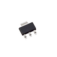
DCY(SOT-223,
3)
6.5mm × 7mm
KVU(TO-252,3)
6.6mm × 10.11mm
如需更多信息,请参阅机械、封装和可订购信息。
封装尺寸(长 × 宽)为标称值,并包括引脚(如适用)。
UA78M
VIN
VOUT
INPUT
CIN
0.33µF
OUTPUT
COMMON
COUT
0.1µF
GND
简化版原理图
本资源的原文使用英文撰写。 为方便起见,TI 提供了译文;由于翻译过程中可能使用了自动化工具,TI 不保证译文的准确性。 为确认
准确性,请务必访问 ti.com 参考最新的英文版本(控制文档)。
English Data Sheet: SLVS059
�uA78M
www.ti.com.cn
ZHCSUB8V – JUNE 1976 – REVISED FEBRUARY 2025
Table of Contents
1 特性................................................................................... 1
2 应用................................................................................... 1
3 说明................................................................................... 1
4 Pin Configuration and Functions...................................3
5 Specifications.................................................................. 4
5.1 Absolute Maximum Ratings........................................ 4
5.2 ESD Ratings............................................................... 4
5.3 Recommended Operating Conditions.........................4
5.4 Thermal Information....................................................5
5.5 Electrical Characteristics: UA78M33 (Both
Legacy and New Chip).................................................. 5
5.6 Electrical Characteristics: UA78M05 (Both
Legacy and New Chip).................................................. 6
5.7 Electrical Characteristics: UA78M06C (Legacy
Chip Only)..................................................................... 6
5.8 Electrical Characteristics: UA78M08C (Legacy
Chip Only)..................................................................... 7
5.9 Electrical Characteristics: UA78M09 (Both
Legacy and New Chip).................................................. 7
5.10 Electrical Characteristics: UA78M10 (Both
Legacy and New Chip).................................................. 8
5.11 Electrical Characteristics: UA78M12 (Both
Legacy and New Chip).................................................. 9
2
5.12 Typical Characteristics............................................ 11
6 Detailed Description......................................................13
6.1 Overview................................................................... 13
6.2 Functional Block Diagram......................................... 13
6.3 Feature Description...................................................13
6.4 Device Functional Modes..........................................15
7 Application and Implementation.................................. 16
7.1 Application Information............................................. 16
7.2 Typical Application.................................................... 16
7.3 System Examples..................................................... 21
7.4 Power Supply Recommendations.............................21
7.5 Layout....................................................................... 21
8 Device and Documentation Support............................23
8.1 Device Support......................................................... 23
8.2 接收文档更新通知..................................................... 23
8.3 支持资源....................................................................23
8.4 Trademarks............................................................... 23
8.5 静电放电警告............................................................ 23
8.6 术语表....................................................................... 23
9 Revision History............................................................ 24
10 Mechanical, Packaging, and Orderable
Information.................................................................... 24
Copyright © 2025 Texas Instruments Incorporated
提交文档反馈
Product Folder Links: uA78M
English Data Sheet: SLVS059
�uA78M
www.ti.com.cn
ZHCSUB8V – JUNE 1976 – REVISED FEBRUARY 2025
OUTPUT
2
COMMON
1
INPUT
3
Thermal
Pad
3
COMMON
COMMON
4 Pin Configuration and Functions
2
1
图 4-1. DCY Package, 3-Pin SOT-223
(Top View)
OUTPUT
COMMON
INPUT
图 4-2. KVU Package, 3-Pin TO-252
(Top View)
表 4-1. Pin Functions
PIN
NAME
NO.
TYPE
DESCRIPTION
COMMON
2
—
Ground
INPUT
1
I
Input pin. Use the recommended capacitor value as listed in the
Recommended Operating Conditions table. Place the input capacitor as
close to the INPUT and COMMON pins of the device as possible.
OUTPUT
3
O
Output pin. Use the recommended capacitor value as listed in the
Recommended Operating Conditions table. Place the output capacitor as
close to the OUTPUT and COMMON pins of the device as possible.
Copyright © 2025 Texas Instruments Incorporated
提交文档反馈
3
Product Folder Links: uA78M
English Data Sheet: SLVS059
�uA78M
www.ti.com.cn
ZHCSUB8V – JUNE 1976 – REVISED FEBRUARY 2025
5 Specifications
5.1 Absolute Maximum Ratings
over operating temperature range (unless otherwise noted)(1)
MIN
MAX
UNIT
Input voltage, VI (for Legacy Chip)
UA78M33C, UA78M33I, UA78M05C, UA78M05I, UA78M06C,
UA78M08C, UA78M09C, UA78M10C, UA78M12C
35
V
Input voltage, VI (for New Chip)
UA78M33C, UA78M33I, UA78M05C, UA78M05I, UA78M09C,
UA78M10C, UA78M12C
45
V
Output voltage, Vo (for New Chip)
-0.3
Junction temperature, TJ
Storage temperature, Tstg
(1)
–65
12
V
150
°C
150
°C
Stresses beyond those listed under Absolute Maximum Ratings may cause permanent damage to the device. These are stress ratings
only, and functional operation of the device at these or any other conditions beyond those indicated under Recommended Operating
Conditions is not implied. Exposure to absolute-maximum-rated conditions for extended periods may affect device reliability.
5.2 ESD Ratings
VALUE
V(ESD)
(1)
(2)
Electrostatic discharge
Human body model (HBM), per ANSI/ESDA/JEDEC JS-001, all
pins(1)
UNIT
2500
Charged device model (CDM), per JEDEC specification JESD22-C101, all pins(2)
V
2000
JEDEC document JEP155 states that 500-V HBM allows safe manufacturing with a standard ESD control process.
JEDEC document JEP157 states that 250-V CDM allows safe manufacturing with a standard ESD control process.
5.3 Recommended Operating Conditions
over operating free-air temperature range (unless otherwise noted)(1)
MIN
VIN
CIN
Input voltage
(2)
Input capacitor
Output capacitor (4)
IO
Output current
25
UA78M33C, UA78M33I (New chip)
5.3
30
UA78M05C, UA78M05I (Legacy chip)
7
25
UA78M05C, UA78M05I (New chip)
7
30
UA78M06 (Legacy chip)
8
25
UA78M08 (Legacy chip)
10.5
25
UA78M09 (Legacy chip)
11.5
26
UA78M09 (New chip)
11.5
30
UA78M10 (Legacy chip)
12.5
28
UA78M10 (New chip)
12.5
30
UA78M12 (Legacy chip)
14.5
30
UA78M12 (New chip)
14.5
30
0.33
0.1
UA78MxxC (Legacy chip)
TJ
(1)
(2)
(3)
(4)
4
Operating junction temperature
MAX
5.3
(3)
COUT (2)
TYP
UA78M33C , UA78M33I (Legacy chip)
UNIT
V
µF
470
µF
500
mA
0
125
UA78MxxI (Legacy chip)
–40
125
UA78MxxC , UA78MxxI (New chip)
–40
125
°C
All voltages are with respect to GND.
UA78M regulator does not need any external capacitors for LDO stability.
An input capacitor with value of 0.33 μF is recommended to counteract the effect of source resistance and inductance, which can in
some cases cause symptoms of system level instability such as ringing or oscillation, especially in the presence of load transients.
An output capacitor with value of 0.1 μF is recommended to improve the load and line transient performance of the UA78M regulator.
The maximum output capacitor is guaranteed by design
Copyright © 2025 Texas Instruments Incorporated
提交文档反馈
Product Folder Links: uA78M
English Data Sheet: SLVS059
�uA78M
www.ti.com.cn
ZHCSUB8V – JUNE 1976 – REVISED FEBRUARY 2025
5.4 Thermal Information
THERMAL METRIC(1)
UA78Mxx
UA78Mxx
UA78Mxx
UA78Mxx
DCY (Legacy
Chip)
DCY (New
Chip)
KCS (Legacy
Chip only)
KVU (Legacy
chip)
KVU (New
chip)
3 PINS
3 PINS
3 PINS
3 PINS
3 PINS
53
77.7
19
30.2
32.1
°C/W
30.6
44.6
17
–
40
°C/W
–
–
3
–
3.3
°C/W
Junction-to-ambient thermal
resistance
RθJA
Rθ
JC(top)
Rθ
JC(bot)
(1)
UA78Mxx
Junction-to-case (top) thermal
resistance
Junction-to-case (bottom) thermal
resistance
UNIT
For more information about traditional and new thermal metrics, see the Semiconductor and IC Package Thermal Metrics application
note.
5.5 Electrical Characteristics: UA78M33 (Both Legacy and New Chip)
specified at TJ = 25°C, VI = 8 V, CIN = 0.33 µF, COUT = 0.1µF, and IO = 350 mA (unless otherwise noted)
TEST CONDITIONS(1)
PARAMETER
MIN
TYP
MAX
3.2
3.3
3.4
Legacy chip
3.1
3.3
3.5
New chip
3.1
3.3
3.5
Legacy chip and new chip
Output voltage
Output voltage line
regulation
VI = 8V to 20V, and IO = 5mA to
TJ = full range
350mA
TJ = –40°C to 125°C
IO = 200mA, VIN = 5.3V to 25V
IO = 200mA, VIN = 8V to 25V
Ripple rejection
VI = 8V to 18V, f = 120Hz
Legacy chip
9
100
28
50
Legacy chip
3
50
New chip
9
20
New chip
IO = 100mA, TJ = full
range
Legacy chip
62
IO = 100mA, TJ = –
40°C to 125°C
New chip
57
Legacy chip
62
80
New chip
56
62
IO = 300mA
Output voltage load
regulation
VI = 8V and IO = 5mA to
500mA
Temperature coefficient of
IO = 5mA
output voltage
Output noise voltage
f = 10 Hz to 100 KHz
Dropout voltage
VI = 8V to 25V, IO = 200mA
Bias current change
IO = 5 mA to 350mA
Short-circuit output
current
100
20
40
TJ = full range
Legacy chip
–1
TJ = –40°C to 125°C
New chip
–1
40
200
New chip
80
200
Legacy chip and new chip
2.0
3.5
mV
6
4.5
6
TJ = full range
Legacy chip
0.8
TJ = –40°C to 125°C
New chip
0.8
TJ = full range
Legacy chip
0.5
TJ = –40°C to 125°C
New chip
0.5
300
VI = 30V
New chip
400
Legacy chip
700
New chip
735
µVrms
V
4.5
Legacy chip
mV
mV/°C
Legacy chip
VI = 35V
Peak output current
(1)
20
New chip
New chip
V
dB
Legacy chip
Legacy chip
Bias current
UNIT
mA
mA
mA
mA
Pulse-testing techniques maintain TJ as close to TA as possible. Thermal effects must be taken into account separately.
Copyright © 2025 Texas Instruments Incorporated
提交文档反馈
5
Product Folder Links: uA78M
English Data Sheet: SLVS059
�uA78M
www.ti.com.cn
ZHCSUB8V – JUNE 1976 – REVISED FEBRUARY 2025
5.6 Electrical Characteristics: UA78M05 (Both Legacy and New Chip)
specified at TJ = 25°C, VI = 10V, CIN = 0.33 µF, COUT = 0.1µF, and IO = 350mA (unless otherwise noted)
TEST CONDITIONS(1)
PARAMETER
Output voltage
Output voltage line
regulation
VI = 7V to 20V, and IO = 5mA to Legacy chip and new chip
350mA
TJ = full range
Legacy chip
VI = 7.2V to 20V, and IO = 5mA
to 350mA
TJ = –40°C to 125°C
IO = 200mA, VIN = 7V to 25V
Legacy chip
IO = 200mA, VIN = 7.2V to 25V
New chip
VI = 8V to 18V, f = 120Hz
IO = 5mA to 500mA
5.25
4.75
5.25
3
100
13
30
1
50
13
30
Legacy chip
62
IO = 100mA, TJ = –
40°C to 125°C
New chip
56
Legacy chip
62
80
New chip
52
58
Legacy chip
20
100
New chip
25
60
Legacy chip
10
50
5
20
TJ = full range
Legacy chip
–1
TJ = –40°C to 125°C
New chip
–1
200
New chip
120
200
Legacy chip and new chip
2.0
New chip
VI = 8V to 25V, IO = 200mA
Bias current change
IO = 5 mA to 350mA
3.5
mV
mV
µVrms
V
4.5
6
4.5
6
TJ = full range
Legacy chip
0.8
TJ = –40°C to 125°C
New chip
0.8
TJ = full range
Legacy chip
0.5
TJ = –40°C to 125°C
New chip
mA
mA
0.5
VI = 35V
Legacy chip
300
VI = 30V
New chip
400
Legacy chip
700
New chip
760
Peak output current
V
mV/°C
40
Legacy chip
Bias current
UNIT
dB
Legacy chip
f = 10 Hz to 100 kHz
Dropout voltage
(1)
4.75
New chip
Temperature coefficient
IO = 5mA
of output voltage
Short-circuit output
current
5.2
New chip
IO = 5mA to 200mA
Output noise voltage
MAX
5
IO = 100mA, TJ = full
range
IO = 300mA
Output voltage load
regulation
TYP
4.8
Legacy chip
IO = 200mA, VIN = 8V to 25V
Ripple rejection
New chip
MIN
mA
mA
Pulse-testing techniques maintain TJ as close to TA as possible. Thermal effects must be taken into account separately.
5.7 Electrical Characteristics: UA78M06C (Legacy Chip Only)
specified at TJ = 25°C, VI = 11V, CIN = 0.33 µF, COUT = 0.1µF, and IO = 350mA (unless otherwise noted)
TEST CONDITIONS(1)
PARAMETER
6
MIN
TYP
5.75
6
MAX UNIT
6.25
Output voltage
VI = 8V to 21V, and IO = 5mA to 350mA
Output voltage line
regulation
IO = 200mA, VIN = 8V to 25V
5
100
IO = 200mA, VIN = 9V to 25V
1.5
50
Ripple rejection
VI = 8V to 18V, f = 120Hz
TJ = 0°C to 125°C
5.7
IO = 100mA, TJ = 0°C to 125°C
59
IO = 300mA
59
6.3
80
V
mV
dB
Copyright © 2025 Texas Instruments Incorporated
提交文档反馈
Product Folder Links: uA78M
English Data Sheet: SLVS059
�uA78M
www.ti.com.cn
ZHCSUB8V – JUNE 1976 – REVISED FEBRUARY 2025
5.7 Electrical Characteristics: UA78M06C (Legacy Chip Only) (续)
specified at TJ = 25°C, VI = 11V, CIN = 0.33 µF, COUT = 0.1µF, and IO = 350mA (unless otherwise noted)
TEST CONDITIONS(1)
PARAMETER
Output voltage load
regulation
MIN
TYP
IO = 5mA to 500mA
20
120
IO = 5mA to 200mA
10
60
Temperature coefficient of
output voltage
IO = 5mA
Output noise voltage
f = 10 Hz to 100 kHz,
TJ = 0°C to 125°C
Dropout voltage
mV
–1
mV/°C
45
µVrms
2.0
Bias current
3.5
Bias current change
V
4.5
6
VI = 9V to 25V, IO = 200mA
TJ = 0°C to 125°C
0.8
IO = 5 mA to 350mA
TJ = 0°C to 125°C
0.5
Short-circuit output current VI = 35V
VI = 35V
Peak output current
(1)
MAX UNIT
mA
mA
270
mA
700
mA
Pulse-testing techniques maintain TJ as close to TA as possible. Thermal effects must be taken into account separately.
5.8 Electrical Characteristics: UA78M08C (Legacy Chip Only)
specified at TJ = 25°C, VI = 14V, CIN = 0.33 µF, COUT = 0.1µF, and IO = 350mA (unless otherwise noted)
TEST CONDITIONS(1)
PARAMETER
Output voltage
VI = 10.5V to 23V, and IO = 5mA to 350mA
Output voltage line regulation
Ripple rejection
TYP
MAX
7.7
8
8.3
7.6
6
100
IO = 200mA, VIN = 11V to 25V
2
50
IO = 100mA, TJ =
0°C to 125°C
56
IO = 300mA
56
160
IO = 5mA to 200mA
10
80
Output noise voltage
f = 10 Hz to 100 kHz,
TJ = 0°C to 125°C
mV/°C
52
µVrms
2.0
Bias current
4.5
Short-circuit output current
(1)
V
6
VI = 9V to 25V, IO = 200mA
TJ = 0°C to 125°C
0.8
IO = 5 mA to 350mA
TJ = 0°C to 125°C
0.5
VI = 35V
Peak output current
mV
–1
Dropout voltage
Bias current change
mV
dB
25
IO = 5mA
V
80
IO = 5mA to 500mA
Temperature coefficient of
output voltage
UNIT
8.4
IO = 200mA, VIN = 10.5V to 25V
VI = 11V to 21.5V, f = 120Hz
Output voltage load regulation
TJ = 0°C to 125°C
MIN
mA
mA
250
mA
700
mA
Pulse-testing techniques maintain TJ as close to TA as possible. Thermal effects must be taken into account separately.
5.9 Electrical Characteristics: UA78M09 (Both Legacy and New Chip)
at specified junction temperature, VI = 16 V, CIN = 0.33 µF, COUT = 0.1µF, and IO = 350 mA (unless otherwise noted)
TEST CONDITIONS(1)
PARAMETER
Output voltage
Output voltage line
regulation
VI = 11.5V to 24V, and IO = 5mA
to 350mA
TJ = 0°C to 125°C
IO = 200mA, VIN = 11.5V to 26V
IO = 200mA, VIN = 12V to 26V
Legacy chip
and new chip
MIN
TYP
MAX
8.6
9
9.4
8.5
9.5
Legacy chip
6
100
New chip
6
30
Legacy chip
2
50
New chip
2
25
Copyright © 2025 Texas Instruments Incorporated
UNIT
V
mV
提交文档反馈
7
Product Folder Links: uA78M
English Data Sheet: SLVS059
�uA78M
www.ti.com.cn
ZHCSUB8V – JUNE 1976 – REVISED FEBRUARY 2025
5.9 Electrical Characteristics: UA78M09 (Both Legacy and New Chip) (续)
at specified junction temperature, VI = 16 V, CIN = 0.33 µF, COUT = 0.1µF, and IO = 350 mA (unless otherwise noted)
TEST CONDITIONS(1)
PARAMETER
IO = 100mA, TJ = 0°C
to 125°C
Ripple rejection
VI = 13V to 23V, f = 120Hz
IO = 300mA
Output voltage load
regulation
IO = 5mA to 500mA
IO = 5mA to 200mA
Output noise voltage
f = 10 Hz to 100 kHz
MIN
Legacy chip
56
New chip
48
Legacy chip
56
80
New chip
48
80
MAX
UNIT
dB
Legacy chip
25
180
New chip
25
90
Legacy chip
10
90
New chip
10
45
Legacy chip
58
New chip
Temperature coefficient
IO = 5mA
of output voltage
TYP
mV
µVrms
230
Legacy chip
and new chip
-1
mV/°C
Dropout voltage
Legacy chip
and new chip
2.0
V
Bias current
Legacy chip
and new chip
4.6
TJ = 0°C to 125°C
VI = 11.5V to 26V, IO = 200mA
TJ = 0°C to 125°C
Legacy chip
and new chip
0.8
IO = 5 mA to 350mA
TJ = 0°C to 125°C
Legacy chip
and new chip
0.5
Bias current change
Short-circuit output
current
mA
mA
VI = 35V
Legacy chip
250
VI = 30V
New chip
400
Legacy chip
700
New chip
760
Peak output current
(1)
6
mA
mA
Pulse-testing techniques maintain TJ as close to TA as possible. Thermal effects must be taken into account separately.
5.10 Electrical Characteristics: UA78M10 (Both Legacy and New Chip)
at specified junction temperature, VI = 17 V, CIN = 0.33 µF, COUT = 0.1µF, and IO = 350 mA (unless otherwise noted)
TEST CONDITIONS(1)
PARAMETER
Output voltage
VI = 12.5V to 25V, and IO =
5mA to 350mA
TJ = 0°C to 125°C
IO = 200mA, VIN = 12.5V to 28V
Output voltage line regulation
IO = 200mA, VIN = 14V to 28V
Ripple rejection
VI = 15V to 25V, f = 120Hz
TYP MAX
10
9.5
Legacy chip
7
100
New chip
7
35
Legacy chip
2
50
2
30
59
Legacy chip
55
80
New chip
45
80
Output voltage load regulation
IO = 5mA to 200mA
45
25
200
New chip
25
120
Legacy chip
10
100
New chip
10
50
New chip
64
255
UNIT
V
mV
dB
Legacy chip
Legacy chip
f = 10 Hz to 100 kHz
10.4
10.5
IO = 100mA, TJ = 0°C Legacy chip
to 125°C
New chip
IO = 5mA to 500mA
8
Legacy chip and new
chip
9.6
New chip
IO = 300mA
Output noise voltage
MIN
mV
µVrms
Copyright © 2025 Texas Instruments Incorporated
提交文档反馈
Product Folder Links: uA78M
English Data Sheet: SLVS059
�uA78M
www.ti.com.cn
ZHCSUB8V – JUNE 1976 – REVISED FEBRUARY 2025
5.10 Electrical Characteristics: UA78M10 (Both Legacy and New Chip) (续)
at specified junction temperature, VI = 17 V, CIN = 0.33 µF, COUT = 0.1µF, and IO = 350 mA (unless otherwise noted)
TEST CONDITIONS(1)
PARAMETER
Temperature coefficient of
output voltage
MIN
TYP MAX
UNIT
Legacy chip and new
chip
-1
mV/°C
Dropout voltage
Legacy chip and new
chip
2.0
V
Bias current
Legacy chip and new
chip
4.7
Bias current change
Short-circuit output current
IO = 5mA
TJ = 0°C to 125°C
VI = 12.5V to 28V, IO =
200mA
TJ = 0°C to 125°C
Legacy chip and new
chip
0.8
IO = 5 mA to 350mA
TJ = 0°C to 125°C
Legacy chip and new
chip
0.5
mA
mA
VI = 35V
Legacy chip
245
VI = 30V
New chip
400
Legacy chip
700
New chip
760
Peak output current
(1)
6
mA
mA
Pulse-testing techniques maintain TJ as close to TA as possible. Thermal effects must be taken into account separately.
5.11 Electrical Characteristics: UA78M12 (Both Legacy and New Chip)
at specified at TJ = 25°C, VI = 19V, CIN = 0.33µF, COUT = 0.1µF and IO = 350mA (unless otherwise noted)
TEST CONDITIONS(1)
PARAMETER
Output voltage
VI = 14.5V to 27V, and IO =
5mA to 350mA
TJ = 0°C to 125°C
IO = 200mA, VIN = 14.5V to 30V
Output voltage line regulation
IO = 200mA, VIN = 16V to 30V
VI = 15V to 25V, f = 120Hz
IO = 300mA
IO = 5mA to 500mA
Output voltage load regulation
IO = 5mA to 200mA
Temperature coefficient of
output voltage
IO = 5mA
Output noise voltage
f = 10Hz to 100kHz
TYP
MAX
12
12.5
11.4
TJ = 0°C to 125°C
8
100
New chip
8
40
Legacy chip
2
50
2
35
Legacy chip
55
New chip
42
Legacy chip
55
80
New chip
42
80
25
240
New chip
25
120
Legacy chip
10
120
New chip
10
60
Legacy chip and
new chip
-1
300
Dropout voltage
Legacy chip and
new chip
2.0
Bias current
Legacy chip and
new chip
4.8
Short-circuit output current
V
6
0.8
IO = 5mA to 350mA
Legacy chip and
new chip
0.5
VI = 35V
Legacy chip
240
VI = 30V
New chip
400
TJ = 0°C to 125°C
Copyright © 2025 Texas Instruments Incorporated
mV
µVrms
Legacy chip and
new chip
Bias current change
mV
mV/°C
75
New chip
VI = 14.5V to 30V, IO = 200mA
V
dB
Legacy chip
Legacy chip
UNIT
12.6
Legacy chip
New chip
IO = 100mA,TJ = 0°C
to 125°C
Ripple rejection
Legacy chip and
new chip
MIN
11.5
mA
mA
mA
提交文档反馈
9
Product Folder Links: uA78M
English Data Sheet: SLVS059
�uA78M
www.ti.com.cn
ZHCSUB8V – JUNE 1976 – REVISED FEBRUARY 2025
5.11 Electrical Characteristics: UA78M12 (Both Legacy and New Chip) (续)
at specified at TJ = 25°C, VI = 19V, CIN = 0.33µF, COUT = 0.1µF and IO = 350mA (unless otherwise noted)
PARAMETER
TEST CONDITIONS(1)
MIN
TYP
Peak output current
Legacy chip
700
Peak output current
New chip
760
(1)
10
MAX
UNIT
mA
Pulse-testing techniques maintain TJ as close to TA as possible. Thermal effects must be taken into account separately.
Copyright © 2025 Texas Instruments Incorporated
提交文档反馈
Product Folder Links: uA78M
English Data Sheet: SLVS059
�uA78M
www.ti.com.cn
ZHCSUB8V – JUNE 1976 – REVISED FEBRUARY 2025
5.12 Typical Characteristics
5.03
6
Vout
5.5
5.02
5
4.5
5.01
3.5
VOUT (V)
VOUT (V)
4
3
2.5
2
4.99
4.98
4.97
1.5
5mA
350mA
500mA
1
0.5
0
-55
5
4.96
4.95
-25
5
35
65
Te mperature (C)
95
125
0
150
50
100
VOUT = 5V, VIN = 8V
150
200 250 300
IOUT (mA)
350
400
450
500
VOUT = 5V, VIN = 8V
图 5-1. Output Voltage vs Temperature (New Chip)
图 5-2. Load Regulation at TJ = 25°C (New Chip)
15
6
5.5
12.5
5
4.5
4
IBIAS (mA)
VOUT (mV)
10
7.5
5
3.5
3
2.5
2
1.5
2.5
5mA
350mA
500mA
1
0.5
0
7.5
10
12.5
15
17.5
20
VIN (V)
22.5
25
27.5
0
10
30
12
14
16
18
20
22
VIN (V)
24
26
28
30
VOUT = 5V, IOUT = 350mA
图 5-3. Line Regulation at TJ = 25°C (New Chip)
图 5-4. Bias Current vs Input Voltage at TJ = 25°C
(New Chip)
1400
6
-55 °C
-40 °C
5.5
1200
5
Current Limit (mA)
4.5
IBIAS (mA)
4
3.5
3
2.5
2
1.5
5mA
350mA
500mA
1
0.5
0
-55
-25
5
35
65
Te mperature (C)
95
125
150
0 °C
25 °C
85 °C
125 °C
150 °C
1000
800
600
400
200
0
5
VOUT = 5V, VIN = 10V
10
15
20
VIN - VOUT
25
30
35
VO = 0V
图 5-5. Bias Current vs Temperature (New Chip)
Copyright © 2025 Texas Instruments Incorporated
图 5-6. ICL vs Input Voltage (New Chip)
提交文档反馈
11
Product Folder Links: uA78M
English Data Sheet: SLVS059
�uA78M
www.ti.com.cn
ZHCSUB8V – JUNE 1976 – REVISED FEBRUARY 2025
5.12 Typical Characteristics (continued)
5
7
-55 °C
-40 °C
0 °C
25 °C
85 °C
125 °C
150 °C
-55 °C
-40 °C
6
4
0 °C
25 °C
85 °C
125 °C
150 °C
3
VOUT (V)
VOUT (V)
5
2
4
3
2
1
1
0
0
0
100
200
300
400 500 600 700
Current Limit (mA)
800
900 1000
0
100
200
300
400 500 600 700
Current Limit (mA)
VO = 3.3V
900 1000
VO = 5V
图 5-7. Output Voltage vs ICL (New Chip)
图 5-8. Output Voltage vs ICL (New Chip)
90
Power Supply Rejection Ratio (dB)
120
100
Ripple Rejection (db)
800
80
60
40
Iout at 100 mA
20
Iout at 300 mA
0
120Hz
240Hz
500Hz
70
60
50
40
30
1x101
1KHz
Frequency
5mA
100mA
300mA
80
1x10²
1x10³
1x10⁴
Frequency (Hz)
C002
VI = 8V to 18V, TJ = 25°C
1x10⁵
1x10⁶
VI = 13V, VO = 5V
图 5-9. PSRR vs Frequency and IO (Legacy Chip)
图 5-10. PSRR vs Frequency and IO (New Chip)
Noise Spectral Density (V/Hz)
2
1
0.7
0.5
0.3
0.2
0.1
0.07
0.05
0.03
0.02
Integrated Noise
(10Hz to 100KHz) : 127
V
0.01
1x101
1x10²
1x10³
1x10⁴
1x10⁵
Frequency (Hz)
1x10⁶
1x10⁷
VIN = 10V, VOUT = 5V, IOUT = 100mA, COUT = 0.1μF
图 5-11. Noise vs Frequency (New Chip)
12
Copyright © 2025 Texas Instruments Incorporated
提交文档反馈
Product Folder Links: uA78M
English Data Sheet: SLVS059
�uA78M
www.ti.com.cn
ZHCSUB8V – JUNE 1976 – REVISED FEBRUARY 2025
6 Detailed Description
6.1 Overview
The UA78M fixed-voltage, integrated-circuit voltage regulator is designed for a wide range of applications. The
UA78M supports a wide range of input voltages and delivers 500mA of load current.
This device features internal current-limiting and thermal shutdown mechanisms. To provide reliable operation
across wide VI ranges, the current-limiting mechanism modulates the load current capacity both by monitoring
the VO level and the difference between the VI and VO voltage levels. The operating ambient temperature range
of the device is –40°C to +125°C for all variants.
6.2 Functional Block Diagram
INPUT
Voltage
Reference
–
+
Over Current
Protection
Temperature
Protection
OUTPUT
COMMON
6.3 Feature Description
6.3.1 Current Limit
The device has an internal current-limit circuit that protects the regulator during transient high-load current faults
or shorting events. In a high-load current fault, the current limit scheme limits the output current to the current
limit (ICL). ICL is listed in the Electrical Characteristics table.
The output voltage is not regulated when the device is in current limit. When a current-limit event occurs, the
device begins to heat up because of the increase in power dissipation. When the device is in current limit, the
pass transistor dissipates power [(VI – VO) × ICL]. For more information on current limits, see the Know Your
Limits application note.
Copyright © 2025 Texas Instruments Incorporated
提交文档反馈
13
Product Folder Links: uA78M
English Data Sheet: SLVS059
�uA78M
www.ti.com.cn
ZHCSUB8V – JUNE 1976 – REVISED FEBRUARY 2025
To achieve a safe operation across a wide range of Input voltage, the UA78M also has a built-in protection
mechanism with current limit. The protection mechanism decreases the current limit as input-to-output voltage
increases and keeps the power transistor inside a safe operating region for all values of input-to-output voltage.
This protection is designed to provide some output current at all values of input-to-output voltage limits defined in
the Recommended Operating Conditions table. 图 6-1 shows the behavior of the current limit variation.
1400
-55 °C
-40 °C
Current Limit (mA)
1200
0 °C
25 °C
85 °C
125 °C
150 °C
1000
800
600
400
200
0
5
10
15
20
VIN - VOUT
25
30
35
图 6-1. Current-Limit vs VHead-room Behavior (New Chip)
6.3.2 Dropout Voltage (VDO)
Dropout voltage (VDO) is defined as the input voltage minus the output voltage (VI – VO) at the rated output
current (IRATED), where the pass transistor is fully on. IRATED is the maximum IO listed in the Recommended
Operating Conditions table. In dropout operation, the pass transistor is in the ohmic or triode region of operation,
and acts as a switch. The dropout voltage indirectly specifies a minimum input voltage greater than the nominal
programmed output voltage at which the output voltage is expected to stay in regulation. If the input voltage falls
to less than the value required to maintain output regulation, then the output voltage falls as well.
6.3.3 Thermal Shutdown
The device contains a thermal shutdown protection circuit to disable the device when the junction temperature
(TJ) of the pass transistor rises to TSD(shutdown) (typical). Thermal shutdown hysteresis makes sure that the
device resets (turns on) when the temperature falls to TSD(reset) (typical).
The thermal time-constant of the semiconductor die is fairly short, thus the device can cycle on and off when
thermal shutdown is reached until power dissipation is reduced. Power dissipation during start-up can be high
from large VI – VO voltage drops across the device or from high inrush currents charging large output
capacitors. Under some conditions, the thermal shutdown protection disables the device before start-up
completes.
For reliable operation, limit the junction temperature to the maximum listed in the Recommended Operating
Conditions table. Operation above this maximum temperature causes the device to exceed operational
specifications. Although the internal protection circuitry of the device is designed to protect against thermal
overall conditions, this circuitry is not intended to replace proper heat sinking. Continuously running the device
into thermal shutdown or above the maximum recommended junction temperature reduces long-term reliability.
14
Copyright © 2025 Texas Instruments Incorporated
提交文档反馈
Product Folder Links: uA78M
English Data Sheet: SLVS059
�uA78M
www.ti.com.cn
ZHCSUB8V – JUNE 1976 – REVISED FEBRUARY 2025
6.4 Device Functional Modes
表 6-1 provides a quick comparison between the normal and dropout modes of operation.
表 6-1. Device Functional Mode Comparison
OPERATING MODE
PARAMETER
VI
IO
Normal
VI > VOUT(nom) + VDO
IO < ICL
Dropout
VI < VOUT(nom) + VDO
IO < ICL
6.4.1 Normal Operation
The device regulates to the nominal output voltage under the following conditions:
• The input voltage is greater than the nominal output voltage plus the dropout voltage (VOUT(nom) + VDO)
• The output current is less than the current limit (IO < ICL)
• The device junction temperature is greater than –40°C and less than +125°C
6.4.2 Dropout Operation
If the input voltage is lower than the nominal output voltage plus the specified dropout voltage, but all other
conditions are met for normal operation, the device operates in dropout mode. In this mode, the output voltage
tracks the input voltage. During this mode, the transient performance of the device becomes significantly
degraded because the pass transistor is in the ohmic or triode region, and acts as a switch. Line or load
transients in dropout can result in large output voltage deviations.
When the device is in a steady dropout state (defined as when the device is in dropout, VI < VOUT(NOM) + VDO,
directly after being in a normal regulation state, but not during start up), the pass transistor is driven into the
ohmic or triode region. When the input voltage returns to a value greater than or equal to the nominal output
voltage plus the dropout voltage (VOUT(NOM) + VDO), the output voltage can overshoot for a short period of time
while the device pulls the pass transistor back into the linear region.
Copyright © 2025 Texas Instruments Incorporated
提交文档反馈
15
Product Folder Links: uA78M
English Data Sheet: SLVS059
�uA78M
www.ti.com.cn
ZHCSUB8V – JUNE 1976 – REVISED FEBRUARY 2025
7 Application and Implementation
备注
以下应用部分中的信息不属于 TI 器件规格的范围,TI 不担保其准确性和完整性。TI 的客 户应负责确定
器件是否适用于其应用。客户应验证并测试其设计,以确保系统功能。
7.1 Application Information
The UA78M is designed for use as a linear regulator with only a few external components needed. Use the
UA78M to clean power-supply noise by attenuating ripple on the input signal.
7.2 Typical Application
The UA78M is typically used as a fixed-output linear regulator, sourcing current up to 500mA into a load.
UA78M
VIN
VOUT
INPUT
OUTPUT
COMMON
CIN
0.33µF
COUT
0.1µF
GND
图 7-1. Fixed-Output Regulator
7.2.1 Design Requirements
Tie the COMMON pin to ground to set the OUTPUT pin to the desired fixed output voltage.
Although not required, a 0.33µF bypass capacitor is recommended on the input, and a 0.1µF bypass capacitor is
recommend on the output.
7.2.2 Detailed Design Procedure
7.2.2.1 Input and Output Capacitor Requirements
Although the input and output capacitors are not required for stability, good analog design practice is to connect
a capacitor from INPUT to COMMON and from OUTPUT to COMMON. The input capacitor counteracts reactive
input sources and improves transient response, input ripple, and PSRR. Use an input capacitor if the source
impedance is more than 0.5Ω. A higher value capacitor can be necessary if large, fast rise-time load or line
transients are anticipated or if the device is located several inches from the input power source.
Dynamic performance of the device is improved by using a large output capacitor. Use an output capacitor within
the range specified in the Recommended Operating Conditions table for stability.
7.2.2.2 Power Dissipation (PD)
Circuit reliability requires consideration of the device power dissipation, location of the circuit on the printed
circuit board (PCB), and correct sizing of the thermal plane. Make sure the PCB area around the regulator has
few or no other heat-generating devices that cause added thermal stress.
To first-order approximation, power dissipation in the regulator depends on the input-to-output voltage difference
and load conditions. The following equation calculates power dissipation (PD).
(1)
PD = (VI – VO) × IO
16
Copyright © 2025 Texas Instruments Incorporated
提交文档反馈
Product Folder Links: uA78M
English Data Sheet: SLVS059
�uA78M
www.ti.com.cn
ZHCSUB8V – JUNE 1976 – REVISED FEBRUARY 2025
备注
Power dissipation is minimized, and therefore greater efficiency be achieved, by correct selection of
the system voltage rails. For the lowest power dissipation, use the minimum input voltage required for
correct output regulation.
For devices with a thermal pad, the primary heat conduction path for the device package is through the thermal
pad to the PCB. Solder the thermal pad to a copper pad area under the device. This pad area contains an array
of plated vias that conduct heat to additional copper planes for increased heat dissipation.
The maximum power dissipation determines the maximum allowable ambient temperature (TA) for the device.
According to the following equation, power dissipation and junction temperature are most often related by the
junction-to-ambient thermal resistance (RθJA) of the combined PCB and device package and the temperature of
the ambient air (TA).
(2)
TJ = TA + (RθJA × PD)
Thermal resistance (RθJA) is highly dependent on the heat-spreading capability built into the particular PCB
design, and therefore varies according to the total copper area, copper weight, and location of the planes. The
junction-to-ambient thermal resistance listed in the Thermal Information table is determined by the JEDEC
standard PCB and copper-spreading area, and is used as a relative measure of package thermal performance.
As mentioned in the An empirical analysis of the impact of board layout on LDO thermal performance application
note, RθJA is improved by 35% to 55% compared to the Thermal Information table value with the PCB board
layout optimization.
7.2.2.3 Estimating Junction Temperature
The JEDEC standard now recommends the use of psi (Ψ) thermal metrics to estimate the junction temperatures
of the linear regulator when in circuit on a typical PCB board application. These metrics are not thermal
resistance parameters and instead offer a practical and relative way to estimate junction temperature. These psi
metrics are determined to be significantly independent of the copper area available for heat-spreading. The
Thermal Information table lists the primary thermal metrics, which are the junction-to-top characterization
parameter (ψJT) and junction-to-board characterization parameter (ψJB). These parameters provide two
methods for calculating the junction temperature (TJ), as described in the following equations. Use the junctionto-top characterization parameter (ψJT) with the temperature at the center-top of device package (TT) to
calculate the junction temperature. Use the junction-to-board characterization parameter (ψJB) with the PCB
surface temperature 1mm from the device package (TB) to calculate the junction temperature.
(3)
TJ = TT + ψJT × PD
where:
• PD is the dissipated power
• TT is the temperature at the center-top of the device package
(4)
TJ = TB + ψJB × PD
where:
• TB is the PCB surface temperature measured 1mm from the device package and centered on the package
edge
For detailed information on the thermal metrics and how to use them, see the Semiconductor and IC Package
Thermal Metrics application note.
7.2.2.4 External Capacitor Requirements
The UA78M is designed to be stable without any external component. Multilayer ceramic capacitors have
become the industry standard for these types of applications and are recommended, but use good judgment.
Copyright © 2025 Texas Instruments Incorporated
提交文档反馈
17
Product Folder Links: uA78M
English Data Sheet: SLVS059
�uA78M
www.ti.com.cn
ZHCSUB8V – JUNE 1976 – REVISED FEBRUARY 2025
Ceramic capacitors that employ X7R-, X5R-, and C0G-rated dielectric materials provide relatively good
capacitive stability across temperature, whereas the use of Y5V-rated capacitors is discouraged because of
large variations in capacitance.
Regardless of the ceramic capacitor type selected, the effective capacitance varies with operating voltage and
temperature. Generally, expect the effective capacitance to decrease by as much as 50%. The input and output
capacitors recommended in the Recommended Operating Conditions table account for an effective capacitance
of approximately 50% of the nominal value.
7.2.2.5 Overload Recovery
As the input voltage rises when power is first turned on, the output follows the input, allowing the regulator to
start up into very heavy loads. The input-to-output voltage differential is small during start up when the input
voltage is rising, allowing the regulator to supply large output currents. With a high input voltage, a problem
occurs where removing an output short does not allow the output voltage to recover. Other regulators also
exhibit this phenomenon, so the behavior is not unique to the UA78M.
The problem occurs with a heavy output load when the input voltage is high and the output voltage is low.
Common situations occur immediately when removing a short circuit after the input voltage is already turned on.
The load line for such a load has the possibility to intersect the output current curve at two points. If this condition
happens, there are two stable output operating points for the regulator. With this double intersection, the input
power supply is potentially cycled down to zero and brought up again to make the output recover to the desired
voltage operating point.
7.2.2.6 Reverse Current
Excessive reverse current can damage this device. Reverse current flows through the emitter-base junction of
the pass transistor instead of the normal conducting channel. At high magnitudes, this current flow degrades the
long-term reliability of the device.
Conditions where reverse current can occur are outlined in this section, all of which can exceed the absolute
maximum rating of VO ≤ VI + 7V. These conditions are:
• If the device has a large COUT and the input supply collapses with little or no load current
• The output is biased when the input supply is not established
• The output is biased above the input supply
If reverse current flow is expected in the application, use external protection to protect the device. Reverse
current is not limited in the device, so external limiting is required if extended reverse voltage operation is
anticipated. Limit reverse current to 5% or less of the rated output current of the device in the event this current
cannot be avoided.
18
Copyright © 2025 Texas Instruments Incorporated
提交文档反馈
Product Folder Links: uA78M
English Data Sheet: SLVS059
�uA78M
www.ti.com.cn
ZHCSUB8V – JUNE 1976 – REVISED FEBRUARY 2025
图 7-2 shows one approach for protecting the device.
Schottky Diode
Internal Body Diode
INPUT
OUTPUT
CIN
COUT
COMMON
GND
GND
GND
图 7-2. Example Circuit for Reverse Current Protection Using a Schottky Diode
7.2.2.7 Polarity Reversal Protection
In many applications, a voltage regulator powers a load that is not connected to ground, but instead, is
connected to a voltage source of the opposite polarity (for example, operational amplifiers, level-shifting circuits,
and so on). During start-up and short-circuit events, this connection can lead to polarity reversal of the regulator
output and can damage the internal components of the regulator.
To avoid polarity reversal on the regulator output, use external protection to protect the device.
图 7-3 shows one approach for protecting the device.
+VO
INPUT
OUTPUT
CIN
COUT
COMMON
Schottky
Diode
-VO
GND
图 7-3. Example Circuit for Polarity Reversal Protection Using a Schottky Diode
Copyright © 2025 Texas Instruments Incorporated
提交文档反馈
19
Product Folder Links: uA78M
English Data Sheet: SLVS059
�uA78M
www.ti.com.cn
ZHCSUB8V – JUNE 1976 – REVISED FEBRUARY 2025
7.2.3 Application Curves
5.50
5.00
VOUT (V)
4.75
4.50
4.25
5 mA
500 mA
4.00
6.00
6.25
6.50
6.75
7.00
7.25
7.50
7.75
8.00
Input Voltage (V)
IOUT
IOUT
IOUT
IOUT
4
4.5
5
5.5
C001
VOUT = 5V
8
8.5
9
9.5
3.3
20
3
15
2.7
10
8
5
6
0
4
2.1
VIN (V)
VOUT (V)
7 7.5
VIN (V)
1.8
1.5
1.2
No Load
5mA
350mA
500mA
0.9
0.6
12
VIN
VOUT 10
-5
2
-10
0
-15
-2
-20
-4
-25
0.3
3
3.5
4
4.5
5
5.5
6
VIN (V)
10
图 7-5. VIN vs VOUT at TJ = 25°C (New Chip)
2.4
6.5
7
7.5
0
8
VOUT = 3.3V
100
200
300
400 500 600
Time (s)
700
800
-6
900 1000
VO = 5V, dVIN/dt = 1V/μs, IOUT = 350mA, COUT = 0.1μF
图 7-6. VIN vs VOUT at TJ = 25°C (New Chip)
图 7-7. Line Transient Behavior (New Chip)
1600
IOUT
VOUT
100
1200
50
800
0
400
-50
VOUT (V)
150
IOUT (mA)
6.5
0
5mA
350mA
500mA
VOUT = 5V
图 7-4. VIN vs VOUT at TJ = 25°C (Legacy Chip)
0
-100
-400
-150
0
50
100
150
200
250
Time (s)
300
350
-800
400
VIN = 10V, VOUT = 5V, IOUT = 1mA to 100mA, dI/dt = 1A/μs,
VIN = 0V to 10V, VOUT = 5V, IOUT = 100mA, dVIN/dt = 1V/μs,
COUT = 0.1μF
COUT = 0.1μF
图 7-8. Load Transient Behavior (New Chip)
20
6
=
=
=
=
VOUT (mV)
Output Voltage (V)
5.25
5.1
4.8
4.5
4.2
3.9
3.6
3.3
3
2.7
2.4
2.1
1.8
1.5
1.2
图 7-9. Start-Up (New Chip)
Copyright © 2025 Texas Instruments Incorporated
提交文档反馈
Product Folder Links: uA78M
English Data Sheet: SLVS059
�uA78M
www.ti.com.cn
ZHCSUB8V – JUNE 1976 – REVISED FEBRUARY 2025
7.3 System Examples
7.3.1 Positive Regulator in Negative Configuration
图 7-10 shows the UA78M as a positive regulator used in a negative configuration. Make sure VI floats in this
configuration.
UA78MXX
INPUT
GND
OUTPUT
+
COMMON
VI
-
-VO
图 7-10. Positive Regulator in Negative Configuration
7.3.2 Current Limiter Circuit
图 7-11 shows an example of using the UA78M as a current limiter. The output current limit is set by 方程式 5,
(5)
IO
UA78MXX
VI
INPUT
OUTPUT
COMMON
Output
R1
+ VO(Reg) -
图 7-11. Current Limiter Example
7.4 Power Supply Recommendations
See the Recommended Operating Conditions for the recommended power supply voltages for each variation of
the UA78M. Different orderable part numbers are able to tolerate different levels of voltage. Also, place a
decoupling capacitor on the output to limit noise on the input.
7.5 Layout
7.5.1 Layout Guidelines
Keep trace widths large enough to eliminate problematic I×R voltage drops at the input and output pins. Place
bypass capacitors as close to the UA78M as possible. Additional copper and vias connected to ground facilitate
additional thermal dissipation, preventing the device from reaching thermal overload.
Copyright © 2025 Texas Instruments Incorporated
提交文档反馈
21
Product Folder Links: uA78M
English Data Sheet: SLVS059
�uA78M
www.ti.com.cn
ZHCSUB8V – JUNE 1976 – REVISED FEBRUARY 2025
7.5.2 Layout Example
COMMON
OUTPUT
COMMON
INPUT
PF
Ground
PF
Ground
图 7-12. Layout Diagram
22
Copyright © 2025 Texas Instruments Incorporated
提交文档反馈
Product Folder Links: uA78M
English Data Sheet: SLVS059
�uA78M
www.ti.com.cn
ZHCSUB8V – JUNE 1976 – REVISED FEBRUARY 2025
8 Device and Documentation Support
8.1 Device Support
8.1.1 Development Support
8.1.1.1 Evaluation Module
An evaluation module (EVM) is available to assist in the initial circuit performance evaluation using the UA78L.
The UA78MEVM (and related user guide) can be requested at the Texas Instruments website through the
product folders or purchased directly from the TI eStore.
8.1.2 Device Nomenclature
表 8-1. Device Nomenclature
PRODUCT(1)
UA78Mxxyyyz
(1)
VOUT
xx is the nominal output voltage (for example, 05 = 5.0V, 15 = 15.0V).
yyy is the package designator.
z is the package quantity.
Devices can ship with the legacy chip (CSO: SFB) or the new chip (CSO: RFB). The reel
packaging label provides CSO information to distinguish which chip is being used. Device
performance for new and legacy chips is denoted throughout the data sheet.
For the most current package and ordering information see the Package Option Addendum at the end of this document, or see the TI
website at www.ti.com.
8.2 接收文档更新通知
要接收文档更新通知,请导航至 ti.com 上的器件产品文件夹。点击通知 进行注册,即可每周接收产品信息更改摘
要。有关更改的详细信息,请查看任何已修订文档中包含的修订历史记录。
8.3 支持资源
TI E2E™ 中文支持论坛是工程师的重要参考资料,可直接从专家处获得快速、经过验证的解答和设计帮助。搜索
现有解答或提出自己的问题,获得所需的快速设计帮助。
链接的内容由各个贡献者“按原样”提供。这些内容并不构成 TI 技术规范,并且不一定反映 TI 的观点;请参阅
TI 的使用条款。
8.4 Trademarks
TI E2E™ is a trademark of Texas Instruments.
所有商标均为其各自所有者的财产。
8.5 静电放电警告
静电放电 (ESD) 会损坏这个集成电路。德州仪器 (TI) 建议通过适当的预防措施处理所有集成电路。如果不遵守正确的处理
和安装程序,可能会损坏集成电路。
ESD 的损坏小至导致微小的性能降级,大至整个器件故障。精密的集成电路可能更容易受到损坏,这是因为非常细微的参
数更改都可能会导致器件与其发布的规格不相符。
8.6 术语表
TI 术语表
本术语表列出并解释了术语、首字母缩略词和定义。
Copyright © 2025 Texas Instruments Incorporated
提交文档反馈
23
Product Folder Links: uA78M
English Data Sheet: SLVS059
�uA78M
www.ti.com.cn
ZHCSUB8V – JUNE 1976 – REVISED FEBRUARY 2025
9 Revision History
注:以前版本的页码可能与当前版本的页码不同
Changes from Revision U (May 2024) to Revision V (February 2025)
Page
• 从文档标题中删除了 35V ...................................................................................................................................1
• 更改了特性 部分:已将输入电压范围 要点中的 35V 更改为 30V、添加了绝对最大输入电压 要点,并删除了封
装 要点................................................................................................................................................................1
• 更改了 说明 部分................................................................................................................................................. 1
• Added information of new chip for 9V voltage option......................................................................................... 7
• Added information of new chip for 10V voltage option....................................................................................... 8
• Added information of new chip for 12V voltage option....................................................................................... 9
Changes from Revision T (January 2015) to Revision U (May 2024)
•
•
•
•
Page
更新了整个文档中的表格、图和交叉参考的编号格式.........................................................................................1
更改了整个文档以与当前系列格式保持一致....................................................................................................... 1
向文档添加了 M3 器件........................................................................................................................................1
为了保持一致性,通篇将引脚名称从 IN、GND 和 OUT 更改为 INPUT、COMMON 和 OUTPUT ................... 1
10 Mechanical, Packaging, and Orderable Information
The following pages include mechanical, packaging, and orderable information. This information is the most
current data available for the designated devices. This data is subject to change without notice and revision of
this document. For browser-based versions of this data sheet, refer to the left-hand navigation.
24
Copyright © 2025 Texas Instruments Incorporated
提交文档反馈
Product Folder Links: uA78M
English Data Sheet: SLVS059
�PACKAGE OPTION ADDENDUM
www.ti.com
30-Jun-2025
PACKAGING INFORMATION
Orderable part number
Status
Material type
(1)
(2)
Package | Pins
Package qty | Carrier
RoHS
(3)
Lead finish/
Ball material
MSL rating/
Peak reflow
(4)
(5)
Op temp (°C)
Part marking
(6)
SN78MCDCYR
Active
Production
SOT-223 (DCY) | 4
2500 | LARGE T&R
Yes
SN
Level-2-260C-1 YEAR
0 to 125
C5
UA78M05CDCY
Active
Production
SOT-223 (DCY) | 4
80 | TUBE
Yes
SN
Level-2-260C-1 YEAR
0 to 125
C5
UA78M05CDCY.A
Active
Production
SOT-223 (DCY) | 4
80 | TUBE
Yes
SN
Level-2-260C-1 YEAR
0 to 125
C5
UA78M05CDCYG3
Active
Production
SOT-223 (DCY) | 4
80 | TUBE
Yes
SN
Level-2-260C-1 YEAR
0 to 125
C5
UA78M05CDCYR
Active
Production
SOT-223 (DCY) | 4
2500 | LARGE T&R
Yes
SN
Level-2-260C-1 YEAR
0 to 125
C5
UA78M05CDCYR.A
Active
Production
SOT-223 (DCY) | 4
2500 | LARGE T&R
Yes
SN
Level-2-260C-1 YEAR
0 to 125
C5
UA78M05CDCYRG3
Active
Production
SOT-223 (DCY) | 4
2500 | LARGE T&R
Yes
SN
Level-2-260C-1 YEAR
0 to 125
C5
UA78M05CKCS
Active
Production
TO-220 (KCS) | 3
50 | TUBE
Yes
SN
N/A for Pkg Type
0 to 125
UA78M05C
UA78M05CKCS.A
Active
Production
TO-220 (KCS) | 3
50 | TUBE
Yes
SN
N/A for Pkg Type
0 to 125
UA78M05C
UA78M05CKCSE3
Active
Production
TO-220 (KCS) | 3
50 | TUBE
Yes
SN
N/A for Pkg Type
0 to 125
UA78M05C
UA78M05CKVURG3
Active
Production
TO-252 (KVU) | 3
2500 | LARGE T&R
Yes
SN
Level-3-260C-168 HR
0 to 125
78M05C
UA78M05CKVURG3.A
Active
Production
TO-252 (KVU) | 3
2500 | LARGE T&R
Yes
SN
Level-3-260C-168 HR
0 to 125
78M05C
UA78M05IDCY
Active
Production
SOT-223 (DCY) | 4
80 | TUBE
Yes
SN
Level-2-260C-1 YEAR
-40 to 125
(C5, J5)
UA78M05IDCY.A
Active
Production
SOT-223 (DCY) | 4
80 | TUBE
Yes
SN
Level-2-260C-1 YEAR
-40 to 125
(C5, J5)
UA78M05IDCYG3
Active
Production
SOT-223 (DCY) | 4
80 | TUBE
Yes
SN
Level-2-260C-1 YEAR
-40 to 125
(C5, J5)
UA78M05IDCYR
Active
Production
SOT-223 (DCY) | 4
2500 | LARGE T&R
Yes
SN
Level-2-260C-1 YEAR
-40 to 125
(C5, J5)
(C5, J5)
UA78M05IDCYR.A
Active
Production
SOT-223 (DCY) | 4
2500 | LARGE T&R
Yes
SN
Level-2-260C-1 YEAR
-40 to 125
UA78M05IDCYRG3
Active
Production
SOT-223 (DCY) | 4
2500 | LARGE T&R
Yes
SN
Level-2-260C-1 YEAR
-40 to 125
(C5, J5)
UA78M05IKCS
Active
Production
TO-220 (KCS) | 3
50 | TUBE
Yes
SN
N/A for Pkg Type
-40 to 125
UA78M05I
UA78M05IKCS.A
Active
Production
TO-220 (KCS) | 3
50 | TUBE
Yes
SN
N/A for Pkg Type
-40 to 125
UA78M05I
UA78M05IKCSE3
Active
Production
TO-220 (KCS) | 3
50 | TUBE
Yes
SN
N/A for Pkg Type
-40 to 125
UA78M05I
UA78M05IKVURG3
Active
Production
TO-252 (KVU) | 3
2500 | LARGE T&R
Yes
SN
Level-3-260C-168 HR
-40 to 125
78M05I
UA78M05IKVURG3.A
Active
Production
TO-252 (KVU) | 3
2500 | LARGE T&R
Yes
SN
Level-3-260C-168 HR
-40 to 125
78M05I
UA78M06CKVURG3
Active
Production
TO-252 (KVU) | 3
2500 | LARGE T&R
Yes
SN
Level-3-260C-168 HR
0 to 125
78M06C
UA78M06CKVURG3.A
Active
Production
TO-252 (KVU) | 3
2500 | LARGE T&R
Yes
SN
Level-3-260C-168 HR
0 to 125
78M06C
UA78M08CDCY
Active
Production
SOT-223 (DCY) | 4
80 | TUBE
Yes
SN
Level-2-260C-1 YEAR
0 to 125
C8
UA78M08CDCY.A
Active
Production
SOT-223 (DCY) | 4
80 | TUBE
Yes
SN
Level-2-260C-1 YEAR
0 to 125
C8
UA78M08CDCYG3
Active
Production
SOT-223 (DCY) | 4
80 | TUBE
Yes
SN
Level-2-260C-1 YEAR
0 to 125
C8
UA78M08CDCYR
Active
Production
SOT-223 (DCY) | 4
2500 | LARGE T&R
Yes
SN
Level-2-260C-1 YEAR
0 to 125
C8
Addendum-Page 1
�PACKAGE OPTION ADDENDUM
www.ti.com
Orderable part number
(1)
30-Jun-2025
Status
Material type
(1)
(2)
Package | Pins
Package qty | Carrier
RoHS
(3)
Lead finish/
Ball material
MSL rating/
Peak reflow
(4)
(5)
Op temp (°C)
Part marking
(6)
UA78M08CDCYR.A
Active
Production
SOT-223 (DCY) | 4
2500 | LARGE T&R
Yes
SN
Level-2-260C-1 YEAR
0 to 125
C8
UA78M08CKCS
Active
Production
TO-220 (KCS) | 3
50 | TUBE
Yes
SN
N/A for Pkg Type
0 to 125
UA78M08C
UA78M08CKCS.A
Active
Production
TO-220 (KCS) | 3
50 | TUBE
Yes
SN
N/A for Pkg Type
0 to 125
UA78M08C
UA78M08CKCSE3
Active
Production
TO-220 (KCS) | 3
50 | TUBE
Yes
SN
N/A for Pkg Type
0 to 125
UA78M08C
UA78M08CKVURG3
Active
Production
TO-252 (KVU) | 3
2500 | LARGE T&R
Yes
SN
Level-3-260C-168 HR
0 to 125
78M08C
UA78M08CKVURG3.A
Active
Production
TO-252 (KVU) | 3
2500 | LARGE T&R
Yes
SN
Level-3-260C-168 HR
0 to 125
78M08C
UA78M09CKVURG3
Active
Production
TO-252 (KVU) | 3
2500 | LARGE T&R
Yes
SN
Level-3-260C-168 HR
0 to 125
78M09C
UA78M09CKVURG3.A
Active
Production
TO-252 (KVU) | 3
2500 | LARGE T&R
Yes
SN
Level-3-260C-168 HR
0 to 125
78M09C
UA78M10CKVURG3
Active
Production
TO-252 (KVU) | 3
2500 | LARGE T&R
Yes
SN
Level-3-260C-168 HR
0 to 125
78M10C
UA78M10CKVURG3.A
Active
Production
TO-252 (KVU) | 3
2500 | LARGE T&R
Yes
SN
Level-3-260C-168 HR
0 to 125
78M10C
UA78M12CKCS
Active
Production
TO-220 (KCS) | 3
50 | TUBE
Yes
SN
N/A for Pkg Type
0 to 125
UA78M12C
UA78M12CKCS.A
Active
Production
TO-220 (KCS) | 3
50 | TUBE
Yes
SN
N/A for Pkg Type
0 to 125
UA78M12C
UA78M12CKCSE3
Active
Production
TO-220 (KCS) | 3
50 | TUBE
Yes
SN
N/A for Pkg Type
0 to 125
UA78M12C
UA78M12CKVURG3
Active
Production
TO-252 (KVU) | 3
2500 | LARGE T&R
Yes
SN
Level-3-260C-168 HR
0 to 125
78M12C
UA78M12CKVURG3.A
Active
Production
TO-252 (KVU) | 3
2500 | LARGE T&R
Yes
SN
Level-3-260C-168 HR
0 to 125
78M12C
UA78M33CDCY
Active
Production
SOT-223 (DCY) | 4
80 | TUBE
Yes
SN
Level-2-260C-1 YEAR
0 to 125
C3
UA78M33CDCY.A
Active
Production
SOT-223 (DCY) | 4
80 | TUBE
Yes
SN
Level-2-260C-1 YEAR
0 to 125
C3
UA78M33CDCYG3
Active
Production
SOT-223 (DCY) | 4
80 | TUBE
Yes
SN
Level-2-260C-1 YEAR
0 to 125
C3
UA78M33CDCYR
Active
Production
SOT-223 (DCY) | 4
2500 | LARGE T&R
Yes
SN
Level-2-260C-1 YEAR
0 to 125
C3
UA78M33CDCYR.A
Active
Production
SOT-223 (DCY) | 4
2500 | LARGE T&R
Yes
SN
Level-2-260C-1 YEAR
0 to 125
C3
UA78M33CDCYRG3
Active
Production
SOT-223 (DCY) | 4
2500 | LARGE T&R
Yes
SN
Level-2-260C-1 YEAR
0 to 125
C3
UA78M33CKCS
Active
Production
TO-220 (KCS) | 3
50 | TUBE
Yes
SN
N/A for Pkg Type
0 to 125
UA78M33C
UA78M33CKCS.A
Active
Production
TO-220 (KCS) | 3
50 | TUBE
Yes
SN
N/A for Pkg Type
0 to 125
UA78M33C
UA78M33CKCSE3
Active
Production
TO-220 (KCS) | 3
50 | TUBE
Yes
SN
N/A for Pkg Type
0 to 125
UA78M33C
UA78M33CKVURG3
Active
Production
TO-252 (KVU) | 3
2500 | LARGE T&R
Yes
SN
Level-3-260C-168 HR
0 to 125
78M33C
UA78M33CKVURG3.A
Active
Production
TO-252 (KVU) | 3
2500 | LARGE T&R
Yes
SN
Level-3-260C-168 HR
0 to 125
78M33C
UA78M33IKVURG3
Active
Production
TO-252 (KVU) | 3
2500 | LARGE T&R
Yes
SN
Level-3-260C-168 HR
-40 to 125
78M33I
UA78M33IKVURG3.A
Active
Production
TO-252 (KVU) | 3
2500 | LARGE T&R
Yes
SN
Level-3-260C-168 HR
-40 to 125
78M33I
Status: For more details on status, see our product life cycle.
Addendum-Page 2
�PACKAGE OPTION ADDENDUM
www.ti.com
30-Jun-2025
(2)
Material type: When designated, preproduction parts are prototypes/experimental devices, and are not yet approved or released for full production. Testing and final process, including without limitation quality assurance,
reliability performance testing, and/or process qualification, may not yet be complete, and this item is subject to further changes or possible discontinuation. If available for ordering, purchases will be subject to an additional
waiver at checkout, and are intended for early internal evaluation purposes only. These items are sold without warranties of any kind.
(3)
RoHS values: Yes, No, RoHS Exempt. See the TI RoHS Statement for additional information and value definition.
(4)
Lead finish/Ball material: Parts may have multiple material finish options. Finish options are separated by a vertical ruled line. Lead finish/Ball material values may wrap to two lines if the finish value exceeds the maximum
column width.
(5)
MSL rating/Peak reflow: The moisture sensitivity level ratings and peak solder (reflow) temperatures. In the event that a part has multiple moisture sensitivity ratings, only the lowest level per JEDEC standards is shown.
Refer to the shipping label for the actual reflow temperature that will be used to mount the part to the printed circuit board.
(6)
Part marking: There may be an additional marking, which relates to the logo, the lot trace code information, or the environmental category of the part.
Multiple part markings will be inside parentheses. Only one part marking contained in parentheses and separated by a "~" will appear on a part. If a line is indented then it is a continuation of the previous line and the two
combined represent the entire part marking for that device.
Important Information and Disclaimer:The information provided on this page represents TI's knowledge and belief as of the date that it is provided. TI bases its knowledge and belief on information provided by third parties, and
makes no representation or warranty as to the accuracy of such information. Efforts are underway to better integrate information from third parties. TI has taken and continues to take reasonable steps to provide representative
and accurate information but may not have conducted destructive testing or chemical analysis on incoming materials and chemicals. TI and TI suppliers consider certain information to be proprietary, and thus CAS numbers
and other limited information may not be available for release.
In no event shall TI's liability arising out of such information exceed the total purchase price of the TI part(s) at issue in this document sold by TI to Customer on an annual basis.
OTHER QUALIFIED VERSIONS OF UA78M :
• Automotive : UA78M-Q1
NOTE: Qualified Version Definitions:
• Automotive - Q100 devices qualified for high-reliability automotive applications targeting zero defects
Addendum-Page 3
�PACKAGE MATERIALS INFORMATION
www.ti.com
23-May-2025
TAPE AND REEL INFORMATION
REEL DIMENSIONS
TAPE DIMENSIONS
K0
P1
B0 W
Reel
Diameter
Cavity
A0
B0
K0
W
P1
A0
Dimension designed to accommodate the component width
Dimension designed to accommodate the component length
Dimension designed to accommodate the component thickness
Overall width of the carrier tape
Pitch between successive cavity centers
Reel Width (W1)
QUADRANT ASSIGNMENTS FOR PIN 1 ORIENTATION IN TAPE
Sprocket Holes
Q1
Q2
Q1
Q2
Q3
Q4
Q3
Q4
User Direction of Feed
Pocket Quadrants
*All dimensions are nominal
Device
UA78M05CDCYR
Package Package Pins
Type Drawing
SPQ
SOT-223
Reel
Reel
A0
Diameter Width (mm)
(mm) W1 (mm)
DCY
4
2500
330.0
12.4
B0
(mm)
K0
(mm)
P1
(mm)
W
Pin1
(mm) Quadrant
7.05
7.4
1.9
8.0
12.0
Q3
UA78M05CKVURG3
TO-252
KVU
3
2500
330.0
16.4
6.9
10.5
2.7
8.0
16.0
Q2
UA78M05IDCYR
SOT-223
DCY
4
2500
330.0
12.4
7.05
7.4
1.9
8.0
12.0
Q3
UA78M05IKVURG3
TO-252
KVU
3
2500
330.0
16.4
6.9
10.5
2.7
8.0
16.0
Q2
UA78M06CKVURG3
TO-252
KVU
3
2500
330.0
16.4
6.9
10.5
2.7
8.0
16.0
Q2
UA78M08CDCYR
SOT-223
DCY
4
2500
330.0
12.4
7.05
7.4
1.9
8.0
12.0
Q3
UA78M08CKVURG3
TO-252
KVU
3
2500
330.0
16.4
6.9
10.5
2.7
8.0
16.0
Q2
UA78M09CKVURG3
TO-252
KVU
3
2500
330.0
16.4
6.9
10.5
2.7
8.0
16.0
Q2
UA78M10CKVURG3
TO-252
KVU
3
2500
330.0
16.4
6.9
10.5
2.7
8.0
16.0
Q2
UA78M12CKVURG3
TO-252
KVU
3
2500
330.0
16.4
6.9
10.5
2.7
8.0
16.0
Q2
UA78M33CDCYR
SOT-223
DCY
4
2500
330.0
12.4
7.05
7.4
1.9
8.0
12.0
Q3
UA78M33CKVURG3
TO-252
KVU
3
2500
330.0
16.4
6.9
10.5
2.7
8.0
16.0
Q2
UA78M33IKVURG3
TO-252
KVU
3
2500
330.0
16.4
6.9
10.5
2.7
8.0
16.0
Q2
Pack Materials-Page 1
�PACKAGE MATERIALS INFORMATION
www.ti.com
23-May-2025
TAPE AND REEL BOX DIMENSIONS
Width (mm)
W
L
H
*All dimensions are nominal
Device
Package Type
Package Drawing
Pins
SPQ
Length (mm)
Width (mm)
Height (mm)
UA78M05CDCYR
SOT-223
DCY
4
2500
340.0
340.0
38.0
UA78M05CKVURG3
TO-252
KVU
3
2500
340.0
340.0
38.0
UA78M05IDCYR
SOT-223
DCY
4
2500
340.0
340.0
38.0
UA78M05IKVURG3
TO-252
KVU
3
2500
340.0
340.0
38.0
UA78M06CKVURG3
TO-252
KVU
3
2500
340.0
340.0
38.0
UA78M08CDCYR
SOT-223
DCY
4
2500
340.0
340.0
38.0
UA78M08CKVURG3
TO-252
KVU
3
2500
340.0
340.0
38.0
UA78M09CKVURG3
TO-252
KVU
3
2500
340.0
340.0
38.0
UA78M10CKVURG3
TO-252
KVU
3
2500
340.0
340.0
38.0
UA78M12CKVURG3
TO-252
KVU
3
2500
340.0
340.0
38.0
UA78M33CDCYR
SOT-223
DCY
4
2500
340.0
340.0
38.0
UA78M33CKVURG3
TO-252
KVU
3
2500
340.0
340.0
38.0
UA78M33IKVURG3
TO-252
KVU
3
2500
340.0
340.0
38.0
Pack Materials-Page 2
�PACKAGE MATERIALS INFORMATION
www.ti.com
23-May-2025
TUBE
T - Tube
height
L - Tube length
W - Tube
width
B - Alignment groove width
*All dimensions are nominal
Device
Package Name
Package Type
Pins
SPQ
L (mm)
W (mm)
T (µm)
B (mm)
UA78M05CDCY
DCY
SOT-223
4
80
559
8.6
500
3.6
UA78M05CDCY.A
DCY
SOT-223
4
80
559
8.6
500
3.6
UA78M05CDCYG3
DCY
SOT-223
4
80
559
8.6
500
3.6
UA78M05CKCS
KCS
TO-220
3
50
532
34.1
700
9.6
UA78M05CKCS
KCS
TO-220
3
50
532
34.1
700
9.6
UA78M05CKCS.A
KCS
TO-220
3
50
532
34.1
700
9.6
UA78M05CKCS.A
KCS
TO-220
3
50
532
34.1
700
9.6
UA78M05CKCSE3
KCS
TO-220
3
50
532
34.1
700
9.6
UA78M05CKCSE3
KCS
TO-220
3
50
532
34.1
700
9.6
UA78M05IDCY
DCY
SOT-223
4
80
559
8.6
500
3.6
UA78M05IDCY.A
DCY
SOT-223
4
80
559
8.6
500
3.6
UA78M05IDCYG3
DCY
SOT-223
4
80
559
8.6
500
3.6
UA78M05IKCS
KCS
TO-220
3
50
532
34.1
700
9.6
UA78M05IKCS
KCS
TO-220
3
50
532
34.1
700
9.6
UA78M05IKCS.A
KCS
TO-220
3
50
532
34.1
700
9.6
UA78M05IKCS.A
KCS
TO-220
3
50
532
34.1
700
9.6
UA78M05IKCSE3
KCS
TO-220
3
50
532
34.1
700
9.6
UA78M05IKCSE3
KCS
TO-220
3
50
532
34.1
700
9.6
UA78M08CDCY
DCY
SOT-223
4
80
559
8.6
500
3.6
UA78M08CDCY.A
DCY
SOT-223
4
80
559
8.6
500
3.6
UA78M08CDCYG3
DCY
SOT-223
4
80
559
8.6
500
3.6
UA78M08CKCS
KCS
TO-220
3
50
532
34.1
700
9.6
UA78M08CKCS
KCS
TO-220
3
50
532
34.1
700
9.6
UA78M08CKCS.A
KCS
TO-220
3
50
532
34.1
700
9.6
UA78M08CKCS.A
KCS
TO-220
3
50
532
34.1
700
9.6
UA78M08CKCSE3
KCS
TO-220
3
50
532
34.1
700
9.6
UA78M08CKCSE3
KCS
TO-220
3
50
532
34.1
700
9.6
UA78M12CKCS
KCS
TO-220
3
50
532
34.1
700
9.6
UA78M12CKCS
KCS
TO-220
3
50
532
34.1
700
9.6
Pack Materials-Page 3
�PACKAGE MATERIALS INFORMATION
www.ti.com
23-May-2025
Device
Package Name
Package Type
Pins
SPQ
L (mm)
W (mm)
T (µm)
B (mm)
UA78M12CKCS.A
KCS
TO-220
3
50
532
34.1
700
9.6
UA78M12CKCS.A
KCS
TO-220
3
50
532
34.1
700
9.6
UA78M12CKCSE3
KCS
TO-220
3
50
532
34.1
700
9.6
UA78M12CKCSE3
KCS
TO-220
3
50
532
34.1
700
9.6
UA78M33CDCY
DCY
SOT-223
4
80
559
8.6
500
3.6
UA78M33CDCY.A
DCY
SOT-223
4
80
559
8.6
500
3.6
UA78M33CDCYG3
DCY
SOT-223
4
80
559
8.6
500
3.6
UA78M33CDCYR
DCY
SOT-223
4
2500
559
8.6
500
3.6
UA78M33CDCYR.A
DCY
SOT-223
4
2500
559
8.6
500
3.6
UA78M33CDCYRG3
DCY
SOT-223
4
2500
559
8.6
500
3.6
UA78M33CKCS
KCS
TO-220
3
50
532
34.1
700
9.6
UA78M33CKCS
KCS
TO-220
3
50
532
34.1
700
9.6
UA78M33CKCS.A
KCS
TO-220
3
50
532
34.1
700
9.6
UA78M33CKCS.A
KCS
TO-220
3
50
532
34.1
700
9.6
UA78M33CKCSE3
KCS
TO-220
3
50
532
34.1
700
9.6
UA78M33CKCSE3
KCS
TO-220
3
50
532
34.1
700
9.6
Pack Materials-Page 4
�PACKAGE OUTLINE
KCS0003B
TO-220 - 19.65 mm max height
SCALE 0.850
TO-220
4.7
4.4
10.36
9.96
1.32
1.22
2.9
2.6
6.5
6.1
8.55
8.15
(6.3)
( 3.84)
12.5
12.1
19.65 MAX
9.25
9.05
3X
3.9 MAX
13.12
12.70
3
1
3X
0.47
0.34
0.90
0.77
2.79
2.59
2X 2.54
3X
1.36
1.23
5.08
4222214/B 08/2018
NOTES:
1. Dimensions are in millimeters. Any dimension in brackets or parenthesis are for reference only. Dimensioning and tolerancing
per ASME Y14.5M.
2. This drawing is subject to change without notice.
3. Reference JEDEC registration TO-220.
www.ti.com
�EXAMPLE BOARD LAYOUT
KCS0003B
TO-220 - 19.65 mm max height
TO-220
0.07 MAX
ALL AROUND
3X
2X (1.7)
METAL
(1.2)
2X SOLDER MASK
OPENING
(1.7)
2
1
R (0.05)
SOLDER MASK
OPENING
(2.54)
3
0.07 MAX
ALL AROUND
(5.08)
LAND PATTERN EXAMPLE
NON-SOLDER MASK DEFINED
SCALE:15X
4222214/B 08/2018
www.ti.com
��PACKAGE OUTLINE
KVU0003A
TO-252 - 2.52 mm max height
SCALE 1.500
TO-252
10.41
9.40
B
1.27
0.89
6.22
5.97
A
1
2.29
2
4.58
5.460
4.953
6.70
6.35
3
0.890
0.635
C A B
1.02
0.61
3X
0.25
NOTE 3
OPTIONAL
0.61
0.46
2.52 MAX
C
0.61
0.46
SEE DETAIL A
5.21 MIN
3
2
4.32
MIN
4
1
EXPOSED
THERMAL PAD
NOTE 3
0.51
GAGE PLANE
0 -8
0.13
0.00
1.78
1.40
A 7.000
DETAIL A
TYPICAL
4218915/A 02/2017
NOTES:
1. All linear dimensions are in millimeters. Any dimensions in parenthesis are for reference only. Dimensioning and tolerancing
per ASME Y14.5M.
2. This drawing is subject to change without notice.
3. Shape may vary per different assembly sites.
4. Reference JEDEC registration TO-252.
www.ti.com
�EXAMPLE BOARD LAYOUT
KVU0003A
TO-252 - 2.52 mm max height
TO-252
2X (2.75)
2X (1)
(6.15)
1
4
(4.58)
SYMM
(5.55)
3
(R0.05) TYP
(4.2)
(2.5)
PKG
LAND PATTERN EXAMPLE
EXPOSED METAL SHOWN
SCALE:6X
0.07 MAX
ALL AROUND
0.07 MIN
ALL AROUND
EXPOSED
METAL
EXPOSED
METAL
SOLDER MASK
OPENING
METAL
SOLDER MASK
OPENING
METAL UNDER
SOLDER MASK
NON SOLDER MASK
DEFINED
SOLDER MASK
DEFINED
SOLDER MASK DETAILS
NOT TO SCALE
4218915/A 02/2017
NOTES: (continued)
5. This package is designed to be soldered to a thermal pad on the board. For more information, see Texas Instruments literature numbers
SLMA002(www.ti.com/lit/slm002) and SLMA004 (www.ti.com/lit/slma004).
6. Vias are optional depending on application, refer to device data sheet. It is recommended that vias under paste be filled, plugged or tented.
www.ti.com
�EXAMPLE STENCIL DESIGN
KVU0003A
TO-252 - 2.52 mm max height
TO-252
(1.18) TYP
2X (1)
2X (2.75)
(0.14)
1
(R0.05)
(1.33) TYP
SYMM
(4.58)
4
3
20X (0.98)
(4.2)
20X (1.13)
PKG
SOLDER PASTE EXAMPLE
BASED ON 0.125 mm THICK STENCIL
EXPOSED PAD
65% PRINTED SOLDER COVERAGE BY AREA
SCALE:8X
4218915/A 02/2017
NOTES: (continued)
7. Laser cutting apertures with trapezoidal walls and rounded corners may offer better paste release. IPC-7525 may have alternate
design recommendations.
8. Board assembly site may have different recommendations for stencil design.
www.ti.com
�MECHANICAL DATA
MPDS094A – APRIL 2001 – REVISED JUNE 2002
DCY (R-PDSO-G4)
PLASTIC SMALL-OUTLINE
6,70 (0.264)
6,30 (0.248)
3,10 (0.122)
2,90 (0.114)
4
0,10 (0.004) M
3,70 (0.146)
3,30 (0.130)
7,30 (0.287)
6,70 (0.264)
Gauge Plane
1
2
0,84 (0.033)
0,66 (0.026)
2,30 (0.091)
4,60 (0.181)
1,80 (0.071) MAX
3
0°–10°
0,10 (0.004) M
0,25 (0.010)
0,75 (0.030) MIN
1,70 (0.067)
1,50 (0.059)
0,35 (0.014)
0,23 (0.009)
Seating Plane
0,08 (0.003)
0,10 (0.0040)
0,02 (0.0008)
4202506/B 06/2002
NOTES: A.
B.
C.
D.
All linear dimensions are in millimeters (inches).
This drawing is subject to change without notice.
Body dimensions do not include mold flash or protrusion.
Falls within JEDEC TO-261 Variation AA.
POST OFFICE BOX 655303
• DALLAS, TEXAS 75265
��重要通知和免责声明
TI“按原样”提供技术和可靠性数据(包括数据表)、设计资源(包括参考设计)、应用或其他设计建议、网络工具、安全信息和其他资源,
不保证没有瑕疵且不做出任何明示或暗示的担保,包括但不限于对适销性、某特定用途方面的适用性或不侵犯任何第三方知识产权的暗示担
保。
这些资源可供使用 TI 产品进行设计的熟练开发人员使用。您将自行承担以下全部责任:(1) 针对您的应用选择合适的 TI 产品,(2) 设计、验
证并测试您的应用,(3) 确保您的应用满足相应标准以及任何其他功能安全、信息安全、监管或其他要求。
这些资源如有变更,恕不另行通知。TI 授权您仅可将这些资源用于研发本资源所述的 TI 产品的相关应用。 严禁以其他方式对这些资源进行
复制或展示。您无权使用任何其他 TI 知识产权或任何第三方知识产权。您应全额赔偿因在这些资源的使用中对 TI 及其代表造成的任何索
赔、损害、成本、损失和债务,TI 对此概不负责。
TI 提供的产品受 TI 的销售条款或 ti.com 上其他适用条款/TI 产品随附的其他适用条款的约束。TI 提供这些资源并不会扩展或以其他方式更改
TI 针对 TI 产品发布的适用的担保或担保免责声明。
TI 反对并拒绝您可能提出的任何其他或不同的条款。IMPORTANT NOTICE
邮寄地址:Texas Instruments, Post Office Box 655303, Dallas, Texas 75265
版权所有 © 2025,德州仪器 (TI) 公司
�