uA78Mxx-Q1 SERIES
POSITIVE-VOLTAGE REGULATORS
SLVS537B − JUNE 2004 − REVISED SEPTEMBER 2008
D
D
D
D
Qualified for Automotive Applications
3-Terminal Regulators
Output Current Up To 500 mA
No External Components
D
D
D
D
Internal Thermal-Overload Protection
High Power-Dissipation Capability
Internal Short-Circuit Current Limiting
Output Transistor Safe-Area Compensation
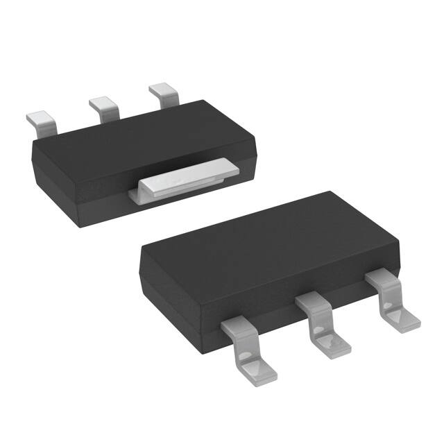
DCY (SOT-223) PACKAGE
(TOP VIEW)
COMMON
KTP PACKAGE
(TOP VIEW)
OUTPUT
COMMON
OUTPUT
COMMON
INPUT
COMMON
INPUT
description/ordering information
This series of fixed-voltage integrated-circuit voltage regulators is designed for a wide range of applications.
These applications include on-card regulation for elimination of noise and distribution problems associated with
single-point regulation. Each of these regulators can deliver up to 500 mA of output current. The internal
current-limiting and thermal-shutdown features of these regulators essentially make them immune to overload.
In addition to use as fixed-voltage regulators, these devices can be used with external components to obtain
adjustable output voltages and currents and also as the power-pass element in precision regulators.
ORDERING INFORMATION{
TJ
VO(NOM)
(V)
33
3.3
−40°C
40 C to 125
125°C
C
5
8
10
ORDERABLE
PART NUMBER
PACKAGE‡
TOP-SIDE
MARKING
PowerFLEX (KTP)
Reel of 3000
UA78M33QKTPRQ1
78M33CQ
SOT-223 (DCY)
Reel of 2500
UA78M33QDCYRQ1
C3Q
PowerFLEX (KTP)
Reel of 3000
UA78M05QKTPRQ1
78M05CQ
SOT-223 (DCY)
Reel of 2500
UA78M05QDCYRQ1
C5Q
PowerFLEX (KTP)
Reel of 3000
UA78M08QKTPRQ1
78M08CQ
SOT-223 (DCY)
Reel of 2500
UA78M08QDCYRQ1
C8Q
PowerFLEX (KTP)
Reel of 3000
UA78M10QKTPRQ1
78M10CQ
†
For the most current package and ordering information, see the Package Option Addendum at the end of this document, or see
the TI web site at www.ti.com.
‡ Package drawings, thermal data, and symbolization are available at www.ti.com/packaging.
Please be aware that an important notice concerning availability, standard warranty, and use in critical applications of
Texas Instruments semiconductor products and disclaimers thereto appears at the end of this data sheet.
PowerFLEX is a trademark of Texas Instruments.
Copyright 2008, Texas Instruments Incorporated
PRODUCTION DATA information is current as of publication date.
Products conform to specifications per the terms of Texas Instruments
standard warranty. Production processing does not necessarily include
testing of all parameters.
POST OFFICE BOX 655303
• DALLAS, TEXAS 75265
1
�uA78Mxx-Q1 SERIES
POSITIVE-VOLTAGE REGULATORS
SLVS537B − JUNE 2004 − REVISED SEPTEMBER 2008
schematic
INPUT
140 kΩ
96 Ω
0.6 Ω
OUTPUT
0 to 20 kΩ
5.4 kΩ
COMMON
Resistor values shown are nominal.
2
POST OFFICE BOX 655303
• DALLAS, TEXAS 75265
�uA78Mxx-Q1 SERIES
POSITIVE-VOLTAGE REGULATORS
SLVS537B − JUNE 2004 − REVISED SEPTEMBER 2008
absolute maximum ratings over virtual junction temperature range (unless otherwise noted)†
Input voltage, VI . . . . . . . . . . . . . . . . . . . . . . . . . . . . . . . . . . . . . . . . . . . . . . . . . . . . . . . . . . . . . . . . . . . . . . . . . . . 35 V
Operating virtual junction temperature, TJ . . . . . . . . . . . . . . . . . . . . . . . . . . . . . . . . . . . . . . . . . . . . . . . . . . . 150°C
Lead temperature 1,6 mm (1/16 inch) from case for 10 seconds
. . . . . . . . . . . . . . . . . . . . . . . . . . . . . . 260°C
Storage temperature range, Tstg . . . . . . . . . . . . . . . . . . . . . . . . . . . . . . . . . . . . . . . . . . . . . . . . . . −65°C to 150°C
†
Stresses beyond those listed under “absolute maximum ratings” may cause permanent damage to the device. These are stress ratings only, and
functional operation of the device at these or any other conditions beyond those indicated under “recommended operating conditions” is not
implied. Exposure to absolute-maximum-rated conditions for extended periods may affect device reliability.
package thermal data (see Note 1)
PACKAGE
BOARD
θJC
θJA
PowerFLEX (KTP)
High K, JESD 51-5
19°C/W
28°C/W
SOT-223 (DCY)
High K, JESD 51-7
4°C/W
53°C/W
NOTE 1: Maximum power dissipation is a function of TJ(max), θJA, and TA. The maximum allowable power dissipation at any allowable ambient
temperature is PD = (TJ(max) − TA)/θJA. Operating at the absolute maximum TJ of 150°C can affect reliability.
recommended operating conditions
VI
Input voltage
IO
Output current
TJ
Operating virtual junction temperature
POST OFFICE BOX 655303
MIN
MAX
µA78M33
5.3
25
µA78M05
7
25
µA78M06
8
25
µA78M08
10.5
25
µA78M09
11.5
26
µA78M10
12.5
28
µA78M12
14.5
−40
• DALLAS, TEXAS 75265
UNIT
V
30
500
mA
125
°C
3
�uA78Mxx-Q1 SERIES
POSITIVE-VOLTAGE REGULATORS
SLVS537B − JUNE 2004 − REVISED SEPTEMBER 2008
electrical characteristics at specified virtual junction temperature, VI = 8 V, IO = 350 mA, TJ = 25°C
(unless otherwise noted)
TEST CONDITIONS†
PARAMETER
µA78M33Q
MIN
TYP
MAX
3.2
3.3
3.4
3.1
3.3
3.5
VI = 5.3 V to 25 V
9
100
VI = 8 V to 25 V
3
50
‡
O t t voltage
Output
lt
IO = 5 mA to 350 mA,
VI = 8 V to 20 V
Input voltage regulation
IO = 200 mA
VI = 8 V to 18 V,
f = 120 Hz
IO = 100 mA, TJ = −40°C to 125°C
62
Ripple rejection
IO = 300 mA
62
Output voltage regulation
VI = 8 V,
IO = 5 mA to 500 mA
20
Temperature coefficient of output voltage
IO = 5 mA,
TJ = −40°C to 125°C
−1
Output noise voltage
f = 10 Hz to 100 kHz
TJ = −40°C to 125°C
Dropout voltage
4.5
Bias current change
Short-circuit output current
100
µV
6
mA
V
VI = 8 V to 25 V,
0.8
IO = 5 mA to 350 mA,
TJ = −40°C to 125°C
0.5
VI = 35 V
mV
200
IO = 200 mA,
TJ = −40°C to 125°C
Peak output current
mV
mV/°C
2
Bias current
V
dB
80
40
UNIT
mA
300
mA
700
mA
†
All characteristics are measured with a 0.33-µF capacitor across the input and a 0.1-µF capacitor across the output. Pulse-testing techniques
maintain TJ as close to TA as possible. Thermal effects must be taken into account separately.
‡ This specification applies only for dc power dissipation permitted by absolute maximum ratings.
electrical characteristics at specified virtual junction temperature, VI = 10 V, IO = 350 mA, TJ = 25°C
(unless otherwise noted)
TEST CONDITIONS†
PARAMETER
O tp t voltage
oltage
Output
IO = 5 mA to 350 mA,
VI = 7 V to 20 V
Input voltage regulation
IO = 200 mA
Ripple rejection
VI = 8 V to 18 V,
f = 120 Hz
Output voltage regulation
TJ = −40°C to 125°C
5
5.2
4.75
5.25
3
100
VI = 8 V to 25 V
1
50
IO = 100 mA, TJ = −40°C to 125°C
62
IO = 300 mA
62
100
10
50
Output noise voltage
f = 10 Hz to 100 kHz
TJ = −40°C to 125°C
−1
40
mV
µV
6
mA
V
VI = 8 V to 25 V,
0.8
IO = 5 mA to 350 mA,
TJ = −40°C to 125°C
0.5
Peak output current
mV
200
IO = 200 mA,
TJ = −40°C to 125°C
VI = 35 V
V
mV/°C
2
4.5
UNIT
dB
80
20
Bias current
4
4.8
VI = 7 V to 25 V
Dropout voltage
†
MAX
IO = 5 mA to 200 mA
IO = 5 mA,
Short-circuit output current
TYP
IO = 5 mA to 500 mA
Temperature coefficient of output voltage
Bias current change
µA78M05Q
MIN
mA
300
mA
0.7
A
All characteristics are measured with a 0.33-µF capacitor across the input and a 0.1-µF capacitor across the output. Pulse-testing techniques
maintain TJ as close to TA as possible. Thermal effects must be taken into account separately.
POST OFFICE BOX 655303
• DALLAS, TEXAS 75265
�uA78Mxx-Q1 SERIES
POSITIVE-VOLTAGE REGULATORS
SLVS537B − JUNE 2004 − REVISED SEPTEMBER 2008
electrical characteristics at specified virtual junction temperature, VI = 14 V, IO = 350 mA, TJ = 25°C
(unless otherwise noted)
O t t voltage
Output
lt
VI = 10.5
10 5 V to 23 V,
V
Input voltage regulation
IO = 200 mA
Ripple rejection
VI = 11.5 V to 21.5 V,
f = 120 Hz
Output voltage regulation
µA78M08Q
TEST CONDITIONS†
PARAMETER
IO = 5 mA to 350 mA
TJ = −40°C to 125°C
MIN
TYP
MAX
7.7
8
8.3
7.6
VI = 10.5 V to 25 V
6
100
VI = 11 V to 25 V
2
50
IO = 100 mA,
TJ = −40°C to 125°C
IO = 300 mA
56
25
160
10
80
Output noise voltage
f = 10 Hz to 100 kHz
TJ = −40°C to 125°C
Dropout voltage
Short-circuit output current
IO = 200 mA,
TJ = −40°C to 125°C
52
µV
TJ = −40°C to 125°C
V
6
mA
0.8
0.5
VI = 35 V
Peak output current
†
mV/°C
4.6
IO = 5 mA to 350 mA,
mV
−1
2
Bias current
VI = 10.5 V to 25 V,
mV
dB
80
IO = 5 mA to 200 mA
IO = 5 mA,
V
56
IO = 5 mA to 500 mA
Temperature coefficient
of output voltage
Bias current change
8.4
UNIT
mA
250
mA
0.7
A
All characteristics are measured with a 0.33-µF capacitor across the input and a 0.1-µF capacitor across the output. Pulse-testing techniques
maintain TJ as close to TA as possible. Thermal effects must be taken into account separately.
electrical characteristics at specified virtual junction temperature, VI = 17 V, IO = 350 mA, TJ = 25°C
(unless otherwise noted)
O t t voltage
Output
lt
VI = 12.5
12 5 V to 25 V,
V
Input voltage regulation
IO = 200 mA
Ripple rejection
VI = 15 V to 25 V,
f = 120 Hz
Output voltage regulation
µA78M10Q
TEST CONDITIONS†
PARAMETER
IO = 5 mA to 350 mA
TJ = −40°C to 125°C
9.6
10
10.4
9.5
10.5
VI = 12.5 V to 28 V
7
100
VI = 14 V to 28 V
2
50
IO = 100 mA,
TJ = −40°C to 125°C
IO = 300 mA
IO = 5 mA to 200 mA
10
100
Output noise voltage
f = 10 Hz to 100 kHz
IO = 200 mA,
IO = 5 mA to 350 mA,
TJ = −40°C to 125°C
64
µV
TJ = −40°C to 125°C
VI = 35 V
Peak output current
mV
mV/°C
4.7
VI = 12.5 V to 28 V,
mV
−1
2
Bias current
V
dB
80
200
TJ = −40°C to 125°C
UNIT
59
55
Dropout voltage
†
MAX
25
IO = 5 mA,
Short-circuit output current
TYP
IO = 5 mA to 500 mA
Temperature coefficient
of output voltage
Bias current change
MIN
V
6
mA
0.8
0.5
mA
245
mA
0.7
A
All characteristics are measured with a 0.33-µF capacitor across the input and a 0.1-µF capacitor across the output. Pulse-testing techniques
maintain TJ as close to TA as possible. Thermal effects must be taken into account separately.
POST OFFICE BOX 655303
• DALLAS, TEXAS 75265
5
�PACKAGE OPTION ADDENDUM
www.ti.com
6-Feb-2020
PACKAGING INFORMATION
Orderable Device
Status
(1)
Package Type Package Pins Package
Drawing
Qty
Eco Plan
Lead/Ball Finish
MSL Peak Temp
(2)
(6)
(3)
Op Temp (°C)
Device Marking
(4/5)
UA78M05QDCYRG4Q1
ACTIVE
SOT-223
DCY
4
2500
Green (RoHS
& no Sb/Br)
NIPDAU
Level-2-260C-1 YEAR
-40 to 125
C5Q
UA78M05QDCYRQ1
ACTIVE
SOT-223
DCY
4
2500
Green (RoHS
& no Sb/Br)
NIPDAU
Level-2-260C-1 YEAR
-40 to 125
C5Q
UA78M33QDCYRG4Q1
ACTIVE
SOT-223
DCY
4
2500
Green (RoHS
& no Sb/Br)
NIPDAU
Level-2-260C-1 YEAR
-40 to 125
C3Q
(1)
The marketing status values are defined as follows:
ACTIVE: Product device recommended for new designs.
LIFEBUY: TI has announced that the device will be discontinued, and a lifetime-buy period is in effect.
NRND: Not recommended for new designs. Device is in production to support existing customers, but TI does not recommend using this part in a new design.
PREVIEW: Device has been announced but is not in production. Samples may or may not be available.
OBSOLETE: TI has discontinued the production of the device.
(2)
RoHS: TI defines "RoHS" to mean semiconductor products that are compliant with the current EU RoHS requirements for all 10 RoHS substances, including the requirement that RoHS substance
do not exceed 0.1% by weight in homogeneous materials. Where designed to be soldered at high temperatures, "RoHS" products are suitable for use in specified lead-free processes. TI may
reference these types of products as "Pb-Free".
RoHS Exempt: TI defines "RoHS Exempt" to mean products that contain lead but are compliant with EU RoHS pursuant to a specific EU RoHS exemption.
Green: TI defines "Green" to mean the content of Chlorine (Cl) and Bromine (Br) based flame retardants meet JS709B low halogen requirements of


 工商网监
湘ICP备2023018690号
工商网监
湘ICP备2023018690号
