Product
Folder
Sample &
Buy
Support &
Community
Tools &
Software
Technical
Documents
uA78M05, uA78M06, uA78M08
uA78M09, uA78M10, uA78M12, uA78M33
SLVS059T – JUNE 1976 – REVISED JANUARY 2015
µA78Mxx Positive-Voltage Regulators
1 Features
3 Description
•
•
•
•
•
•
•
This series of fixed-voltage integrated-circuit voltage
regulators is designed for a wide range of
applications. The applications include on-card
regulation for elimination of noise and distribution
problems associated with single-point regulation.
Each of these regulators can deliver up to 500 mA of
output current. The internal current-limiting and
thermal-shutdown features of these regulators
essentially make them immune to overload. In
addition to use as fixed-voltage regulators, these
devices can be used with external components to
obtain adjustable output voltages and currents and
also as the power-pass element in precision
regulators.
1
3-Terminal Regulators
Output Current up to 500 mA
No External Components
Internal Thermal-Overload Protection
High Power-Dissipation Capability
Internal Short-Circuit Current Limiting
Output Transistor Safe-Area Compensation
2 Applications
•
•
•
•
On-Card Regulation
Portable Devices
Computing & Servers
Telecommunications
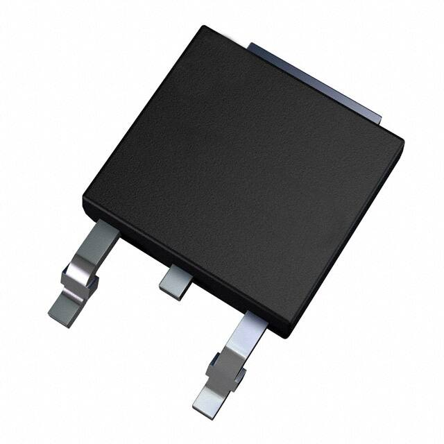
Device Information(1)
PART NUMBER
UA78Mxx
PACKAGE
BODY SIZE (NOM)
SOT-223 (3)
6.50 mm x 3.50 mm
TO-220 (3)
10.16 mm x 8.82 mm
TO-252 (3)
6.60 mm x 6.10 mm
(1) For all available packages, see the orderable addendum at
the end of the data sheet.
4 Simplified Schematic
INPUT
Unregulated Voltage Source
OUTPUT
Up to 500 mA
UA78MXX
0.33 PF
COMMON
0.1 PF
1
An IMPORTANT NOTICE at the end of this data sheet addresses availability, warranty, changes, use in safety-critical applications,
intellectual property matters and other important disclaimers. PRODUCTION DATA.
�uA78M05, uA78M06, uA78M08
uA78M09, uA78M10, uA78M12, uA78M33
SLVS059T – JUNE 1976 – REVISED JANUARY 2015
www.ti.com
Table of Contents
1
2
3
4
5
6
7
Features ..................................................................
Applications ...........................................................
Description .............................................................
Simplified Schematic.............................................
Revision History.....................................................
Pin Configuration and Functions .........................
Specifications.........................................................
1
1
1
1
2
3
4
7.1
7.2
7.3
7.4
7.5
7.6
7.7
7.8
7.9
7.10
7.11
7.12
7.13
4
4
4
4
5
5
6
6
7
7
8
8
9
Absolute Maximum Ratings ......................................
ESD Ratings ............................................................
Recommended Operating Conditions.......................
Thermal Information ..................................................
Electrical Characteristics — uA78M33C ...................
Electrical Characteristics — uA78M33I.....................
Electrical Characteristics — uA78M05C ...................
Electrical Characteristics — uA78M05I.....................
Electrical Characteristics — uA78M06C ...................
Electrical Characteristics — uA78M08C .................
Electrical Characteristics — uA78M09C .................
Electrical Characteristics — uA78M10C .................
Electrical Characteristics — uA78M12C .................
7.14 Typical Characteristics ............................................ 9
8
Detailed Description ............................................ 10
8.1
8.2
8.3
8.4
9
Overview .................................................................
Functional Block Diagram .......................................
Feature Description.................................................
Device Functional Modes........................................
10
10
10
10
Application and Implementation ........................ 11
9.1 Application Information............................................ 11
9.2 Typical Application ................................................. 11
10 Power Supply Recommendations ..................... 13
11 Layout................................................................... 13
11.1 Layout Guidelines ................................................. 13
11.2 Layout Example .................................................... 13
12 Device and Documentation Support ................. 14
12.1
12.2
12.3
12.4
Related Links ........................................................
Trademarks ...........................................................
Electrostatic Discharge Caution ............................
Glossary ................................................................
14
14
14
14
13 Mechanical, Packaging, and Orderable
Information ........................................................... 14
5 Revision History
Changes from Revision S (May 2013) to Revision T
•
Page
Added Applications, Device Information table, Pin Functions table, ESD Ratings table, Thermal Information table,
Typical Characteristics, Feature Description section, Device Functional Modes, Application and Implementation
section, Power Supply Recommendations section, Layout section, Device and Documentation Support section, and
Mechanical, Packaging, and Orderable Information section. ................................................................................................. 1
Changes from Revision R (February 2013) to Revision S
•
Page
Removed Ordering Information table. .................................................................................................................................... 1
Changes from Revision Q (April 2010) to Revision R
•
2
Page
Removed obsolete part information from document. ............................................................................................................. 1
Submit Documentation Feedback
Copyright © 1976–2015, Texas Instruments Incorporated
Product Folder Links: uA78M05 uA78M06 uA78M08 uA78M09 uA78M10 uA78M12 uA78M33
�uA78M05, uA78M06, uA78M08
uA78M09, uA78M10, uA78M12, uA78M33
www.ti.com
SLVS059T – JUNE 1976 – REVISED JANUARY 2015
6 Pin Configuration and Functions
COMMON
KC (TO-220) PACKAGE
(TOP VIEW)
KTP (PowerFLEX /TO-252*) PACKAGE
(TOP VIEW)
COMMON
OUTPUT
COMMON
INPUT
COMMON
KCS (TO-220) PACKAGE
(TOP VIEW)
OUTPUT
COMMON
INPUT
* Complies with JEDEC TO-252, variation AC
OUTPUT
COMMON
INPUT
DCY (SOT-223) PACKAGE
(TOP VIEW)
COMMON
OUTPUT
COMMON
KVU (TO-252) PACKAGE
(TOP VIEW)
OUTPUT
COMMON
INPUT
COMMON
INPUT
Pin Functions
PIN
NAME
NO.
TYPE
COMMON
2
INPUT
1
I
Supply Input
OUTPUT
3
O
Voltage Output
Copyright © 1976–2015, Texas Instruments Incorporated
—
DESCRIPTION
Ground
Submit Documentation Feedback
Product Folder Links: uA78M05 uA78M06 uA78M08 uA78M09 uA78M10 uA78M12 uA78M33
3
�uA78M05, uA78M06, uA78M08
uA78M09, uA78M10, uA78M12, uA78M33
SLVS059T – JUNE 1976 – REVISED JANUARY 2015
www.ti.com
7 Specifications
7.1 Absolute Maximum Ratings
over virtual junction temperature range (unless otherwise noted)
(1)
MIN
VI
Input voltage
TJ
Operating virtual junction temperature
Tstg
Storage temperature range
(1)
MAX
–65
UNIT
35
V
150
°C
150
°C
Stresses beyond those listed under Absolute Maximum Ratings may cause permanent damage to the device. These are stress ratings
only, and functional operation of the device at these or any other conditions beyond those indicated under Recommended Operating
Conditions is not implied. Exposure to absolute-maximum-rated conditions for extended periods may affect device reliability.
7.2 ESD Ratings
VALUE
V(ESD)
(1)
(2)
Electrostatic discharge
Human body model (HBM), per ANSI/ESDA/JEDEC JS-001, all pins (1)
2500
Charged device model (CDM), per JEDEC specification JESD22-C101,
all pins (2)
2000
UNIT
V
JEDEC document JEP155 states that 500-V HBM allows safe manufacturing with a standard ESD control process.
JEDEC document JEP157 states that 250-V CDM allows safe manufacturing with a standard ESD control process.
7.3 Recommended Operating Conditions
VI
Input voltage
IO
MIN
MAX
uA78M33
5.3
25
uA78M05
7
25
uA78M06
8
25
uA78M08
10.5
25
uA78M09
11.5
26
uA78M10
12.5
28
uA78M12
14.5
30
uA78M15
17.5
30
Output current
TJ
500
uA78MxxC
Operating virtual junction temperature
uA78MxxI
0
125
–40
125
UNIT
V
mA
°C
7.4 Thermal Information
UA78Mxx
THERMAL METRIC
(1)
RθJA
Junction-to-ambient thermal resistance
RθJC(to
Junction-to-case (top) thermal resistance
DCY
KC
KCS
KTP
KVU
3 PINS
3 PINS
3 PINS
3 PINS
3 PINS
53
19
19
28
30.3
30.6
17
17
19
—
—
3
3
1.4
—
p)
RθJC(b
Junction-to-case (bottom) thermal resistance
UNIT
°C/W
ot)
(1)
4
For more information about traditional and new thermal metrics, see the IC Package Thermal Metrics application report, SPRA953.
Submit Documentation Feedback
Copyright © 1976–2015, Texas Instruments Incorporated
Product Folder Links: uA78M05 uA78M06 uA78M08 uA78M09 uA78M10 uA78M12 uA78M33
�uA78M05, uA78M06, uA78M08
uA78M09, uA78M10, uA78M12, uA78M33
www.ti.com
SLVS059T – JUNE 1976 – REVISED JANUARY 2015
7.5 Electrical Characteristics — uA78M33C
at specified virtual junction temperature, VI = 8 V, IO = 350 mA, TJ = 25°C (unless otherwise noted)
uA78M33C
TEST CONDITIONS (1)
PARAMETER0
MIN
TYP MAX
3.2
3.3
3.4
3.1
3.3
3.5
VI = 5.3 V to 25 V
9
100
VI = 8 V to 25 V
3
50
Output voltage (2)
IO = 5 mA to 350 mA,
VI = 8 V to 20 V
Input voltage regulation
IO = 200 mA
Ripple rejection
VI = 8 V to 18 V,
f = 120 Hz
IO = 100 mA, TJ = 0°C to 125°C
62
IO = 300 mA
62
Output voltage regulation
VI = 8 V,
IO = 5 mA to 500 mA
20
Temperature coefficient
of output voltage
IO = 5 mA,
TJ = 0°C to 125°C
–1
Output noise voltage
f = 10 Hz to 100 kHz
TJ = 0°C to 125°C
4.5
IO = 200 mA,
Bias current change
VI = 8 V to 25 V,
IO = 5 mA to 350 mA,
Short-circuit output
current
dB
100
mV
mV/°C
200
μV
6
mA
V
TJ = 0°C to 125°C
0.8
TJ = 0°C to 125°C
0.5
VI = 35 V
Peak output current
(2)
mV
2
Bias current
(1)
V
80
40
Dropout voltage
UNIT
mA
300
mA
700
mA
All characteristics are measured with a 0.33-μF capacitor across the input and a 0.1-μF capacitor across the output. Pulse-testing
techniques maintain TJ as close to TA as possible. Thermal effects must be taken into account separately.
This specification applies only for dc power dissipation permitted by Absolute Maximum Ratings.
7.6 Electrical Characteristics — uA78M33I
at specified virtual junction temperature, VI = 8 V, IO = 350 mA, TJ = 25°C (unless otherwise noted)
uA78M33I
TEST CONDITIONS (1)
PARAMETER
Output voltage (2)
IO = 5 mA to 350 mA,
VI = 8 V to 20 V
Input voltage regulation
IO = 200 mA
Ripple rejection
VI = 8 V to 18 V,
f = 120 Hz
MIN
TYP MAX
3.2
3.3
3.4
3.1
3.3
3.5
VI = 5.3 V to 25 V
9
100
VI = 8 V to 25 V
3
50
TJ = –40°C to 125°C
IO = 100 mA, TJ = –40°C to
125°C
62
IO = 300 mA
62
IO = 5 mA to 500 mA
20
Temperature coefficient
of output voltage
IO = 5 mA,
TJ = –40°C to 125°C
–1
Output noise voltage
f = 10 Hz to 100 kHz
40
4.5
IO = 200 mA,
IO = 5 mA to 350 mA,
VI = 8 V to 25 V,
(2)
mV
mV/°C
200
μV
6
mA
V
TJ = –40°C to 125°C
0.8
TJ = –40°C to 125°C
0.5
VI = 35 V
Peak output current
(1)
100
2
Bias current
Short-circuit output
current
mV
dB
VI = 8 V,
Bias current change
V
80
Output voltage regulation
Dropout voltage
UNIT
mA
300
mA
700
mA
All characteristics are measured with a 0.33-μF capacitor across the input and a 0.1-μF capacitor across the output. Pulse-testing
techniques maintain TJ as close to TA as possible. Thermal effects must be taken into account separately.
This specification applies only for dc power dissipation permitted by Absolute Maximum Ratings.
Copyright © 1976–2015, Texas Instruments Incorporated
Submit Documentation Feedback
Product Folder Links: uA78M05 uA78M06 uA78M08 uA78M09 uA78M10 uA78M12 uA78M33
5
�uA78M05, uA78M06, uA78M08
uA78M09, uA78M10, uA78M12, uA78M33
SLVS059T – JUNE 1976 – REVISED JANUARY 2015
www.ti.com
7.7 Electrical Characteristics — uA78M05C
at specified virtual junction temperature, VI = 10 V, IO = 350 mA, TJ = 25°C (unless otherwise noted)
Output voltage (2)
IO = 5 mA to 350 mA,
VI = 7 V to 20 V
Input voltage regulation
IO = 200 mA
Ripple rejection
VI = 8 V to 18 V,
f = 120 Hz
Output voltage regulation
uA78M05C
TEST CONDITIONS (1)
PARAMETER
TJ = 0°C to 125°C
MIN
TYP
4.8
5
VI = 7 V to 25 V
3
100
VI = 8 V to 25 V
1
50
62
IO = 300 mA
62
100
10
50
f = 10 Hz to 100 kHz
TJ = 0°C to 125°C
mV
–1
mV/°C
40
Dropout voltage
200
μV
6
mA
2
Bias current
V
4.5
Bias current change
Short-circuit output current
IO = 200 mA, VI = 8 V to 25 V, TJ = 0°C to 125°C
0.8
IO = 5 mA to 350 mA,
0.5
TJ = 0°C to 125°C
VI = 35 V
Peak output current
(2)
dB
20
Output noise voltage
mV
80
IO = 5 mA to 200 mA
IO = 5 mA,
V
5.25
IO = 5 mA to 500 mA
Temperature coefficient
of output voltage
(1)
5.2
4.75
IO = 100 mA, TJ = 0°C to 125°C
UNIT
MAX
mA
300
mA
0.7
A
All characteristics are measured with a 0.33-μF capacitor across the input and a 0.1-μF capacitor across the output. Pulse-testing
techniques maintain TJ as close to TA as possible. Thermal effects must be taken into account separately.
This specification applies only for dc power dissipation permitted by Absolute Maximum Ratings.
7.8 Electrical Characteristics — uA78M05I
at specified virtual junction temperature, VI = 10 V, IO = 350 mA, TJ = 25°C (unless otherwise noted)
uA78M05I
TEST CONDITIONS (1)
PARAMETER
Output voltage (2)
IO = 5 mA to 350 mA,
VI = 7 V to 20 V
Input voltage regulation
IO = 200 mA
Ripple rejection
VI = 8 V to 18 V,
f = 120 Hz
Output voltage
regulation
MIN
4.8
TJ = –40°C to 125°C
4.75
3
100
VI = 8 V to 25 V
1
50
62
IO = 300 mA
62
10
50
f = 10 Hz to 100 kHz
4.5
IO = 200 mA,
VI = 8 V to 25 V,
mV/°C
200
μV
6
mA
IO = 5 mA to 350 mA,
V
TJ = –40°C to 125°C
0.8
TJ = –40°C to 125°C
0.5
VI = 35 V
Peak output current
6
mV
2
Bias current
(2)
–1
40
Dropout voltage
(1)
dB
IO = 5 mA to 200 mA
Output noise voltage
mV
80
100
TJ = –40°C to 125°C
V
5.25
VI = 7 V to 25 V
IO = 100 mA, TJ = –40°C to 125°C
UNIT
5.2
20
IO = 5 mA,
Short-circuit output
current
5
IO = 5 mA to 500 mA
Temperature coefficient
of output voltage
Bias current change
TYP MAX
mA
300
mA
0.7
A
All characteristics are measured with a 0.33-μF capacitor across the input and a 0.1-μF capacitor across the output. Pulse-testing
techniques maintain TJ as close to TA as possible. Thermal effects must be taken into account separately.
This specification applies only for dc power dissipation permitted by Absolute Maximum Ratings.
Submit Documentation Feedback
Copyright © 1976–2015, Texas Instruments Incorporated
Product Folder Links: uA78M05 uA78M06 uA78M08 uA78M09 uA78M10 uA78M12 uA78M33
�uA78M05, uA78M06, uA78M08
uA78M09, uA78M10, uA78M12, uA78M33
www.ti.com
SLVS059T – JUNE 1976 – REVISED JANUARY 2015
7.9 Electrical Characteristics — uA78M06C
at specified virtual junction temperature, VI = 11 V, IO = 350 mA, TJ = 25°C (unless otherwise noted)
uA78M06C
TEST CONDITIONS (1)
PARAMETER
Output voltage (2)
IO = 5 mA to 350 mA,
Input voltage regulation
IO = 200 mA
Ripple rejection
VI = 8 V to 18 V,
Output voltage regulation
VI = 8 V to 21 V
MIN
5.75
TJ = 0°C to 125°C
5
100
VI = 9 V to 25 V
1.5
50
IO = 100 mA,
TJ = 0°C to 125°C
59
IO = 300 mA
59
dB
120
10
60
Output noise voltage
f = 10 Hz to 100 kHz
Dropout voltage
Bias current
Bias current change
Short-circuit output current
IO = 200 mA,
IO = 5 mA to 350 mA,
TJ = 0°C to 125°C
mV
–1
mV/°C
45
μV
2
V
4.5
VI = 9 V to 25 V,
mV
80
20
TJ = 0°C to 125°C
V
6.3
VI = 8 V to 25 V
f = 120 Hz
UNIT
6.25
IO = 5 mA to 200 mA
IO = 5 mA,
TJ = 0°C to 125°C
6
mA
0.8
mA
0.5
VI = 35 V
Peak output current
(2)
6
5.7
IO = 5 mA to 500 mA
Temperature coefficient
of output voltage
(1)
TYP MAX
270
mA
0.7
A
All characteristics are measured with a 0.33-μF capacitor across the input and a 0.1-μF capacitor across the output. Pulse-testing
techniques maintain TJ as close to TA as possible. Thermal effects must be taken into account separately.
This specification applies only for dc power dissipation permitted by Absolute Maximum Ratings.
7.10 Electrical Characteristics — uA78M08C
at specified virtual junction temperature, VI = 14 V, IO = 350 mA, TJ = 25°C (unless otherwise noted)
uA78M08C
TEST CONDITIONS (1)
PARAMETER
Output voltage (2)
VI = 10.5 V to 23 V,
Input voltage regulation
IO = 200 mA
Ripple rejection
VI = 11 V to 21.5 V,
f = 120 Hz
Output voltage regulation
IO = 5 mA to 350 mA
MIN
7.7
TJ = 0°C to 125°C
6
100
VI = 11 V to 25 V
2
50
TJ = 0°C to 125°C
IO = 300 mA
56
160
80
TJ = 0°C to 125°C
Dropout voltage
–1
mV/°C
52
μV
4.6
VI = 10.5 V to 25 V,
IO = 200 mA,
IO = 5 mA to 350 mA,
TJ = 0°C to 125°C
TJ = 0°C to 125°C
V
6
0.8
0.5
VI = 35 V
Peak output current
(2)
mV
2
Bias current
(1)
dB
80
10
f = 10 Hz to 100 kHz
mV
56
25
Output noise voltage
V
8.4
VI = 10.5 V to 25 V
IO = 100 mA,
UNIT
8.3
IO = 5 mA to 200 mA
IO = 5 mA,
Short-circuit output
current
8
7.6
IO = 5 mA to 500 mA
Temperature coefficient
of output voltage
Bias current change
TYP MAX
mA
mA
250
mA
0.7
A
All characteristics are measured with a 0.33-μF capacitor across the input and a 0.1-μF capacitor across the output. Pulse-testing
techniques maintain TJ as close to TA as possible. Thermal effects must be taken into account separately.
This specification applies only for dc power dissipation permitted by Absolute Maximum Ratings.
Copyright © 1976–2015, Texas Instruments Incorporated
Submit Documentation Feedback
Product Folder Links: uA78M05 uA78M06 uA78M08 uA78M09 uA78M10 uA78M12 uA78M33
7
�uA78M05, uA78M06, uA78M08
uA78M09, uA78M10, uA78M12, uA78M33
SLVS059T – JUNE 1976 – REVISED JANUARY 2015
www.ti.com
7.11 Electrical Characteristics — uA78M09C
at specified virtual junction temperature, VI = 16 V, IO = 350 mA, TJ = 25°C (unless otherwise noted)
uA78M09C
TEST CONDITIONS (1)
PARAMETER
Output voltage (2)
VI = 11.5 V to 24 V,
Input voltage regulation
IO = 200 mA
Ripple rejection
VI = 13 V to 23 V,
f = 120 Hz
Output voltage regulation
IO = 5 mA to 350 mA
MIN
8.6
TJ = 0°C to 125°C
6
100
VI = 12 V to 26 V
2
50
TJ = 0°C to 125°C
IO = 300 mA
56
dB
80
180
10
90
f = 10 Hz to 100 kHz
mV
56
25
Output noise voltage
V
9.5
VI = 11.5 V to 26 V
IO = 100 mA,
UNIT
9.4
IO = 5 mA to 200 mA
IO = 5 mA,
TJ = 0°C to 125°C
Dropout voltage
mV
–1
mV/°C
58
μV
2
Bias current
V
4.6
Bias current change
Short-circuit output
current
VI = 11.5 V to 26 V,
IO = 200 mA,
IO = 5 mA to 350 mA,
TJ = 0°C to 125°C
6
TJ = 0°C to 125°C
mA
0.8
mA
0.5
VI = 35 V
Peak output current
(2)
9
8.5
IO = 5 mA to 500 mA
Temperature coefficient
of output voltage
(1)
TYP MAX
250
mA
0.7
A
All characteristics are measured with a 0.33-μF capacitor across the input and a 0.1-μF capacitor across the output. Pulse-testing
techniques maintain TJ as close to TA as possible. Thermal effects must be taken into account separately.
This specification applies only for dc power dissipation permitted by Absolute Maximum Ratings.
7.12 Electrical Characteristics — uA78M10C
at specified virtual junction temperature, VI = 17 V, IO = 350 mA, TJ = 25°C (unless otherwise noted)
uA78M10C
TEST CONDITIONS (1)
PARAMETER
Output voltage (2)
VI = 12.5 V to 25 V,
Input voltage regulation
IO = 200 mA
Ripple rejection
VI = 15 V to 25 V,
f = 120 Hz
Output voltage regulation
IO = 5 mA to 350 mA
MIN
9.6
TJ = 0°C to 125°C
7
100
VI = 14 V to 28 V
2
50
TJ = 0°C to 125°C
IO = 300 mA
55
200
100
TJ = 0°C to 125°C
Dropout voltage
8
–1
mV/°C
64
μV
4.7
VI = 12.5 V to 28 V,
IO = 200 mA,
IO = 5 mA to 350 mA,
TJ = 0°C to 125°C
TJ = 0°C to 125°C
V
6
0.8
0.5
VI = 35 V
Peak output current
(2)
mV
2
Bias current
(1)
dB
80
10
f = 10 Hz to 100 kHz
mV
59
25
Output noise voltage
V
10.5
VI = 12.5 V to 28 V
IO = 100 mA,
UNIT
10.4
IO = 5 mA to 200 mA
IO = 5 mA,
Short-circuit output
current
10
9.5
IO = 5 mA to 500 mA
Temperature coefficient
of output voltage
Bias current change
TYP MAX
mA
mA
245
mA
0.7
A
All characteristics are measured with a 0.33-μF capacitor across the input and a 0.1-μF capacitor across the output. Pulse-testing
techniques maintain TJ as close to TA as possible. Thermal effects must be taken into account separately.
This specification applies only for dc power dissipation permitted by Absolute Maximum Ratings.
Submit Documentation Feedback
Copyright © 1976–2015, Texas Instruments Incorporated
Product Folder Links: uA78M05 uA78M06 uA78M08 uA78M09 uA78M10 uA78M12 uA78M33
�uA78M05, uA78M06, uA78M08
uA78M09, uA78M10, uA78M12, uA78M33
www.ti.com
SLVS059T – JUNE 1976 – REVISED JANUARY 2015
7.13 Electrical Characteristics — uA78M12C
at specified virtual junction temperature, VI = 19 V, IO = 350 mA, TJ = 25°C (unless otherwise noted)
uA78M12C
TEST CONDITIONS (1)
PARAMETER
Output voltage (2)
VI = 14.5 V to 27 V,
Input voltage regulation
IO = 200 mA
Ripple rejection
VI = 15 V to 25 V,
f = 120 Hz
Output voltage regulation
MIN
11.5
IO = 5 mA to 350 mA
TJ = 0°C to 125°C
8
100
VI = 16 V to 30 V
2
50
TJ = 0°C to 125°C
IO = 300 mA
55
240
120
TJ = 0°C to 125°C
Dropout voltage
–1
mV/°C
75
μV
4.8
VI = 14.5 V to 30 V,
IO = 200 mA,
IO = 5 mA to 350 mA,
TJ = 0°C to 125°C
TJ = 0°C to 125°C
V
6
0.8
0.5
VI = 35 V
Peak output current
(2)
mV
2
Bias current
(1)
dB
80
10
f = 10 Hz to 100 kHz
mV
55
25
Output noise voltage
V
12.6
VI = 14.5 V to 30 V
IO = 100 mA,
UNIT
12.5
IO = 5 mA to 200 mA
IO = 5 mA,
Short-circuit output
current
12
11.4
IO = 5 mA to 500 mA
Temperature coefficient
of output voltage
Bias current change
TYP MAX
mA
mA
240
mA
0.7
A
All characteristics are measured with a 0.33-μF capacitor across the input and a 0.1-μF capacitor across the output. Pulse-testing
techniques maintain TJ as close to TA as possible. Thermal effects must be taken into account separately.
This specification applies only for dc power dissipation permitted by Absolute Maximum Ratings.
7.14 Typical Characteristics
120
Ripple Rejection (db)
100
80
60
40
Iout at 100 mA
20
Iout at 300 mA
0
120Hz
240Hz
500Hz
1KHz
Frequency
C002
Figure 1. Ripple Rejection vs Frequency
V_INPUT = 8 V to 18 V, TA = 25°C
Copyright © 1976–2015, Texas Instruments Incorporated
Submit Documentation Feedback
Product Folder Links: uA78M05 uA78M06 uA78M08 uA78M09 uA78M10 uA78M12 uA78M33
9
�uA78M05, uA78M06, uA78M08
uA78M09, uA78M10, uA78M12, uA78M33
SLVS059T – JUNE 1976 – REVISED JANUARY 2015
www.ti.com
8 Detailed Description
8.1 Overview
This series of fixed-voltage integrated-circuit voltage regulators is designed for a wide range of applications. The
applications include on-card regulation for elimination of noise and distribution problems associated with singlepoint regulation. Each of these regulators can deliver up to 500 mA of output current. The internal current-limiting
and thermal-shutdown features of these regulators essentially make them immune to overload. In addition to use
as fixed-voltage regulators, these devices can be used with external components to obtain adjustable output
voltages and currents and also as the power-pass element in precision regulators.
8.2 Functional Block Diagram
INPUT
140 kΩ
96 Ω
0.6 Ω
OUTPUT
0 to 20 kΩ
5.4 kΩ
COMMON
Resistor values shown are nominal.
8.3 Feature Description
•
•
•
•
•
•
•
3-Terminal Regulators
Output Current up to 500 mA
No External Components
Internal Thermal-Overload Protection
High Power-Dissipation Capability
Internal Short-Circuit Current Limiting
Output Transistor Safe-Area Compensation
8.4 Device Functional Modes
8.4.1 Fixed-Output Mode
These devices are available in fixed-output voltages. See the orderable part list for the desired output.
10
Submit Documentation Feedback
Copyright © 1976–2015, Texas Instruments Incorporated
Product Folder Links: uA78M05 uA78M06 uA78M08 uA78M09 uA78M10 uA78M12 uA78M33
�uA78M05, uA78M06, uA78M08
uA78M09, uA78M10, uA78M12, uA78M33
www.ti.com
SLVS059T – JUNE 1976 – REVISED JANUARY 2015
9 Application and Implementation
NOTE
Information in the following applications sections is not part of the TI component
specification, and TI does not warrant its accuracy or completeness. TI’s customers are
responsible for determining suitability of components for their purposes. Customers should
validate and test their design implementation to confirm system functionality.
9.1 Application Information
The UA78Mxx devices are ideal for use as linear regulators with few external components needed for a working
design. They are also useful for attenuating power supply noise.
9.2 Typical Application
INPUT
Unregulated Voltage Source
OUTPUT
Up to 500 mA
UA78MXX
0.33 PF
COMMON
0.1 PF
Figure 2. Fixed-Output Regulator
9.2.1 Design Requirements
An 0.33-µF decoupling capacitor on the input and a 0.1-µF decoupling capacitor on the output are recommended
for the UA78Mxx to behave as close to datasheet specifications as possible.
9.2.2 Detailed Design Procedure
The customer's end application will determine how the schematic for UA78Mxx is designed. For example, if there
is a load connected to a negative voltage as its ground, a clamp diode may be necessary on the output. In the
event of an input short circuit or another case where the output voltage can be higher than the input, a diode
shunt can be connected across the device with the anode at the output and cathode at the input
Copyright © 1976–2015, Texas Instruments Incorporated
Submit Documentation Feedback
Product Folder Links: uA78M05 uA78M06 uA78M08 uA78M09 uA78M10 uA78M12 uA78M33
11
�uA78M05, uA78M06, uA78M08
uA78M09, uA78M10, uA78M12, uA78M33
SLVS059T – JUNE 1976 – REVISED JANUARY 2015
www.ti.com
Typical Application (continued)
9.2.3 Application Curves
5.50
Output Voltage (V)
5.25
5.00
4.75
4.50
4.25
5 mA
4.00
6.00
500 mA
6.25
6.50
6.75
7.00
7.25
7.50
7.75
Input Voltage (V)
8.00
C001
Figure 3. V_OUTPUT vs V_INPUT for
IOUTPUT = 5 mA and 500 mA (25°C)
12
Submit Documentation Feedback
Copyright © 1976–2015, Texas Instruments Incorporated
Product Folder Links: uA78M05 uA78M06 uA78M08 uA78M09 uA78M10 uA78M12 uA78M33
�uA78M05, uA78M06, uA78M08
uA78M09, uA78M10, uA78M12, uA78M33
www.ti.com
SLVS059T – JUNE 1976 – REVISED JANUARY 2015
10 Power Supply Recommendations
See Recommended Operating Conditions for the recommended power supply voltages for each variation of the
UA78Mxx. Different orderable part numbers will be able to tolerate different levels of voltage. It is also
recommended to have a decoupling capacitor on the output to limit noise on the input.
11 Layout
11.1 Layout Guidelines
Keep trace widths large enough to eliminate problematic I×R voltage drops at the input and output terminals.
Input decoupling capacitors should be placed as close to the UA78MXX as possible.
11.2 Layout Example
COMMON
OUTPUT
Ground
COMMON
INPUT
�����PF
����PF
Ground
Figure 4. Layout Diagram
Copyright © 1976–2015, Texas Instruments Incorporated
Submit Documentation Feedback
Product Folder Links: uA78M05 uA78M06 uA78M08 uA78M09 uA78M10 uA78M12 uA78M33
13
�uA78M05, uA78M06, uA78M08
uA78M09, uA78M10, uA78M12, uA78M33
SLVS059T – JUNE 1976 – REVISED JANUARY 2015
www.ti.com
12 Device and Documentation Support
12.1 Related Links
The table below lists quick access links. Categories include technical documents, support and community
resources, tools and software, and quick access to sample or buy.
Table 1. Related Links
PARTS
PRODUCT FOLDER
SAMPLE & BUY
TECHNICAL
DOCUMENTS
TOOLS &
SOFTWARE
SUPPORT &
COMMUNITY
uA78M05
Click here
Click here
Click here
Click here
Click here
uA78M06
Click here
Click here
Click here
Click here
Click here
uA78M08
Click here
Click here
Click here
Click here
Click here
uA78M09
Click here
Click here
Click here
Click here
Click here
uA78M10
Click here
Click here
Click here
Click here
Click here
uA78M12
Click here
Click here
Click here
Click here
Click here
uA78M33
Click here
Click here
Click here
Click here
Click here
12.2 Trademarks
All trademarks are the property of their respective owners.
12.3 Electrostatic Discharge Caution
These devices have limited built-in ESD protection. The leads should be shorted together or the device placed in conductive foam
during storage or handling to prevent electrostatic damage to the MOS gates.
12.4 Glossary
SLYZ022 — TI Glossary.
This glossary lists and explains terms, acronyms, and definitions.
13 Mechanical, Packaging, and Orderable Information
The following pages include mechanical, packaging, and orderable information. This information is the most
current data available for the designated devices. This data is subject to change without notice and revision of
this document. For browser-based versions of this data sheet, refer to the left-hand navigation.
14
Submit Documentation Feedback
Copyright © 1976–2015, Texas Instruments Incorporated
Product Folder Links: uA78M05 uA78M06 uA78M08 uA78M09 uA78M10 uA78M12 uA78M33
�PACKAGE OPTION ADDENDUM
www.ti.com
10-Dec-2022
PACKAGING INFORMATION
Orderable Device
Status
(1)
Package Type Package Pins Package
Drawing
Qty
Eco Plan
(2)
Lead finish/
Ball material
MSL Peak Temp
Op Temp (°C)
Device Marking
(3)
Samples
(4/5)
(6)
SN78MCDCYR
ACTIVE
SOT-223
DCY
4
2500
RoHS & Green
SN
Level-2-260C-1 YEAR
0 to 125
C5
Samples
UA78M05CDCY
ACTIVE
SOT-223
DCY
4
80
RoHS & Green
SN
Level-2-260C-1 YEAR
0 to 125
C5
Samples
UA78M05CDCYG3
ACTIVE
SOT-223
DCY
4
80
RoHS & Green
SN
Level-2-260C-1 YEAR
0 to 125
C5
Samples
UA78M05CDCYR
ACTIVE
SOT-223
DCY
4
2500
RoHS & Green
SN
Level-2-260C-1 YEAR
0 to 125
C5
Samples
UA78M05CDCYRG3
ACTIVE
SOT-223
DCY
4
2500
RoHS & Green
SN
Level-2-260C-1 YEAR
0 to 125
C5
Samples
UA78M05CKCS
LIFEBUY
TO-220
KCS
3
50
RoHS & Green
SN
N / A for Pkg Type
0 to 125
UA78M05C
UA78M05CKCSE3
LIFEBUY
TO-220
KCS
3
50
RoHS & Green
SN
N / A for Pkg Type
0 to 125
UA78M05C
UA78M05CKVURG3
ACTIVE
TO-252
KVU
3
2500
RoHS & Green
SN
Level-3-260C-168 HR
0 to 125
78M05C
Samples
UA78M05IDCY
ACTIVE
SOT-223
DCY
4
80
RoHS & Green
SN
Level-2-260C-1 YEAR
-40 to 125
J5
Samples
UA78M05IDCYG3
ACTIVE
SOT-223
DCY
4
80
RoHS & Green
SN
Level-2-260C-1 YEAR
-40 to 125
J5
Samples
UA78M05IDCYR
ACTIVE
SOT-223
DCY
4
2500
RoHS & Green
SN
Level-2-260C-1 YEAR
-40 to 125
J5
Samples
UA78M05IDCYRG3
ACTIVE
SOT-223
DCY
4
2500
RoHS & Green
SN
Level-2-260C-1 YEAR
-40 to 125
J5
Samples
UA78M05IKCS
LIFEBUY
TO-220
KCS
3
50
RoHS & Green
SN
N / A for Pkg Type
-40 to 125
UA78M05I
UA78M05IKCSE3
LIFEBUY
TO-220
KCS
3
50
RoHS & Green
SN
N / A for Pkg Type
-40 to 125
UA78M05I
UA78M05IKVURG3
ACTIVE
TO-252
KVU
3
2500
RoHS & Green
SN
Level-3-260C-168 HR
-40 to 125
78M05I
Samples
UA78M06CKVURG3
ACTIVE
TO-252
KVU
3
2500
RoHS & Green
SN
Level-3-260C-168 HR
0 to 125
78M06C
Samples
UA78M08CDCY
ACTIVE
SOT-223
DCY
4
80
RoHS & Green
SN
Level-2-260C-1 YEAR
0 to 125
C8
Samples
UA78M08CDCYG3
ACTIVE
SOT-223
DCY
4
80
RoHS & Green
SN
Level-2-260C-1 YEAR
0 to 125
C8
Samples
UA78M08CDCYR
ACTIVE
SOT-223
DCY
4
2500
RoHS & Green
SN
Level-2-260C-1 YEAR
0 to 125
C8
Samples
UA78M08CKCS
LIFEBUY
TO-220
KCS
3
50
RoHS & Green
SN
N / A for Pkg Type
0 to 125
UA78M08C
UA78M08CKCSE3
LIFEBUY
TO-220
KCS
3
50
RoHS & Green
SN
N / A for Pkg Type
0 to 125
UA78M08C
UA78M08CKVURG3
ACTIVE
TO-252
KVU
3
2500
RoHS & Green
SN
Level-3-260C-168 HR
0 to 125
78M08C
Addendum-Page 1
Samples
�PACKAGE OPTION ADDENDUM
www.ti.com
Orderable Device
10-Dec-2022
Status
(1)
Package Type Package Pins Package
Drawing
Qty
Eco Plan
(2)
Lead finish/
Ball material
MSL Peak Temp
Op Temp (°C)
Device Marking
(3)
Samples
(4/5)
(6)
UA78M09CKVURG3
ACTIVE
TO-252
KVU
3
2500
RoHS & Green
SN
Level-3-260C-168 HR
0 to 125
78M09C
Samples
UA78M10CKVURG3
ACTIVE
TO-252
KVU
3
2500
RoHS & Green
SN
Level-3-260C-168 HR
0 to 125
78M10C
Samples
UA78M12CKCS
LIFEBUY
TO-220
KCS
3
50
RoHS & Green
SN
N / A for Pkg Type
0 to 125
UA78M12C
UA78M12CKCSE3
LIFEBUY
TO-220
KCS
3
50
RoHS & Green
SN
N / A for Pkg Type
0 to 125
UA78M12C
UA78M12CKVURG3
ACTIVE
TO-252
KVU
3
2500
RoHS & Green
SN
Level-3-260C-168 HR
0 to 125
78M12C
Samples
UA78M33CDCY
ACTIVE
SOT-223
DCY
4
80
RoHS & Green
SN
Level-2-260C-1 YEAR
0 to 125
C3
Samples
UA78M33CDCYG3
ACTIVE
SOT-223
DCY
4
80
RoHS & Green
SN
Level-2-260C-1 YEAR
0 to 125
C3
Samples
UA78M33CDCYR
ACTIVE
SOT-223
DCY
4
2500
RoHS & Green
SN
Level-2-260C-1 YEAR
0 to 125
C3
Samples
UA78M33CDCYRG3
ACTIVE
SOT-223
DCY
4
2500
RoHS & Green
SN
Level-2-260C-1 YEAR
0 to 125
C3
Samples
UA78M33CKCS
ACTIVE
TO-220
KCS
3
50
RoHS & Green
SN
N / A for Pkg Type
0 to 125
UA78M33C
Samples
UA78M33CKCSE3
ACTIVE
TO-220
KCS
3
50
RoHS & Green
SN
N / A for Pkg Type
0 to 125
UA78M33C
Samples
UA78M33CKVURG3
ACTIVE
TO-252
KVU
3
2500
RoHS & Green
SN
Level-3-260C-168 HR
0 to 125
78M33C
Samples
UA78M33IKVURG3
ACTIVE
TO-252
KVU
3
2500
RoHS & Green
SN
Level-3-260C-168 HR
-40 to 125
78M33I
Samples
(1)
The marketing status values are defined as follows:
ACTIVE: Product device recommended for new designs.
LIFEBUY: TI has announced that the device will be discontinued, and a lifetime-buy period is in effect.
NRND: Not recommended for new designs. Device is in production to support existing customers, but TI does not recommend using this part in a new design.
PREVIEW: Device has been announced but is not in production. Samples may or may not be available.
OBSOLETE: TI has discontinued the production of the device.
(2)
RoHS: TI defines "RoHS" to mean semiconductor products that are compliant with the current EU RoHS requirements for all 10 RoHS substances, including the requirement that RoHS substance
do not exceed 0.1% by weight in homogeneous materials. Where designed to be soldered at high temperatures, "RoHS" products are suitable for use in specified lead-free processes. TI may
reference these types of products as "Pb-Free".
RoHS Exempt: TI defines "RoHS Exempt" to mean products that contain lead but are compliant with EU RoHS pursuant to a specific EU RoHS exemption.
Green: TI defines "Green" to mean the content of Chlorine (Cl) and Bromine (Br) based flame retardants meet JS709B low halogen requirements of


 工商网监
湘ICP备2023018690号
工商网监
湘ICP备2023018690号
