application
INFO
available
UC1825
UC2825
UC3825
High Speed PWM Controller
FEATURES
•
•
•
•
•
•
•
•
•
•
DESCRIPTION
Compatible with Voltage or Current Mode
Topologies
The UC1825 family of PWM control ICs is optimized for high frequency switched mode power supply applications. Particular care
was given to minimizing propagation delays through the comparators
Practical Operation Switching Frequencies
and logic circuitry while maximizing bandwidth and slew rate of the
to 1MHz
error amplifier. This controller is designed for use in either cur50ns Propagation Delay to Output
rent-mode or voltage mode systems with the capability for input voltage feed-forward.
High Current Dual Totem Pole Outputs
(1.5A Peak)
Protection circuitry includes a current limit comparator with a 1V
threshold, a TTL compatible shutdown port, and a soft start pin
Wide Bandwidth Error Amplifier
which will double as a maximum duty cycle clamp. The logic is fully
Fully Latched Logic with Double Pulse
latched to provide jitter free operation and prohibit multiple pulses at
Suppression
an output. An under-voltage lockout section with 800mV of hysteresis
assures low start up current. During under-voltage lockout, the outPulse-by-Pulse Current Limiting
puts are high impedance.
Soft Start / Max. Duty Cycle Control
These devices feature totem pole outputs designed to source and
sink high peak currents from capacitive loads, such as the gate of a
Under-Voltage Lockout with Hysteresis
power MOSFET. The on state is designed as a high level.
Low Start Up Current (1.1mA)
BLOCK DIAGRAM
UDG-92030-2
SLUS235A - MARCH 1997 - REVISED MARCH 2004
�UC1825
UC2825
UC3825
CONNECTION DIAGRAMS
ABSOLUTE MAXIMUM RATINGS (Note 1)
Supply Voltage (Pins 13, 15) . . . . . . . . . . . . . . . . . . . . . . . . 30V
Output Current, Source or Sink (Pins 11, 14)
DC . . . . . . . . . . . . . . . . . . . . . . . . . . . . . . . . . . . . . . . . . . . 0.5A
Pulse (0.5� s) . . . . . . . . . . . . . . . . . . . . . . . . . . . . . . . . . . . 2.0A
Analog Inputs
(Pins 1, 2, 7). . . . . . . . . . . . . . . . . . . . . . . . . . . . . . . -0.3V to 7V
(Pin 8, 9) . . . . . . . . . . . . . . . . . . . . . . . . . . . . . . . . . -0.3V to 6V
Clock Output Current (Pin 4) . . . . . . . . . . . . . . . . . . . . . . . -5mA
Error Amplifier Output Current (Pin 3) . . . . . . . . . . . . . . . . 5mA
Soft Start Sink Current (Pin 8) . . . . . . . . . . . . . . . . . . . . . 20mA
Oscillator Charging Current (Pin 5) . . . . . . . . . . . . . . . . . . -5mA
Power Dissipation . . . . . . . . . . . . . . . . . . . . . . . . . . . . . . . . 1W
Storage Temperature Range . . . . . . . . . . . . . . -65°C to +150°C
Lead Temperature (Soldering, 10 seconds) . . . . . . . . . . 300°C
DIL-16 (Top View)
J or N Package
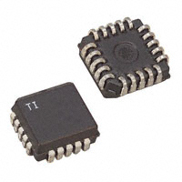
PLCC-20 & LCC-20
(Top View)
Q & L Packages
SOIC-16 (Top View)
DW Package
PACKAGE PIN FUNCTION
FUNCTION
PIN
N/C
INV
NI
E/A Out
Clock
N/C
RT
CT
Ramp
Soft Start
N/C
ILIM/SD
Gnd
Out A
Pwr Gnd
N/C
VC
Out B
VCC
VREF 5.1V
THERMAL RATINGS TABLE
Package
DIL-16J
DIL-16N
PLCC-20
LCC-20
SOIC-16
QJA
80-120
90(1)
43-75(1)
70-80
50-120(1)
QJC
28(2)
45
34
20(2)
35
Q
Q
2
1
2
3
4
5
6
7
8
9
10
11
12
13
14
15
16
17
18
19
20
�UC1825
UC2825
UC3825
ELECTRICAL CHARACTERISTICS: Unless otherwise stated, these specifications apply for , RT = 3.65k, CT = 1nF, VCC
= 15V, -55°C
很抱歉,暂时无法提供与“UC2825QG3”相匹配的价格&库存,您可以联系我们找货
免费人工找货