�
�������� �������� �������� ������
�� �������� �������� �������� ������
�
�
� �
� ���� � ����� ���
SLUS317B − JANUARY 2000 − REVISED FEBRUARY 2004
D
D
D
D
D
D
D
D
Fast Transient Response
10-mA to 3-A Load Current
Short Circuit Protection
Maximum Dropout of 450-mV at 3-A Load
Current
Separate Bias and VIN Pins
Available in Adjustable or Fixed-Output
Voltages
5-Pin Package Allows Kelvin Sensing of
Load Voltage
Reverse Current Protection
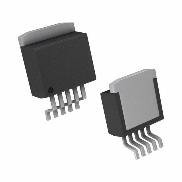
5-PIN TO-220
T PACKAGE (TOP VIEW)
5-PIN TO-263
TD PACKAGE
(TOP VIEW)
Note: Tab = Ground
description
The UC382 is a low-dropout-linear regulator providing a quick response to fast load changes. Combined with
its precision onboard reference, the UC382 excels at driving GTL and BTL buses. Due to its fast response to
load transients, the total capacitance required to decouple the regulator’s output can be significantly decreased
when compared to standard LDO linear regulators.
Dropout voltage (VIN to VOUT) is only 450 mV maximum at 100°C and 350 mV typical at 3-A load.
The onboard bandgap reference is stable with temperature and scaled for a 1.2-V input to the internal-power
amplifier. The UC382 is available in fixed-output voltages of 1.5 V, 2.1 V, or 2.5 V. The output voltage of the
adjustable version can be set with two external resistors. If the external resistors are omitted, the output voltage
defaults to 1.2 V.
block diagram
VB
1
UC382−ADJ
UC382−1 (1.5 V)
UC382−2 (2.1 V)
UC382−3 (2.5 V)
R1
R2
OPEN
2k
2k
2k
0
500 Ω
1.5 k Ω
2.16 k Ω
THERMAL
SHUTDOWN
2
1.2 V
BANDGAP
REFERENCE
VIN
+
R2
R1
SHORT
CIRCUIT
SENSE
3
5
4
GND
ADJ
VOUT
UDG-00080
Please be aware that an important notice concerning availability, standard warranty, and use in critical applications of
Texas Instruments semiconductor products and disclaimers thereto appears at the end of this data sheet.
All trademarks are the property of their respective owners.
Copyright 2000−2004, Texas Instruments Incorporated
���
������
� ����������� �! "#��$�� �! �� %#&'�"����� (��$)
���(#"�! "������ �� !%$"���"�����! %$� �*$ �$��! �� �$+�! ��!��#�$��!
!���(��( ,������-) ���(#"���� %��"$!!��. (�$! ��� �$"$!!���'- ��"'#($
�$!���. �� �'' %����$�$�!)
POST OFFICE BOX 655303
• DALLAS, TEXAS 75265
1
��������� �������� �������� ������
�� �������� �������� �������� ������
�
�
� �
� ���� � ����� ���
�
SLUS317B − JANUARY 2000 − REVISED FEBRUARY 2004
absolute maximum ratings over operating free-air temperature (unless otherwise noted)†}
VB . . . . . . . . . . . . . . . . . . . . . . . . . . . . . . . . . . . . . . . . . . . . . . . . . . . . . . . . . . . . . . . . . . . . . . . . . . . . . . . . . . . . . . . 13 V
VIN . . . . . . . . . . . . . . . . . . . . . . . . . . . . . . . . . . . . . . . . . . . . . . . . . . . . . . . . . . . . . . . . . . . . . . . . . . . . . . . . . . . . . 7.5 V
Output voltage . . . . . . . . . . . . . . . . . . . . . . . . . . . . . . . . . . . . . . . . . . . . . . . . . . . . . . . . . . . . . . . . . . . . . 1.2 V to 6.0 V
Storage temperature, Tstg . . . . . . . . . . . . . . . . . . . . . . . . . . . . . . . . . . . . . . . . . . . . . . . . . . . . . . . . . −65°C to 150°C
Junction temperature, TJ . . . . . . . . . . . . . . . . . . . . . . . . . . . . . . . . . . . . . . . . . . . . . . . . . . . . . . . . . . −55°C to 150°C
Lead temperature (soldering, 10 seconds) . . . . . . . . . . . . . . . . . . . . . . . . . . . . . . . . . . . . . . . . . . . . . . . . . . 300°C
† Stresses beyond those listed under “absolute maximum ratings” may cause permanent damage to the device. These are stress ratings only, and
functional operation of the device at these or any other conditions beyond those indicated under “recommended operating conditions” is not
implied. Exposure to absolute-maximum-rated conditions for extended periods may affect device reliability.
} Currents are positive into, negative out of the specified terminal. Consult Packaging Section of Databook for thermal limitations and
considerations of packages.
AVAILABLE OPTIONS(1)
PACKAGED DEVICES
TO−263 (TD)(2)
TO-220 (T)
TJ
OUTPUT VOLTAGE
OUTPUT VOLTAGE
1.5 V
2.1 V
2.5 V
1.2 V or ADJ
1.5 V
2.1 V
2.5 V
1.2 V or ADJ
–40°C to 100°C
282T-1
282T-2
282T-3
282T-ADJ
282TD-1
282TD-2
282TD-3
282TD-ADJ
0°C to 100°C
382T-1
382T-2
382T-3
382T-ADJ
382TD-1
382TD-2
382TD-3
382TD-ADJ
1. For more package and ordering information, see the Package Option Addendum located at the end of this data sheet.
2. For 50 piece reel, add KTTT (e.g., UC282TDKTTT−1); for 500 piece reel, add TR (e.g., UC282TDTR−1).
electrical characteristics, TA = −40°C to 100°C for the UC282-X series and 0°C to 100°C for the
UC382-X, VB = 5 V, VIN = 3.3 V, VOUT = 2.5 V for the UC382-ADJ, TA = TJ, (unless otherwise stated)
UC382-3 fixed 2.5 V, 3-A family
PARAMETERS
MIN
TYP
MAX
UNITS
UC382-3
TEST CONDITIONS
2.475
2.500
2.525
V
Output voltage (IVOUT = 100 mA)
UC282-3
2.450
2.500
2.525
V
Load regulation
IVOUT = 10 mA to 3 A
0.5
4
80
100
VIN PSSR
VB PSSR
VIN dropout voltage = VIN−VOUT
VB dropout = VB−VOUT
50
dB
60
dB
IVOUT = 3 A,
IVOUT = 3 A,
TJ = 25°C
UC382-3
350
425
mV
350
450
mV
IVOUT = 3 A,
IVOUT = 3 A,
UC282-3
350
500
mV
UC382-3
1.8
2.10
V
IVOUT = 3 A,
UC282-3
1.8
2.20
V
Short circuit current limit
3.3
VB current
IVOUT = 10 mA
IVOUT = 3 A
VIN current
IVOUT = 3 A
2
mV
POST OFFICE BOX 655303
2.94
• DALLAS, TEXAS 75265
4.5
A
6
11
mA
18
60
mA
2.97
A
��
�������� �������� �������� ������
�� �������� �������� �������� ������
�
�
� �
� ���� � ����� ���
SLUS317B − JANUARY 2000 − REVISED FEBRUARY 2004
electrical characteristics, TA = −40°C to 100°C for the UC282-X series and 0°C to 100°C for the
UC382-X, VB = 5 V, VIN = 3.3 V, VOUT = 2.5 V for the UC382-ADJ, TA = TJ, (unless otherwise stated)
UC382-2 fixed 2.1 V, 3-A family
PARAMETERS
MIN
TYP
MAX
UNITS
UC382-2
TEST CONDITIONS
2.079
2.100
2.121
V
Output voltage (IVOUT = 100 mA)
UC282-2
2.058
2.100
2.121
V
Load regulation
IVOUT = 10 mA to 3 A
0.5
4
80
100
VIN PSSR
VB PSSR
52
VIN dropout voltage = VIN−VOUT
VB dropout = VB−VOUT
mV
dB
62
dB
IVOUT = 3 A,
IVOUT = 3 A,
TJ = 25°C
UC382-2
350
425
mV
350
450
mV
IVOUT = 3 A,
IVOUT = 3 A,
UC282-2
350
500
mV
UC382-2
1.8
2.10
V
IVOUT = 3 A,
UC282-2
1.8
2.20
V
Short circuit current limit
3.3
VB current
IVOUT = 10 mA
IVOUT = 3 A
VIN current
IVOUT = 3 A
2.94
4.5
A
6
11
mA
18
60
mA
2.97
A
UC382-1 fixed 1.5 V, 3-A family
PARAMETERS
MIN
TYP
MAX
UNITS
UC382-1
TEST CONDITIONS
1.485
1.500
1.515
V
Output voltage (IVOUT = 100 mA)
UC282-1
1.470
1.500
1.515
Load regulation
IVOUT = 10 mA to 3 A
0.5
4
VIN PSSR
80
VB PSSR
VIN dropout voltage = VIN−VOUT
VB dropout = VB−VOUT
55
100
V
mV
dB
65
dB
IVOUT = 3 A,
IVOUT = 3 A,
TJ = 25°C
UC382-1
350
425
mV
350
450
mV
IVOUT = 3 A,
IVOUT = 3 A,
UC282-1
350
500
mV
UC382-1
1.8
2.10
V
IVOUT = 3 A,
UC282-1
1.8
2.20
V
Short circuit current limit
3.3
VB current
IVOUT = 10 mA
IVOUT = 3 A
VIN current
IVOUT = 3 A
POST OFFICE BOX 655303
2.94
• DALLAS, TEXAS 75265
4.5
A
6
11
mA
18
60
mA
2.97
A
3
��������� �������� �������� ������
�� �������� �������� �������� ������
�
�
� �
� ���� � ����� ���
�
SLUS317B − JANUARY 2000 − REVISED FEBRUARY 2004
electrical characteristics, TA = −40°C to 100°C for the UC282-X series and 0°C to 100°C for the
UC382-X, VB = 5 V, VIN = 3.3 V, VOUT = 2.5 V for the UC382-ADJ, TA = TJ, (unless otherwise stated)
UC382-ADJ adjustable, 3-A family
PARAMETERS
ADJ voltage (IVOUT = 100 mA)
Load regulation
MIN
TYP
MAX
UNITS
UC382-ADJ
TEST CONDITIONS
1.188
1.200
1.212
V
UC282-ADJ
1.176
1.200
1.212
V
0.5
4
80
100
VIN PSSR
IVOUT = 10 mA to 3 A
VOUT programmed for 2.5 V
VB PSSR
VOUT programmed for 2.5 V
TJ = 25°C
UC382-ADJ
350
425
mV
VIN dropout voltage = VIN−VOUT
IVOUT = 3 A,
IVOUT = 3 A,
350
450
mV
IVOUT = 3 A,
IVOUT = 3 A,
UC282-ADJ
350
500
mV
UC382-ADJ
1.8
2.10
V
IVOUT = 3 A,
UC282-ADJ
1.8
2.20
V
VB dropout = VB−VOUT
50
Short circuit current limit
VB current
VIN current
IVOUT = 3 A
2.94
dB
60
3.3
IVOUT = 10 mA
IVOUT = 3 A
mV
dB
4.5
A
6
11
mA
18
60
mA
2.97
A
pin descriptions
ADJ: In the adjustable version, the user programs the output voltage with two external resistors. The resistors
should be 0.1% for high accuracy. The output amplifier is configured as a non-inverting-operational amplifier.
The resistors should meet the criteria of R3 || R4 < 100 Ω. Connect ADJ to VOUT for an output voltage of 1.2 V.
Note that the point at which the feedback network is connected to the output is the Kelvin sense point. For -1,
-2, and -3 versions, ADJ pin is tied to VOUT to obtain specified output voltage.
GND: For accurate results, the GND pin should be referenced to the load ground.
VB: Supplies power to all circuits of the regulator except the collector of the output-power transistor. The 2-V
headroom from VB to VOUT allows the use of a Darlington output stage for inherently-low-output impedance
and fast response. (Dropout is derated for junction temperatures below 0°C.)
VIN: Supplies the current to the collector of the output-power transistor only. The dropout (VIN−VOUT) is under
100 mV for light loads; maximum dropout is 450 mV at 3 A for TJ = 0°C to 100°C. (Dropout is derated for junction
temperatures over 100°C.) At full load, the majority of the VB current is going to the load.
VOUT: This pin should be connected to the load via a low impedance path. Avoid connectors which add
significant inductance and resistance. Note that even though a Kelvin sense is available through a 5-pin
package, care must be taken since voltage drops along wire traces add to the dropout voltage.
4
POST OFFICE BOX 655303
• DALLAS, TEXAS 75265
��������� �������� �������� ������
�� �������� �������� �������� ������
�
�
� �
� ���� � ����� ���
�
SLUS317B − JANUARY 2000 − REVISED FEBRUARY 2004
pin descriptions (continued)
DROPOUT VOLTAGE (VB − VOUT)
vs
LOAD CURRENT
DROPOUT VOLTAGE (VIN − VOUT)
vs
LOAD CURRENT
1.9
400
VDO - Dropout Voltage - mV
VDO - Dropout Voltage - V
TJ = 275C
1.8
1.7
1.6
0
1
2
3
TJ = 275C
300
200
100
100 mA
IL − Load Current − A
1A
2A
3A
IL - Load Current - A
Figure 1
Figure 2
APPLICATION INFORMATION
The UC382 is easy to use. The adjustable version requires two 0.1% resistors to set the output voltage. The
fixed versions of the UC382 require no external resistors. All versions of the UC382 require decoupling
capacitors on the input and output. In a typical application, VB and VIN are driven from switching power supplies
which may have large filter capacitors at their outputs. If the UC382 is further than 12 inches from the power
supply, it is recommended to add local decoupling as close as possible to the linear regulator.
Decouple the output of the UC382 with at least 100 µF of high-quality tantalum or Sanyo OSCON capacitors
close to the VOUT pin for maximum stability. Many applications involving Ultra-Fast GTL or BTL applications
require additional capacitance close to the load. The exact amount will vary according to speed and magnitude
of the load transients and the tolerance allowed for transients on VOUT. When specifying the decoupling
capacitors, the series resistance of the capacitor bank is an important factor in its ability to filter load transients.
The UC382 allows for Kelvin sensing the voltage at the load. This improves regulation performance and
eliminates the voltage drops due to wire-trace resistance. This voltage drop must be added to the headroom
(VIN to VOUT and VB to VOUT). The dropout of 450 mV is measured at the pins and does not include additional
drops due to trace resistance. The minimum load current is 10 mA.
Two or more UC382’s may be used in parallel. While stable, this arrangement does degrade the transient
response.
POST OFFICE BOX 655303
• DALLAS, TEXAS 75265
5
��������� �������� �������� ������
�� �������� �������� �������� ������
�
�
� �
� ���� � ����� ���
�
SLUS317B − JANUARY 2000 − REVISED FEBRUARY 2004
OPEN LOOP PHASE
vs
FREQUENCY
OPEN LOOP GAIN
vs
FREQUENCY
0
70
60
40
Phase - deg
Gain - dB
50
30
−90
20
10
0
−180
−10
100
1k
10 k
100 k
1M
10 M
100
1k
10 k
f − Frequency − Hz
f − Frequency − Hz
PSRR - Power Supply Rejection Ratio (VB INPUT) − dB
Figure 3
Figure 4
POWER SUPPLY REJECTION RATIO (VB INPUT)
vs
FREQUENCY
60
50
40
30
20
10
0
100
1k
10 k
100 k
1M
f − Frequency − Hz
Figure 5
6
100 k
POST OFFICE BOX 655303
• DALLAS, TEXAS 75265
10 M
1M
10 M
��������� �������� �������� ������
�� �������� �������� �������� ������
�
�
� �
� ���� � ����� ���
�
SLUS317B − JANUARY 2000 − REVISED FEBRUARY 2004
APPLICATION INFORMATION
5V
1 µF
CER
1
3.3 V
2
+
VIN
4.7 µF
TANT
VB
VOUT
4
+
100 µF
TANT
UC382−ADJ
GND
ADJ
IRF
520
VO = 1.2 V
121 Ω
R1
PULSE
GENERATOR
5
3
UDG-00081
Figure 6. Transient Test Circuit
10 mA to 3 A/ms Load Transient Response
∆
µ
Figure 7
POST OFFICE BOX 655303
• DALLAS, TEXAS 75265
7
��������� �������� �������� ������
�� �������� �������� �������� ������
�
�
� �
� ���� � ����� ���
�
SLUS317B − JANUARY 2000 − REVISED FEBRUARY 2004
APPLICATION INFORMATION
+5 V
+ 4.7 µF
CER
KELVIN
SENSE
POINT
1
+3.3 V
2
VB
VIN
+ 4.7 µF
VOUT
R3
60 Ω
UC382−ADJ
TANT
GND
ADJ
+1.8 V
OUTPUT
4
5
+ 330 µF
OSCON
2.2 µF
CER
R4
120 Ω
3
UDG-00082
Figure 8. Typical UC382-ADJ Application
+5 V
+
4.7 µF
KELVIN
SENSE
POINT
1
2
VIN
VB
VOUT
+ 330 µF
OSCON
UC382−1
GND
ADJ
+1.5 V
OUTPUT
4
2.2 µF
CER
5
3
UDG-00083
Figure 9. Typical UC382-1, -2, or -3 Application
8
POST OFFICE BOX 655303
• DALLAS, TEXAS 75265
�PACKAGE OPTION ADDENDUM
www.ti.com
24-Jan-2017
PACKAGING INFORMATION
Orderable Device
Status
(1)
Package Type Package Pins Package
Drawing
Qty
Eco Plan
Lead/Ball Finish
MSL Peak Temp
(2)
(6)
(3)
Op Temp (°C)
Device Marking
(4/5)
UC282T-1
ACTIVE
TO-220
KC
5
50
Green (RoHS
& no Sb/Br)
CU SN
N / A for Pkg Type
-40 to 100
UC282T-1
UC282T-2
ACTIVE
TO-220
KC
5
50
Green (RoHS
& no Sb/Br)
CU SN
N / A for Pkg Type
-40 to 100
UC282T-2
UC282T-3
ACTIVE
TO-220
KC
5
50
Green (RoHS
& no Sb/Br)
CU SN
N / A for Pkg Type
-40 to 100
UC282T-3
UC282T-ADJ
ACTIVE
TO-220
KC
5
50
Green (RoHS
& no Sb/Br)
CU SN
N / A for Pkg Type
-40 to 100
UC282T-ADJ
UC282TD-1
OBSOLETE
DDPAK/
TO-263
KTT
5
TBD
Call TI
Call TI
-40 to 100
UC282TD-2
OBSOLETE
DDPAK/
TO-263
KTT
5
TBD
Call TI
Call TI
-40 to 100
UC282TD-3
OBSOLETE
DDPAK/
TO-263
KTT
5
TBD
Call TI
Call TI
-40 to 100
UC282TD-ADJ
OBSOLETE
DDPAK/
TO-263
KTT
5
TBD
Call TI
Call TI
-40 to 100
UC282TDKTTT-1
ACTIVE
DDPAK/
TO-263
KTT
5
Green (RoHS
& no Sb/Br)
CU SN
Level-2-260C-1 YEAR
-40 to 100
UC282TD-1
UC282TDKTTT-2
OBSOLETE
DDPAK/
TO-263
KTT
5
TBD
Call TI
Call TI
-40 to 100
UC282TD-2
UC282TDKTTT-2G3
ACTIVE
DDPAK/
TO-263
KTT
5
TBD
Call TI
Call TI
-40 to 100
UC282TDKTTT-3
ACTIVE
DDPAK/
TO-263
KTT
5
50
Green (RoHS
& no Sb/Br)
CU SN
Level-2-260C-1 YEAR
-40 to 100
UC282TD-3
UC282TDKTTT-ADJ
ACTIVE
DDPAK/
TO-263
KTT
5
50
Green (RoHS
& no Sb/Br)
CU SN
Level-2-260C-1 YEAR
-40 to 100
UC282TD-ADJ
UC282TDKTTT-ADJG3
ACTIVE
DDPAK/
TO-263
KTT
5
50
Green (RoHS
& no Sb/Br)
CU SN
Level-2-260C-1 YEAR
-40 to 100
UC282TD-ADJ
UC282TDTR-1
ACTIVE
DDPAK/
TO-263
KTT
5
500
Green (RoHS
& no Sb/Br)
CU SN
Level-2-260C-1 YEAR
-40 to 100
UC282TD-1
UC282TDTR-3
ACTIVE
DDPAK/
TO-263
KTT
5
500
Green (RoHS
& no Sb/Br)
CU SN
Level-2-260C-1 YEAR
-40 to 100
UC282TD-3
UC282TDTR-ADJ
ACTIVE
DDPAK/
TO-263
KTT
5
500
Green (RoHS
& no Sb/Br)
CU SN
Level-2-260C-1 YEAR
-40 to 100
UC282TD-ADJ
50
Addendum-Page 1
Samples
�PACKAGE OPTION ADDENDUM
www.ti.com
24-Jan-2017
Orderable Device
Status
(1)
Package Type Package Pins Package
Drawing
Qty
Eco Plan
Lead/Ball Finish
MSL Peak Temp
(2)
(6)
(3)
Op Temp (°C)
Device Marking
(4/5)
UC382T-1
ACTIVE
TO-220
KC
5
50
Green (RoHS
& no Sb/Br)
CU SN
N / A for Pkg Type
-40 to 100
UC382T-1
UC382T-2
ACTIVE
TO-220
KC
5
50
Green (RoHS
& no Sb/Br)
CU SN
N / A for Pkg Type
0 to 100
UC382T-2
UC382T-3
ACTIVE
TO-220
KC
5
50
Green (RoHS
& no Sb/Br)
CU SN
N / A for Pkg Type
0 to 100
UC382T-3
UC382T-ADJ
ACTIVE
TO-220
KC
5
50
Green (RoHS
& no Sb/Br)
CU SN
N / A for Pkg Type
0 to 100
UC382T-ADJ
UC382T-ADJG3
ACTIVE
TO-220
KC
5
50
Green (RoHS
& no Sb/Br)
CU SN
N / A for Pkg Type
0 to 100
UC382T-ADJ
UC382TD-1
OBSOLETE
DDPAK/
TO-263
KTT
5
TBD
Call TI
Call TI
-40 to 100
UC382TD-2
OBSOLETE
DDPAK/
TO-263
KTT
5
TBD
Call TI
Call TI
0 to 100
UC382TD-3
OBSOLETE
DDPAK/
TO-263
KTT
5
TBD
Call TI
Call TI
0 to 100
UC382TD-ADJ
OBSOLETE
DDPAK/
TO-263
KTT
5
TBD
Call TI
Call TI
0 to 100
UC382TDKTTT-2
ACTIVE
DDPAK/
TO-263
KTT
5
50
Green (RoHS
& no Sb/Br)
CU SN
Level-2-260C-1 YEAR
0 to 70
UC382TD-2
UC382TDKTTT-3
ACTIVE
DDPAK/
TO-263
KTT
5
50
Green (RoHS
& no Sb/Br)
CU SN
Level-2-260C-1 YEAR
0 to 70
UC382TD-3
UC382TDKTTT-ADJ
ACTIVE
DDPAK/
TO-263
KTT
5
50
Green (RoHS
& no Sb/Br)
CU SN
Level-2-260C-1 YEAR
0 to 100
UC382TD-ADJ
UC382TDKTTT-ADJG3
ACTIVE
DDPAK/
TO-263
KTT
5
TBD
Call TI
Call TI
0 to 100
UC382TDTR-3
ACTIVE
DDPAK/
TO-263
KTT
5
500
Green (RoHS
& no Sb/Br)
CU SN
Level-2-260C-1 YEAR
0 to 100
UC382TD-3
UC382TDTR-ADJ
ACTIVE
DDPAK/
TO-263
KTT
5
500
Green (RoHS
& no Sb/Br)
CU SN
Level-2-260C-1 YEAR
0 to 100
UC382TD-ADJ
UC382TDTR-ADJG3
ACTIVE
DDPAK/
TO-263
KTT
5
500
Green (RoHS
& no Sb/Br)
CU SN
Level-2-260C-1 YEAR
0 to 100
UC382TD-ADJ
(1)
The marketing status values are defined as follows:
ACTIVE: Product device recommended for new designs.
LIFEBUY: TI has announced that the device will be discontinued, and a lifetime-buy period is in effect.
NRND: Not recommended for new designs. Device is in production to support existing customers, but TI does not recommend using this part in a new design.
Addendum-Page 2
Samples
�PACKAGE OPTION ADDENDUM
www.ti.com
24-Jan-2017
PREVIEW: Device has been announced but is not in production. Samples may or may not be available.
OBSOLETE: TI has discontinued the production of the device.
(2)
Eco Plan - The planned eco-friendly classification: Pb-Free (RoHS), Pb-Free (RoHS Exempt), or Green (RoHS & no Sb/Br) - please check http://www.ti.com/productcontent for the latest availability
information and additional product content details.
TBD: The Pb-Free/Green conversion plan has not been defined.
Pb-Free (RoHS): TI's terms "Lead-Free" or "Pb-Free" mean semiconductor products that are compatible with the current RoHS requirements for all 6 substances, including the requirement that
lead not exceed 0.1% by weight in homogeneous materials. Where designed to be soldered at high temperatures, TI Pb-Free products are suitable for use in specified lead-free processes.
Pb-Free (RoHS Exempt): This component has a RoHS exemption for either 1) lead-based flip-chip solder bumps used between the die and package, or 2) lead-based die adhesive used between
the die and leadframe. The component is otherwise considered Pb-Free (RoHS compatible) as defined above.
Green (RoHS & no Sb/Br): TI defines "Green" to mean Pb-Free (RoHS compatible), and free of Bromine (Br) and Antimony (Sb) based flame retardants (Br or Sb do not exceed 0.1% by weight
in homogeneous material)
(3)
MSL, Peak Temp. - The Moisture Sensitivity Level rating according to the JEDEC industry standard classifications, and peak solder temperature.
(4)
There may be additional marking, which relates to the logo, the lot trace code information, or the environmental category on the device.
(5)
Multiple Device Markings will be inside parentheses. Only one Device Marking contained in parentheses and separated by a "~" will appear on a device. If a line is indented then it is a continuation
of the previous line and the two combined represent the entire Device Marking for that device.
(6)
Lead/Ball Finish - Orderable Devices may have multiple material finish options. Finish options are separated by a vertical ruled line. Lead/Ball Finish values may wrap to two lines if the finish
value exceeds the maximum column width.
Important Information and Disclaimer:The information provided on this page represents TI's knowledge and belief as of the date that it is provided. TI bases its knowledge and belief on information
provided by third parties, and makes no representation or warranty as to the accuracy of such information. Efforts are underway to better integrate information from third parties. TI has taken and
continues to take reasonable steps to provide representative and accurate information but may not have conducted destructive testing or chemical analysis on incoming materials and chemicals.
TI and TI suppliers consider certain information to be proprietary, and thus CAS numbers and other limited information may not be available for release.
In no event shall TI's liability arising out of such information exceed the total purchase price of the TI part(s) at issue in this document sold by TI to Customer on an annual basis.
Addendum-Page 3
�PACKAGE MATERIALS INFORMATION
www.ti.com
24-Jan-2017
TAPE AND REEL INFORMATION
*All dimensions are nominal
Device
Package Package Pins
Type Drawing
SPQ
Reel
Reel
A0
Diameter Width (mm)
(mm) W1 (mm)
B0
(mm)
K0
(mm)
P1
(mm)
W
Pin1
(mm) Quadrant
UC282TDKTTT-1
DDPAK/
TO-263
KTT
5
50
330.0
24.4
10.6
15.6
4.9
16.0
24.0
Q2
UC282TDKTTT-3
DDPAK/
TO-263
KTT
5
50
330.0
24.4
10.6
15.6
4.9
16.0
24.0
Q2
UC282TDKTTT-ADJ
DDPAK/
TO-263
KTT
5
50
330.0
24.4
10.6
15.6
4.9
16.0
24.0
Q2
UC282TDTR-1
DDPAK/
TO-263
KTT
5
500
330.0
24.4
10.6
15.6
4.9
16.0
24.0
Q2
UC282TDTR-3
DDPAK/
TO-263
KTT
5
500
330.0
24.4
10.6
15.6
4.9
16.0
24.0
Q2
UC282TDTR-ADJ
DDPAK/
TO-263
KTT
5
500
330.0
24.4
10.6
15.6
4.9
16.0
24.0
Q2
UC382TDKTTT-2
DDPAK/
TO-263
KTT
5
50
330.0
24.4
10.6
15.6
4.9
16.0
24.0
Q2
UC382TDKTTT-3
DDPAK/
TO-263
KTT
5
50
330.0
24.4
10.6
15.6
4.9
16.0
24.0
Q2
UC382TDKTTT-ADJ
DDPAK/
TO-263
KTT
5
50
330.0
24.4
10.6
15.6
4.9
16.0
24.0
Q2
UC382TDTR-3
DDPAK/
TO-263
KTT
5
500
330.0
24.4
10.6
15.6
4.9
16.0
24.0
Q2
UC382TDTR-ADJ
DDPAK/
KTT
5
500
330.0
24.4
10.6
15.6
4.9
16.0
24.0
Q2
Pack Materials-Page 1
�PACKAGE MATERIALS INFORMATION
www.ti.com
24-Jan-2017
Device
Package Package Pins
Type Drawing
SPQ
Reel
Reel
A0
Diameter Width (mm)
(mm) W1 (mm)
B0
(mm)
K0
(mm)
P1
(mm)
W
Pin1
(mm) Quadrant
TO-263
*All dimensions are nominal
Device
Package Type
Package Drawing
Pins
SPQ
Length (mm)
Width (mm)
Height (mm)
UC282TDKTTT-1
DDPAK/TO-263
KTT
5
50
367.0
367.0
45.0
UC282TDKTTT-3
DDPAK/TO-263
KTT
5
50
367.0
367.0
45.0
UC282TDKTTT-ADJ
DDPAK/TO-263
KTT
5
50
367.0
367.0
45.0
UC282TDTR-1
DDPAK/TO-263
KTT
5
500
367.0
367.0
45.0
UC282TDTR-3
DDPAK/TO-263
KTT
5
500
367.0
367.0
45.0
UC282TDTR-ADJ
DDPAK/TO-263
KTT
5
500
367.0
367.0
45.0
UC382TDKTTT-2
DDPAK/TO-263
KTT
5
50
367.0
367.0
45.0
UC382TDKTTT-3
DDPAK/TO-263
KTT
5
50
367.0
367.0
45.0
UC382TDKTTT-ADJ
DDPAK/TO-263
KTT
5
50
367.0
367.0
45.0
UC382TDTR-3
DDPAK/TO-263
KTT
5
500
367.0
367.0
45.0
UC382TDTR-ADJ
DDPAK/TO-263
KTT
5
500
367.0
367.0
45.0
Pack Materials-Page 2
�PACKAGE OUTLINE
KC0005A
TO-220 - 16.51 mm max height
SCALE 0.850
TO-220
4.83
4.06
10.67
9.65
3.05
2.54
B
1.40
1.14
A
6.86
5.69
3.71-3.96
8.89
6.86
(6.275)
12.88
10.08
OPTIONAL
CHAMFER
16.51
MAX
2X (R1)
OPTIONAL
9.25
7.67
C
(4.25)
PIN 1 ID
(OPTIONAL)
NOTE 3
14.73
12.29
1
5X
0.25
5
0.61
0.30
1.02
0.64
C A B
3.05
2.03
4X 1.7
6.8
1
5
4215009/A 01/2017
NOTES:
1. All controlling linear dimensions are in inches. Dimensions in brackets are in millimeters. Any dimension in brackets or parenthesis are for
reference only. Dimensioning and tolerancing per ASME Y14.5M.
2. This drawing is subject to change without notice.
3. Shape may vary per different assembly sites.
www.ti.com
�EXAMPLE BOARD LAYOUT
KC0005A
TO-220 - 16.51 mm max height
TO-220
4X (1.45)
PKG
0.07 MAX
ALL AROUND
0.07 MAX
ALL AROUND
METAL
TYP
(1.45)
PKG
(2)
4X (2)
1
(R0.05) TYP
5X ( 1.2)
SOLDER MASK
OPENING, TYP
(1.7) TYP
5
FULL R
TYP
(6.8)
LAND PATTERN
NON-SOLDER MASK DEFINED
SCALE:12X
4215009/A 01/2017
www.ti.com
���IMPORTANT NOTICE FOR TI DESIGN INFORMATION AND RESOURCES
Texas Instruments Incorporated (‘TI”) technical, application or other design advice, services or information, including, but not limited to,
reference designs and materials relating to evaluation modules, (collectively, “TI Resources”) are intended to assist designers who are
developing applications that incorporate TI products; by downloading, accessing or using any particular TI Resource in any way, you
(individually or, if you are acting on behalf of a company, your company) agree to use it solely for this purpose and subject to the terms of
this Notice.
TI’s provision of TI Resources does not expand or otherwise alter TI’s applicable published warranties or warranty disclaimers for TI
products, and no additional obligations or liabilities arise from TI providing such TI Resources. TI reserves the right to make corrections,
enhancements, improvements and other changes to its TI Resources.
You understand and agree that you remain responsible for using your independent analysis, evaluation and judgment in designing your
applications and that you have full and exclusive responsibility to assure the safety of your applications and compliance of your applications
(and of all TI products used in or for your applications) with all applicable regulations, laws and other applicable requirements. You
represent that, with respect to your applications, you have all the necessary expertise to create and implement safeguards that (1)
anticipate dangerous consequences of failures, (2) monitor failures and their consequences, and (3) lessen the likelihood of failures that
might cause harm and take appropriate actions. You agree that prior to using or distributing any applications that include TI products, you
will thoroughly test such applications and the functionality of such TI products as used in such applications. TI has not conducted any
testing other than that specifically described in the published documentation for a particular TI Resource.
You are authorized to use, copy and modify any individual TI Resource only in connection with the development of applications that include
the TI product(s) identified in such TI Resource. NO OTHER LICENSE, EXPRESS OR IMPLIED, BY ESTOPPEL OR OTHERWISE TO
ANY OTHER TI INTELLECTUAL PROPERTY RIGHT, AND NO LICENSE TO ANY TECHNOLOGY OR INTELLECTUAL PROPERTY
RIGHT OF TI OR ANY THIRD PARTY IS GRANTED HEREIN, including but not limited to any patent right, copyright, mask work right, or
other intellectual property right relating to any combination, machine, or process in which TI products or services are used. Information
regarding or referencing third-party products or services does not constitute a license to use such products or services, or a warranty or
endorsement thereof. Use of TI Resources may require a license from a third party under the patents or other intellectual property of the
third party, or a license from TI under the patents or other intellectual property of TI.
TI RESOURCES ARE PROVIDED “AS IS” AND WITH ALL FAULTS. TI DISCLAIMS ALL OTHER WARRANTIES OR
REPRESENTATIONS, EXPRESS OR IMPLIED, REGARDING TI RESOURCES OR USE THEREOF, INCLUDING BUT NOT LIMITED TO
ACCURACY OR COMPLETENESS, TITLE, ANY EPIDEMIC FAILURE WARRANTY AND ANY IMPLIED WARRANTIES OF
MERCHANTABILITY, FITNESS FOR A PARTICULAR PURPOSE, AND NON-INFRINGEMENT OF ANY THIRD PARTY INTELLECTUAL
PROPERTY RIGHTS.
TI SHALL NOT BE LIABLE FOR AND SHALL NOT DEFEND OR INDEMNIFY YOU AGAINST ANY CLAIM, INCLUDING BUT NOT
LIMITED TO ANY INFRINGEMENT CLAIM THAT RELATES TO OR IS BASED ON ANY COMBINATION OF PRODUCTS EVEN IF
DESCRIBED IN TI RESOURCES OR OTHERWISE. IN NO EVENT SHALL TI BE LIABLE FOR ANY ACTUAL, DIRECT, SPECIAL,
COLLATERAL, INDIRECT, PUNITIVE, INCIDENTAL, CONSEQUENTIAL OR EXEMPLARY DAMAGES IN CONNECTION WITH OR
ARISING OUT OF TI RESOURCES OR USE THEREOF, AND REGARDLESS OF WHETHER TI HAS BEEN ADVISED OF THE
POSSIBILITY OF SUCH DAMAGES.
You agree to fully indemnify TI and its representatives against any damages, costs, losses, and/or liabilities arising out of your noncompliance with the terms and provisions of this Notice.
This Notice applies to TI Resources. Additional terms apply to the use and purchase of certain types of materials, TI products and services.
These include; without limitation, TI’s standard terms for semiconductor products http://www.ti.com/sc/docs/stdterms.htm), evaluation
modules, and samples (http://www.ti.com/sc/docs/sampterms.htm).
Mailing Address: Texas Instruments, Post Office Box 655303, Dallas, Texas 75265
Copyright © 2017, Texas Instruments Incorporated
�


 工商网监
湘ICP备2023018690号
工商网监
湘ICP备2023018690号
