�
�������� �������� �������� ������
�� �������� �������� �������� ������
�
�
� �
� ���� � ����� ���
SLUS317B − JANUARY 2000 − REVISED FEBRUARY 2004
D
D
D
D
D
D
D
D
Fast Transient Response
10-mA to 3-A Load Current
Short Circuit Protection
Maximum Dropout of 450-mV at 3-A Load
Current
Separate Bias and VIN Pins
Available in Adjustable or Fixed-Output
Voltages
5-Pin Package Allows Kelvin Sensing of
Load Voltage
Reverse Current Protection
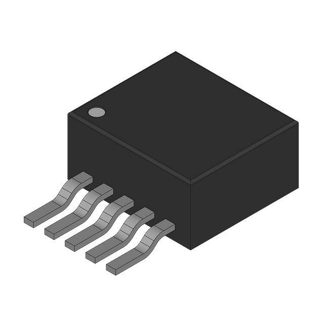
5-PIN TO-220
T PACKAGE (TOP VIEW)
5-PIN TO-263
TD PACKAGE
(TOP VIEW)
Note: Tab = Ground
description
The UC382 is a low-dropout-linear regulator providing a quick response to fast load changes. Combined with
its precision onboard reference, the UC382 excels at driving GTL and BTL buses. Due to its fast response to
load transients, the total capacitance required to decouple the regulator’s output can be significantly decreased
when compared to standard LDO linear regulators.
Dropout voltage (VIN to VOUT) is only 450 mV maximum at 100°C and 350 mV typical at 3-A load.
The onboard bandgap reference is stable with temperature and scaled for a 1.2-V input to the internal-power
amplifier. The UC382 is available in fixed-output voltages of 1.5 V, 2.1 V, or 2.5 V. The output voltage of the
adjustable version can be set with two external resistors. If the external resistors are omitted, the output voltage
defaults to 1.2 V.
block diagram
VB
1
UC382−ADJ
UC382−1 (1.5 V)
UC382−2 (2.1 V)
UC382−3 (2.5 V)
R1
R2
OPEN
2k
2k
2k
0
500 Ω
1.5 k Ω
2.16 k Ω
THERMAL
SHUTDOWN
2
1.2 V
BANDGAP
REFERENCE
VIN
+
R2
R1
SHORT
CIRCUIT
SENSE
3
5
4
GND
ADJ
VOUT
UDG-00080
Please be aware that an important notice concerning availability, standard warranty, and use in critical applications of
Texas Instruments semiconductor products and disclaimers thereto appears at the end of this data sheet.
All trademarks are the property of their respective owners.
Copyright 2000−2004, Texas Instruments Incorporated
���
������
� ����������� �! "#��$�� �! �� %#&'�"����� (��$)
���(#"�! "������ �� !%$"���"�����! %$� �*$ �$��! �� �$+�! ��!��#�$��!
!���(��( ,������-) ���(#"���� %��"$!!��. (�$! ��� �$"$!!���'- ��"'#($
�$!���. �� �'' %����$�$�!)
POST OFFICE BOX 655303
• DALLAS, TEXAS 75265
1
��������� �������� �������� ������
�� �������� �������� �������� ������
�
�
� �
� ���� � ����� ���
�
SLUS317B − JANUARY 2000 − REVISED FEBRUARY 2004
absolute maximum ratings over operating free-air temperature (unless otherwise noted)†}
VB . . . . . . . . . . . . . . . . . . . . . . . . . . . . . . . . . . . . . . . . . . . . . . . . . . . . . . . . . . . . . . . . . . . . . . . . . . . . . . . . . . . . . . . 13 V
VIN . . . . . . . . . . . . . . . . . . . . . . . . . . . . . . . . . . . . . . . . . . . . . . . . . . . . . . . . . . . . . . . . . . . . . . . . . . . . . . . . . . . . . 7.5 V
Output voltage . . . . . . . . . . . . . . . . . . . . . . . . . . . . . . . . . . . . . . . . . . . . . . . . . . . . . . . . . . . . . . . . . . . . . 1.2 V to 6.0 V
Storage temperature, Tstg . . . . . . . . . . . . . . . . . . . . . . . . . . . . . . . . . . . . . . . . . . . . . . . . . . . . . . . . . −65°C to 150°C
Junction temperature, TJ . . . . . . . . . . . . . . . . . . . . . . . . . . . . . . . . . . . . . . . . . . . . . . . . . . . . . . . . . . −55°C to 150°C
Lead temperature (soldering, 10 seconds) . . . . . . . . . . . . . . . . . . . . . . . . . . . . . . . . . . . . . . . . . . . . . . . . . . 300°C
† Stresses beyond those listed under “absolute maximum ratings” may cause permanent damage to the device. These are stress ratings only, and
functional operation of the device at these or any other conditions beyond those indicated under “recommended operating conditions” is not
implied. Exposure to absolute-maximum-rated conditions for extended periods may affect device reliability.
} Currents are positive into, negative out of the specified terminal. Consult Packaging Section of Databook for thermal limitations and
considerations of packages.
AVAILABLE OPTIONS(1)
PACKAGED DEVICES
TO−263 (TD)(2)
TO-220 (T)
TJ
OUTPUT VOLTAGE
OUTPUT VOLTAGE
1.5 V
2.1 V
2.5 V
1.2 V or ADJ
1.5 V
2.1 V
2.5 V
1.2 V or ADJ
–40°C to 100°C
282T-1
282T-2
282T-3
282T-ADJ
282TD-1
282TD-2
282TD-3
282TD-ADJ
0°C to 100°C
382T-1
382T-2
382T-3
382T-ADJ
382TD-1
382TD-2
382TD-3
382TD-ADJ
1. For more package and ordering information, see the Package Option Addendum located at the end of this data sheet.
2. For 50 piece reel, add KTTT (e.g., UC282TDKTTT−1); for 500 piece reel, add TR (e.g., UC282TDTR−1).
electrical characteristics, TA = −40°C to 100°C for the UC282-X series and 0°C to 100°C for the
UC382-X, VB = 5 V, VIN = 3.3 V, VOUT = 2.5 V for the UC382-ADJ, TA = TJ, (unless otherwise stated)
UC382-3 fixed 2.5 V, 3-A family
PARAMETERS
MIN
TYP
MAX
UNITS
UC382-3
TEST CONDITIONS
2.475
2.500
2.525
V
Output voltage (IVOUT = 100 mA)
UC282-3
2.450
2.500
2.525
V
Load regulation
IVOUT = 10 mA to 3 A
0.5
4
80
100
VIN PSSR
VB PSSR
VIN dropout voltage = VIN−VOUT
VB dropout = VB−VOUT
50
dB
60
dB
IVOUT = 3 A,
IVOUT = 3 A,
TJ = 25°C
UC382-3
350
425
mV
350
450
mV
IVOUT = 3 A,
IVOUT = 3 A,
UC282-3
350
500
mV
UC382-3
1.8
2.10
V
IVOUT = 3 A,
UC282-3
1.8
2.20
V
Short circuit current limit
3.3
VB current
IVOUT = 10 mA
IVOUT = 3 A
VIN current
IVOUT = 3 A
2
mV
POST OFFICE BOX 655303
2.94
• DALLAS, TEXAS 75265
4.5
A
6
11
mA
18
60
mA
2.97
A
��
�������� �������� �������� ������
�� �������� �������� �������� ������
�
�
� �
� ���� � ����� ���
SLUS317B − JANUARY 2000 − REVISED FEBRUARY 2004
electrical characteristics, TA = −40°C to 100°C for the UC282-X series and 0°C to 100°C for the
UC382-X, VB = 5 V, VIN = 3.3 V, VOUT = 2.5 V for the UC382-ADJ, TA = TJ, (unless otherwise stated)
UC382-2 fixed 2.1 V, 3-A family
PARAMETERS
MIN
TYP
MAX
UNITS
UC382-2
TEST CONDITIONS
2.079
2.100
2.121
V
Output voltage (IVOUT = 100 mA)
UC282-2
2.058
2.100
2.121
V
Load regulation
IVOUT = 10 mA to 3 A
0.5
4
80
100
VIN PSSR
VB PSSR
52
VIN dropout voltage = VIN−VOUT
VB dropout = VB−VOUT
mV
dB
62
dB
IVOUT = 3 A,
IVOUT = 3 A,
TJ = 25°C
UC382-2
350
425
mV
350
450
mV
IVOUT = 3 A,
IVOUT = 3 A,
UC282-2
350
500
mV
UC382-2
1.8
2.10
V
IVOUT = 3 A,
UC282-2
1.8
2.20
V
Short circuit current limit
3.3
VB current
IVOUT = 10 mA
IVOUT = 3 A
VIN current
IVOUT = 3 A
2.94
4.5
A
6
11
mA
18
60
mA
2.97
A
UC382-1 fixed 1.5 V, 3-A family
PARAMETERS
MIN
TYP
MAX
UNITS
UC382-1
TEST CONDITIONS
1.485
1.500
1.515
V
Output voltage (IVOUT = 100 mA)
UC282-1
1.470
1.500
1.515
Load regulation
IVOUT = 10 mA to 3 A
0.5
4
VIN PSSR
80
VB PSSR
VIN dropout voltage = VIN−VOUT
VB dropout = VB−VOUT
55
100
V
mV
dB
65
dB
IVOUT = 3 A,
IVOUT = 3 A,
TJ = 25°C
UC382-1
350
425
mV
350
450
mV
IVOUT = 3 A,
IVOUT = 3 A,
UC282-1
350
500
mV
UC382-1
1.8
2.10
V
IVOUT = 3 A,
UC282-1
1.8
2.20
V
Short circuit current limit
3.3
VB current
IVOUT = 10 mA
IVOUT = 3 A
VIN current
IVOUT = 3 A
POST OFFICE BOX 655303
2.94
• DALLAS, TEXAS 75265
4.5
A
6
11
mA
18
60
mA
2.97
A
3
��������� �������� �������� ������
�� �������� �������� �������� ������
�
�
� �
� ���� � ����� ���
�
SLUS317B − JANUARY 2000 − REVISED FEBRUARY 2004
electrical characteristics, TA = −40°C to 100°C for the UC282-X series and 0°C to 100°C for the
UC382-X, VB = 5 V, VIN = 3.3 V, VOUT = 2.5 V for the UC382-ADJ, TA = TJ, (unless otherwise stated)
UC382-ADJ adjustable, 3-A family
PARAMETERS
ADJ voltage (IVOUT = 100 mA)
Load regulation
MIN
TYP
MAX
UNITS
UC382-ADJ
TEST CONDITIONS
1.188
1.200
1.212
V
UC282-ADJ
1.176
1.200
1.212
V
0.5
4
80
100
VIN PSSR
IVOUT = 10 mA to 3 A
VOUT programmed for 2.5 V
VB PSSR
VOUT programmed for 2.5 V
TJ = 25°C
UC382-ADJ
350
425
mV
VIN dropout voltage = VIN−VOUT
IVOUT = 3 A,
IVOUT = 3 A,
350
450
mV
IVOUT = 3 A,
IVOUT = 3 A,
UC282-ADJ
350
500
mV
UC382-ADJ
1.8
2.10
V
IVOUT = 3 A,
UC282-ADJ
1.8
2.20
V
VB dropout = VB−VOUT
50
Short circuit current limit
VB current
VIN current
IVOUT = 3 A
2.94
dB
60
3.3
IVOUT = 10 mA
IVOUT = 3 A
mV
dB
4.5
A
6
11
mA
18
60
mA
2.97
A
pin descriptions
ADJ: In the adjustable version, the user programs the output voltage with two external resistors. The resistors
should be 0.1% for high accuracy. The output amplifier is configured as a non-inverting-operational amplifier.
The resistors should meet the criteria of R3 || R4 < 100 Ω. Connect ADJ to VOUT for an output voltage of 1.2 V.
Note that the point at which the feedback network is connected to the output is the Kelvin sense point. For -1,
-2, and -3 versions, ADJ pin is tied to VOUT to obtain specified output voltage.
GND: For accurate results, the GND pin should be referenced to the load ground.
VB: Supplies power to all circuits of the regulator except the collector of the output-power transistor. The 2-V
headroom from VB to VOUT allows the use of a Darlington output stage for inherently-low-output impedance
and fast response. (Dropout is derated for junction temperatures below 0°C.)
VIN: Supplies the current to the collector of the output-power transistor only. The dropout (VIN−VOUT) is under
100 mV for light loads; maximum dropout is 450 mV at 3 A for TJ = 0°C to 100°C. (Dropout is derated for junction
temperatures over 100°C.) At full load, the majority of the VB current is going to the load.
VOUT: This pin should be connected to the load via a low impedance path. Avoid connectors which add
significant inductance and resistance. Note that even though a Kelvin sense is available through a 5-pin
package, care must be taken since voltage drops along wire traces add to the dropout voltage.
4
POST OFFICE BOX 655303
• DALLAS, TEXAS 75265
��������� �������� �������� ������
�� �������� �������� �������� ������
�
�
� �
� ���� � ����� ���
�
SLUS317B − JANUARY 2000 − REVISED FEBRUARY 2004
pin descriptions (continued)
DROPOUT VOLTAGE (VB − VOUT)
vs
LOAD CURRENT
DROPOUT VOLTAGE (VIN − VOUT)
vs
LOAD CURRENT
1.9
400
VDO - Dropout Voltage - mV
VDO - Dropout Voltage - V
TJ = 275C
1.8
1.7
1.6
0
1
2
3
TJ = 275C
300
200
100
100 mA
IL − Load Current − A
1A
2A
3A
IL - Load Current - A
Figure 1
Figure 2
APPLICATION INFORMATION
The UC382 is easy to use. The adjustable version requires two 0.1% resistors to set the output voltage. The
fixed versions of the UC382 require no external resistors. All versions of the UC382 require decoupling
capacitors on the input and output. In a typical application, VB and VIN are driven from switching power supplies
which may have large filter capacitors at their outputs. If the UC382 is further than 12 inches from the power
supply, it is recommended to add local decoupling as close as possible to the linear regulator.
Decouple the output of the UC382 with at least 100 µF of high-quality tantalum or Sanyo OSCON capacitors
close to the VOUT pin for maximum stability. Many applications involving Ultra-Fast GTL or BTL applications
require additional capacitance close to the load. The exact amount will vary according to speed and magnitude
of the load transients and the tolerance allowed for transients on VOUT. When specifying the decoupling
capacitors, the series resistance of the capacitor bank is an important factor in its ability to filter load transients.
The UC382 allows for Kelvin sensing the voltage at the load. This improves regulation performance and
eliminates the voltage drops due to wire-trace resistance. This voltage drop must be added to the headroom
(VIN to VOUT and VB to VOUT). The dropout of 450 mV is measured at the pins and does not include additional
drops due to trace resistance. The minimum load current is 10 mA.
Two or more UC382’s may be used in parallel. While stable, this arrangement does degrade the transient
response.
POST OFFICE BOX 655303
• DALLAS, TEXAS 75265
5
��������� �������� �������� ������
�� �������� �������� �������� ������
�
�
� �
� ���� � ����� ���
�
SLUS317B − JANUARY 2000 − REVISED FEBRUARY 2004
OPEN LOOP PHASE
vs
FREQUENCY
OPEN LOOP GAIN
vs
FREQUENCY
0
70
60
40
Phase - deg
Gain - dB
50
30
−90
20
10
0
−180
−10
100
1k
10 k
100 k
1M
10 M
100
1k
10 k
f − Frequency − Hz
f − Frequency − Hz
PSRR - Power Supply Rejection Ratio (VB INPUT) − dB
Figure 3
Figure 4
POWER SUPPLY REJECTION RATIO (VB INPUT)
vs
FREQUENCY
60
50
40
30
20
10
0
100
1k
10 k
100 k
1M
f − Frequency − Hz
Figure 5
6
100 k
POST OFFICE BOX 655303
• DALLAS, TEXAS 75265
10 M
1M
10 M
��������� �������� �������� ������
�� �������� �������� �������� ������
�
�
� �
� ���� � ����� ���
�
SLUS317B − JANUARY 2000 − REVISED FEBRUARY 2004
APPLICATION INFORMATION
5V
1 µF
CER
1
3.3 V
2
+
VIN
4.7 µF
TANT
VB
VOUT
4
+
100 µF
TANT
UC382−ADJ
GND
ADJ
IRF
520
VO = 1.2 V
121 Ω
R1
PULSE
GENERATOR
5
3
UDG-00081
Figure 6. Transient Test Circuit
10 mA to 3 A/ms Load Transient Response
∆
µ
Figure 7
POST OFFICE BOX 655303
• DALLAS, TEXAS 75265
7
��������� �������� �������� ������
�� �������� �������� �������� ������
�
�
� �
� ���� � ����� ���
�
SLUS317B − JANUARY 2000 − REVISED FEBRUARY 2004
APPLICATION INFORMATION
+5 V
+ 4.7 µF
CER
KELVIN
SENSE
POINT
1
+3.3 V
2
VB
VIN
+ 4.7 µF
VOUT
R3
60 Ω
UC382−ADJ
TANT
GND
ADJ
+1.8 V
OUTPUT
4
5
+ 330 µF
OSCON
2.2 µF
CER
R4
120 Ω
3
UDG-00082
Figure 8. Typical UC382-ADJ Application
+5 V
+
4.7 µF
KELVIN
SENSE
POINT
1
2
VIN
VB
VOUT
+ 330 µF
OSCON
UC382−1
GND
ADJ
+1.5 V
OUTPUT
4
2.2 µF
CER
5
3
UDG-00083
Figure 9. Typical UC382-1, -2, or -3 Application
8
POST OFFICE BOX 655303
• DALLAS, TEXAS 75265
�PACKAGE OPTION ADDENDUM
www.ti.com
14-Oct-2022
PACKAGING INFORMATION
Orderable Device
Status
(1)
Package Type Package Pins Package
Drawing
Qty
Eco Plan
(2)
Lead finish/
Ball material
MSL Peak Temp
Op Temp (°C)
Device Marking
(3)
Samples
(4/5)
(6)
UC282T-ADJ
ACTIVE
TO-220
KC
5
50
RoHS & Green
SN
N / A for Pkg Type
-40 to 100
UC282T-ADJ
Samples
UC282TDKTTT-1
ACTIVE
DDPAK/
TO-263
KTT
5
50
RoHS & Green
SN
Level-2-260C-1 YEAR
-40 to 100
UC282TD-1
Samples
UC282TDTR-3
ACTIVE
DDPAK/
TO-263
KTT
5
500
RoHS & Green
SN
Level-2-260C-1 YEAR
-40 to 100
UC282TD-3
Samples
UC282TDTR-ADJ
ACTIVE
DDPAK/
TO-263
KTT
5
500
RoHS & Green
SN
Level-2-260C-1 YEAR
-40 to 100
UC282TD-ADJ
Samples
UC382T-ADJ
ACTIVE
TO-220
KC
5
50
RoHS & Green
SN
N / A for Pkg Type
UC382T-ADJ
Samples
UC382T-ADJG3
ACTIVE
TO-220
KC
5
50
RoHS & Green
SN
N / A for Pkg Type
0 to 100
UC382T-ADJ
Samples
UC382TDKTTT-2
ACTIVE
DDPAK/
TO-263
KTT
5
50
RoHS & Green
SN
Level-2-260C-1 YEAR
0 to 70
UC382TD-2
Samples
UC382TDTR-ADJ
ACTIVE
DDPAK/
TO-263
KTT
5
500
RoHS & Green
SN
Level-2-260C-1 YEAR
UC382TD-ADJ
Samples
(1)
The marketing status values are defined as follows:
ACTIVE: Product device recommended for new designs.
LIFEBUY: TI has announced that the device will be discontinued, and a lifetime-buy period is in effect.
NRND: Not recommended for new designs. Device is in production to support existing customers, but TI does not recommend using this part in a new design.
PREVIEW: Device has been announced but is not in production. Samples may or may not be available.
OBSOLETE: TI has discontinued the production of the device.
(2)
RoHS: TI defines "RoHS" to mean semiconductor products that are compliant with the current EU RoHS requirements for all 10 RoHS substances, including the requirement that RoHS substance
do not exceed 0.1% by weight in homogeneous materials. Where designed to be soldered at high temperatures, "RoHS" products are suitable for use in specified lead-free processes. TI may
reference these types of products as "Pb-Free".
RoHS Exempt: TI defines "RoHS Exempt" to mean products that contain lead but are compliant with EU RoHS pursuant to a specific EU RoHS exemption.
Green: TI defines "Green" to mean the content of Chlorine (Cl) and Bromine (Br) based flame retardants meet JS709B low halogen requirements of


 工商网监
湘ICP备2023018690号
工商网监
湘ICP备2023018690号

