UC1834
UC2834
UC3834
High Efficiency Linear Regulator
FEATURES
DESCRIPTION
•
Minimum VIN - VOUT Less Than
0.5V At 5A Load With External
Pass Device
•
Equally Usable For Either Positive
or Negative Regulator Design
•
Adjustable Low Threshold Current
Sense Amplifier
The UC1834 family of integrated circuits is optimized for the design of low
input-output differential linear regulators. A high gain amplifier and 200mA
sink or source drive outputs facilitate high output current designs which use
an external pass device. With both positive and negative precision references, either polarity of regulator can be implemented. A current sense amplifier with a low, adjustable, threshold can be used to sense and limit
currents in either the positive or negative supply lines.
•
Under And Over-Voltage Fault Alert
With Programmable Delay
•
Over-Voltage Fault Latch With
100mA Crowbar Drive Output
BLOCK DIAGRAM
6/94
In addition, this series of parts has a fault monitoring circuit which senses
both under and over-voltage fault conditions. After a user defined delay for
transient rejection, this circuitry provides a fault alert output for either fault
condition. In the over-voltage case, a 100mA crowbar output is activated.
An over-voltage latch will maintain the crowbar output and can be used to
shutdown the driver outputs. System control to the device can be accommodated at a single input which will act as both a supply reset and remote
shutdown terminal. These die are protected against excessive power dissipation by an internal thermal shutdown function.
�UC1834
UC2834
UC3834
ABSOLUTE MAXIMUM RATINGS (Note 1)
Power Dissipation at TA = 25°C . . . . . . . . . . . . . . . . . . 1000mW
Power Dissipation at TC = 25°C. . . . . . . . . . . . . . . . . . 2000mW
Operating Junction Temperature . . . . . . . . . . −55°C to +150°C
Storage Temperature . . . . . . . . . . . . . . . . . . . −65°C to +150°C
Lead Temperature (soldering, 10 seconds). . . . . . . . . . . 300°C
Note 1: Voltages are reference to VIN−, Pin 5.
Currents are positive into, negative out of the specified
terminals.
Consult Packaging section of Databook for thermal
limitations and considerations of package.
Input Supply Voltage, VIN + . . . . . . . . . . . . . . . . . . . . . . . . . 40V
Driver Current . . . . . . . . . . . . . . . . . . . . . . . . . . . . . . . . . 400mA
Driver Source to Sink Voltage . . . . . . . . . . . . . . . . . . . . . . . 40V
Crowbar Current . . . . . . . . . . . . . . . . . . . . . . . . . . . . . . −200mA
+1.5V Reference Output Current . . . . . . . . . . . . . . . . . . −10mA
Fault Alert Voltage . . . . . . . . . . . . . . . . . . . . . . . . . . . . . . . . 40V
Fault Alert Current . . . . . . . . . . . . . . . . . . . . . . . . . . . . . . 15mA
Error Amplifier Inputs . . . . . . . . . . . . . . . . . . . . . . −0.5V to 35V
Current Sense Inputs . . . . . . . . . . . . . . . . . . . . . . −0.5V to 40V
O.V. Latch Output Voltage . . . . . . . . . . . . . . . . . . −0.5V to 40V
O.V. Latch Output Current . . . . . . . . . . . . . . . . . . . . . . . . 15mA
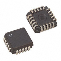
CONNECTION DIAGRAMS
DIL-16, SOIC-16 (TOP VIEW)
J or N Package, DW Package
PLCC-20, LCC-20 (TOP VIEW)
Q, L Packages
PACKAGE PIN FUNCTION
FUNCTION
PIN
N/C
VIN +
−2.0V REF
+1.5V REF
Threshold Adjust
N/C
VIN−
Sense−
Sense+
N.Inv. Input
N/C
Inv. Input
Fault Alert
Fault Delay
Driver Sink
N/C
Driver Source
Compensation/ Shutdown
O.V. Latch Output/Reset
Crowbar Gate
2
1
2
3
4
5
6
7
8
9
10
11
12
13
14
15
16
17
18
19
20
�UC1834
UC2834
UC3834
ELECTRICAL CHARACTERISTICS: Unless otherwise stated, these specifications apply for TA=−55°C to +125°C
for the UC1834, −40°C to +85°C for the UC2834, and 0°C to +70°C for the
UC3834. VIN+ = 15V, VIN− = 0V, TA = TJ.
PARAMETER
Turn-on Characteristics
Standby Supply Current
+1.5 Volt Reference
Output Voltage
Line Regulation
Load Regulation
-2.0 Volt Reference (Note 2)
Output Voltage (Referenced
to VIN+)
Line Regulation
Output Impedance
Error Amplifier Section
Input Offset Voltage
Input Bias Current
Input Offset Current
Small Signal Open Loop Gain
TEST CONDITIONS
UC1834
UC2834
MIN
TYP MAX
5.5
TJ = 25°C
TJ(MIN) ≤ TJ ≤ TJ(MAX)
VIN+ = 5 to 35V
IOUT = 0 to 2mA
1.485
1.47
TJ = 25°C
TJ(MIN) ≤ TJ ≤ TJ(MAX)
VIN+ = 5 to 35V
−2.04
−2.06
1.5
1
1
−2
1.5
2.3
VCM = 1.5V
VCM = 1.5V
VCM = 1.5V
Output @ Pin 14, Pin 12 = VIN+
Pin 13, 20Ω to VIN−
VCM = 0.5 to 33V, VIN+ = 35V
VIN+ = 5 to 35V, VCM = 1.5V
50
1
−1
0.1
65
UC3834
MIN
UNITS
TYP
MAX
5.5
10
mA
1.515 1.47
1.53 1.455
10
10
1.5
1.53
1.545
15
15
V
−1.96 −2.06
−1.94 −2.08
15
−2
7
6
−4
1
50
1
1
1.5
2.3
1
−1
0.1
65
−1.94
−1.92
20
10
−8
2
mV
mV
V
mV
kΩ
mV
µA
µA
dB
60
80
60
80
dB
CMRR
PSRR
70
100
70
100
dB
Driver Section
Maximum Output Current
200
350
200
350
mA
Saturation Voltage
IOUT = 100mA
0.5
1.2
0.5
1.5
V
Output Leakage Current
Pin 12 = 35V, Pin 13 = VIN−, Pin 14 = VIN−
0.1
50
0.1
50
µA
Shutdown Input Voltage
IOUT ≤ 100µA, Pin 13 = VIN−, Pin 12 =
0.4
1
0.4
1
V
at Pin 14
VIN+
−100 −150
−100 −150
µA
Shutdown Input Current
Pin 14 = VIN−, Pin 12 = VIN+
IOUT ≤ 100µA, Pin 13 = VIN−
at Pin 14
Thermal Shutdown (Note 3)
165
165
°C
Fault Amplifier Section
120
150
180
110
150
190
mV
Under- and Over-Voltage
VCM = 1.5V, @ E/A Inputs
Fault Threshold
−0.4 −0.8
−0.4 −1.0
%/v
Common Mode Sensitivity
VIN+ = 35V, VCM = 1.5 to 33V
Supply Sensitivity
VCM = 1.5V, VIN+ = 5 to 35V
−0.5 −1.0
−0.5 −1.2
%/V
Fault Delay
30
45
60
30
45
60 ms/µF
Fault Alert Output Current
2
5
2
5
mA
Fault Alert Saturation Voltage IOUT = 1mA
0.2
0.5
0.2
0.5
V
O.V. Latch Output Current
2
4
2
4
mA
O.V. Latch Saturation Voltage IOUT = 1mA
1.0
1.3
1.0
1.3
V
O.V. Latch Output Reset
0.3
0.4
0.6
0.3
0.4
0.6
V
Voltage
Crowbar Gate Current
−100 −175
−100 −175
mA
Crowbar Gate Leakage
VIN+ = 35V, Pin 16 = VIN−
−0.5
−50
−0.5
−50
µA
Current
Note 2: When using both the 1.5V and −2.0V references the current out of pin 3 should be balanced by an equivalent current into
Pin 2. The −2.0V output will change −2.3mV per µA of imbalance.
Note 3: Thermal shutdown turns off the driver. If Pin 15 (O.V. Latch Output) is tied to Pin 14 (Compensation/Shutdown) the
O.V. Latch will be reset.
3
�UC1834
UC2834
UC3834
ELECTRICAL CHARACTERISTICS: Unless otherwise stated, these specifications apply for TA=−55°C to +125°C
for the UC1834, −40°C to +85°C for the UC2834, and 0°C to +70°C for the
UC3834. VIN+ = 15V, VIN− = 0V. TA = TJ
PARAMETER
TEST CONDITIONS
Current Sense Amplifier Section
Threshold Voltage
Pin 4 Open, VCM = VIN+ or VIN−
Pin 4 = 0.5V, VCM = VIN+ or VIN−
Threshold Supply Sensitivity Pin 4 Open, VCM = VIN−, VIN+ = 5 to 35V
Adj. Input Current
Pin 4 = 0.5V
Sense Input Bias Current
VCM = VIN+
VCM = VIN−
Current Sense Threshold Adjustment
UC1834
UC2834
MIN
TYP MAX
MIN
TYP
MAX
130
40
120
30
150
50
−0.1
−2
100
−100
180
70
−0.5
−10
200
−200
150
50
−0.1
−2
100
−100
170
60
−0.3
−10
200
−200
UC3834
UNITS
Current Limiting Knee Characteristics
Differential Voltage at Current Sense
Inputs - mV (reference to sense − input)
Error Amplifier Gain and Phase
Frequency Response
Current Sense Amplifier Gain and Phase
Frequency Response
4
mV
%/V
µA
µA
�UC1834
UC2834
UC3834
APPLICATION INFORMATION
Foldback Current Limiting
The crowbar output on the UC1834 is activated following a
sustained over-voltage condition. The crowbar output remains
high as long as the fault condition persists, or, as long as the
over-voltage latch is set. The latch is set with an over-voltage
fault if the voltage at Pin 15 is above the latch reset threshold,
typically 0.4V. When the latch is set, its Q− output will pull Pin
15 low through a series diode. As long as a nominal pull-up
load exists, the series diode prevents Q− from pulling Pin 15
below the reset threshold. However, Pin 15 is pulled low
enough to disable the driver outputs if Pins 15 and 14 are
tied together. With Pin 15 and 14 common, the regulator
will latch off in response to an over-voltage fault. If the
fault condition is cleared and Pins 14 and 15 are momentarily pulled below the latch reset threshold, the driver outputs are re-enabled.
Both the current sense and error amplifiers on the UC1834
are transconductance type amplifiers. As a result, their voltage gain is a direct function of the load impedance at their
shared output pin, Pin 14. Their small signal voltage gain as
a function of load and frequency is nominally given by;
ZL (f)
ZL (f)
and AV C. S. ⁄ A =
70Ω
700Ω
for: f ≤ 500kHz and |ZL(f)| ≤ 1 MΩ
Where:
AV=Small Signal Voltage Gain to pin 14.
ZL(f) = Load Impedance at Pin 14.
AV
E⁄A
=
The UC1834 fault delay circuitry prevents the fault outputs
from responding to transient fault conditions. The delay reset
latch insures that the full, user defined, delay passes before an
over-voltage fault response occurs. This prevents unnecessary
crowbar, or latched-off conditions, from occurring following
sharp under-voltage to over-voltage transients.
Setting the Threshold Adjust Voltage (VADJ)
5
�UC1834
UC2834
UC3834
TYPICAL APPLICATIONS
5-10 Amp Positive Regulator
5-10 Amp Negative Regulator
UNITRODE CORPORATION
7 CONTINENTAL BLVD. • MERRIMACK, NH 03054
TEL. (603) 424-2410 • FAX (603) 424-3460
6
�PACKAGE OPTION ADDENDUM
www.ti.com
14-Oct-2022
PACKAGING INFORMATION
Orderable Device
Status
(1)
Package Type Package Pins Package
Drawing
Qty
Eco Plan
(2)
Lead finish/
Ball material
MSL Peak Temp
Op Temp (°C)
Device Marking
(3)
Samples
(4/5)
(6)
5962-87742012A
ACTIVE
LCCC
FK
20
1
Non-RoHS
& Green
SNPB
N / A for Pkg Type
-55 to 125
596287742012A
UC1834L/
883B
5962-8774201EA
ACTIVE
CDIP
J
16
1
Non-RoHS
& Green
SNPB
N / A for Pkg Type
-55 to 125
5962-8774201EA
UC1834J/883B
5962-8774201V2A
ACTIVE
LCCC
FK
20
1
Non-RoHS
& Green
SNPB
N / A for Pkg Type
-55 to 125
59628774201V2A
UC1834L
QMLV
5962-8774201VEA
ACTIVE
CDIP
J
16
1
Non-RoHS
& Green
SNPB
N / A for Pkg Type
-55 to 125
5962-8774201VE
A
UC1834JQMLV
UC1834J
ACTIVE
CDIP
J
16
1
Non-RoHS
& Green
SNPB
N / A for Pkg Type
-55 to 125
UC1834J
Samples
UC1834J883B
ACTIVE
CDIP
J
16
1
Non-RoHS
& Green
SNPB
N / A for Pkg Type
-55 to 125
5962-8774201EA
UC1834J/883B
Samples
UC1834L
ACTIVE
LCCC
FK
20
1
Non-RoHS
& Green
SNPB
N / A for Pkg Type
-55 to 125
UC1834L
Samples
UC1834L883B
ACTIVE
LCCC
FK
20
1
Non-RoHS
& Green
SNPB
N / A for Pkg Type
-55 to 125
596287742012A
UC1834L/
883B
UC2834DW
ACTIVE
SOIC
DW
16
40
RoHS & Green
NIPDAU
Level-2-260C-1 YEAR
-40 to 85
UC2834DW
Samples
UC2834J
ACTIVE
CDIP
J
16
1
Non-RoHS
& Green
SNPB
N / A for Pkg Type
-40 to 85
UC2834J
Samples
UC3834DW
ACTIVE
SOIC
DW
16
40
RoHS & Green
NIPDAU
Level-2-260C-1 YEAR
0 to 70
UC3834DW
Samples
(1)
The marketing status values are defined as follows:
ACTIVE: Product device recommended for new designs.
LIFEBUY: TI has announced that the device will be discontinued, and a lifetime-buy period is in effect.
NRND: Not recommended for new designs. Device is in production to support existing customers, but TI does not recommend using this part in a new design.
PREVIEW: Device has been announced but is not in production. Samples may or may not be available.
OBSOLETE: TI has discontinued the production of the device.
Addendum-Page 1
Samples
Samples
Samples
Samples
Samples
�PACKAGE OPTION ADDENDUM
www.ti.com
14-Oct-2022
(2)
RoHS: TI defines "RoHS" to mean semiconductor products that are compliant with the current EU RoHS requirements for all 10 RoHS substances, including the requirement that RoHS substance
do not exceed 0.1% by weight in homogeneous materials. Where designed to be soldered at high temperatures, "RoHS" products are suitable for use in specified lead-free processes. TI may
reference these types of products as "Pb-Free".
RoHS Exempt: TI defines "RoHS Exempt" to mean products that contain lead but are compliant with EU RoHS pursuant to a specific EU RoHS exemption.
Green: TI defines "Green" to mean the content of Chlorine (Cl) and Bromine (Br) based flame retardants meet JS709B low halogen requirements of


 工商网监
湘ICP备2023018690号
工商网监
湘ICP备2023018690号
