UC3176
UC3177
Full Bridge Power Amplifier
FEATURES
DESCRIPTION
• Dual Power Operational Amplifiers
The UC3176/7 family of full bridge power amplifiers is rated for a continuous output current of 2A. Intended for use in demanding servo applications such as disk head positioning, the onboard current sense amplifier
can be used to obtain precision control of load current, or where voltage
mode drive is required, a standard voltage feedback scheme can be used.
Output stage protection includes foldback current limiting and thermal
shutdown, resulting in a very rugged device.
• ±2A Output Current Guaranteed
• Precision Current Sense Amplifier
• Two Supply Monitoring Inputs
• Parking Function and Under-Voltage
Lockout
• Safe Operating Area Protection
• 3V to 35V Operation
Auxiliary functions on this device include a dual input under-voltage comparator that can be programmed to respond to low voltage conditions on
two independent supplies. In response to an under-voltage condition the
power Op-Amps are inhibited and a high current, 100mA, open collector
drive output is activated. A separate Park/Inhibit command input.
The devices are operational over a 3V to 35V supply range. Internal under-voltage lockout provides predictable power-up and power-down characteristics.
BLOCK DIAGRAM
SLUS285A - OCTOBER 1994 - REVISED JANUARY 2005
�UC3176
UC3177
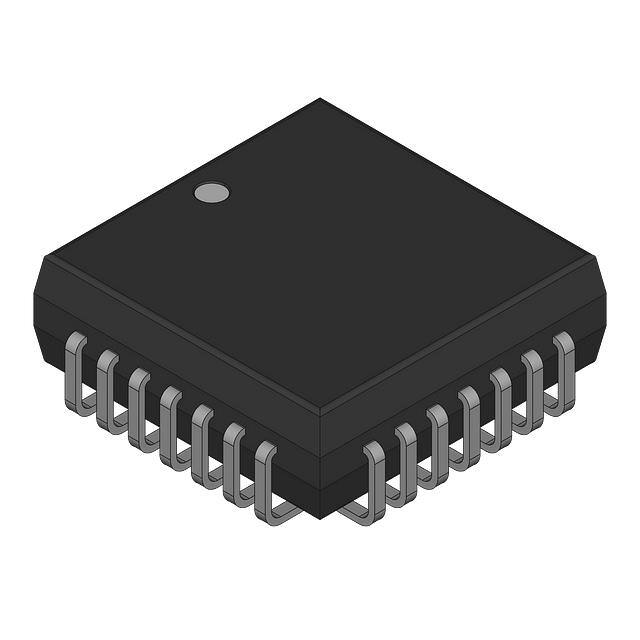
CONNECTION DIAGRAM
ABSOLUTE MAXIMUM RATINGS (Note 1)
Input Supply voltage, (+VIN) . . . . . . . . . . . . . . . . . . . . . . . . 40V
Park/Inhibit, UV1 and UV2 inputs (zener clamped)
Maximum forced voltage . . . . . . . . . . . . . . . . . –0.3V to 10V
Maximum forced current . . . . . . . . . . . . . . . . . . . . . . ±10mA
Other Input Voltages . . . . . . . . . . . . . . . . . . . . . . –0.3V to +VIN
AlSINK and BlSINK Voltages . . . . . . . . . . . . . . . . . . . –0.3V to 6V
Open Collector Output Voltages . . . . . . . . . . . . . . . . . . . . . 40V
A and B Output Currents (Continuous)
Source . . . . . . . . . . . . . . . . . . . . . . . . . . . . Internally Limited
Sink . . . . . . . . . . . . . . . . . . . . . . . . . . . . . . . . . . . . . . . . 2.5A
Total Supply Current (Continuous) . . . . . . . . . . . . . . . . . . . . 4A
Parking Drive Output Current (Continuous) . . . . . . . . . . 200mA
Supply OK Output Current, UC3177 (Continuous) . . . . . . 30mA
Operating Junction Temperature . . . . . . . . . . –55°C to +150°C
Power Dissipation at TC = +75°C
QP package. . . . . . . . . . . . . . . . . . . . . . . . . . . . . . . . . . . 4W
Storage Temperature . . . . . . . . . . . . . . . . . . . –65°C to +150°C
PLCC-28 (Top View)
QP Package
THERMAL DATA
*Pin 9: UC3176, B+ Input
UC3177, Supply OK
QP package:
Thermal Resistance Junction to Leads, θJL . . . . . . . 15°C/W
Thermal Resistance Junction to Ambient, θJA . . . . . 50°C/W
Thermal Resistance Junction to COSC, θJC . . . . . . . 30°C/W
PACKAGE PIN FUNCTION
FUNCTION
PIN
+VIN
B Output
BISINK (Sense)
BISINK
N/C
B– Input
*
Park/Inhibit
Parking Drive
Gnd (Heat Flow Pins)
UV1
UV2
Current Feedback
A+ Input
A– Input
N/C
AISINK
AISINK (Sense)
A Output
Gnd
1
2
3
4
5-7
8
9
10
11
12-18
19
20
21
22
23
24
25
26
27
28
ELECTRICAL CHARACTERISTICS:Unless otherwise stated, specifications hold for TA = 0 to 70°C, +VIN = 12V, TA = TJ.
PARAMETER
TEST CONDITIONS
MIN.
TYP.
MAX. UNITS
Input Supply
Supply Current
UVOL Threshold
+VIN = 12V
18
25
mA
+VIN = 35V
21
30
mA
+VIN low to high
2.8
3.0
V
Threshold Hysteresis
220
300
mV
8
mV
35
µA/V
200
nA
Power, Amplifier, A and B
Input Offset Voltage
VCM = 6V, VOUT = 6V
Input Bias Current
VCM = 6V, Except A+ Input
Input Bias Current at A+/Reference Input
(A+/REF - BISINK) /36kΩ; TJ = 25°C
Input Offset Current B Amp
(UC3176 Only)
VCM = 6V
–500
–100
23
28
nA
CMRR
VCM = 1 to 33V, +VIN = 35V, VOUT = 6V
70
100
dB
PSRR
+VIN = 5 to 35V, VCM = 2.5V
70
100
dB
Large Signal Voltage Gain
VOUT = 3V, w/IOUT = 1A to VOUT = 9V,
w/IOUT = –1A
1.5
4
V/mV
Thermal Feedback
+VIN = 20V, Pd = 20W at opposite output
25
Saturation Voltage
IOUT = –2A, High Side, TJ = 25°
1.9
CIOUT = 2A, Low Side, TJ = 25°C
1.6
Total VSAT at 2A, TJ = 25°C
3.5
200
µV/W
V
V
3.7
V
Unity Gain Bandwidth
1
MHz
Slew Rate
1
V/µs
Differential IOUT Sense Error Current in
Bridge Configuration
High Side Current Limiting
IOUT(A) = –IOUT(B), /IOUT / – /AISINK - BISINK /
IOUT ≤ 200mA
3.0
6.0
mA
IOUT ≤ 2A
5.0
10
mA
=VIN - VOUT < 12V
–2.7
–2.0
A
2
�UC3176
UC3177
ELECTRICAL CHARACTERISTICS:Unless otherwise stated, specifications hold for TA = 0 to 70°C, +VIN = 12V, TA = TJ.
PARAMETER
TEST CONDITIONS
MIN.
TYP.
MAX. UNITS
Current Sense Amplifier
Input Offset Voltage
VCM = 0V, A+ / REF at 6V
REF = 2V to 20V, +VIN = 35, change with REF
Input voltage
Thermal Gradient Sensitivity
+VIN = 20V, REF = 10V Pd = 20W @ A or B
Output
5.0
PSRR
REF = 2.5V, +VIN = 5 to 35V
70
100
Gain
/AISINK-BISINK / ≤ 0.5V
7.8
8.0
Slew Rate
3dB Bandwidth
2.5
3
mV
600
µV/V
75.0
µV/W
dB
8.1
V/V
2
V/µS
1
MHz
MAX Output Current
ISOURCE = +VIN - VOUT = 0.5V
3.5
Output Saturation Voltage
ISOURCE = 1.5mA, High Side
0.15
0.30
mA
V
ISINK = 5mA, Low Side
1.4
1.85
V
1.44
1.50
1.56
V
50
70
80
mV
–2.00
–.05
Under-Voltage Comparator
Threshold Voltage
Low to High, other input at 5V
Threshold Hysteresis
µA
Input Current
Input = 2V, other input at 5V
Supply OK VSAT (UC3177 Only)
IOUT = 5mA
0.45
V
Supply OK Leakage (UC3177 Only)
VOUT = 35V
5
µA
1.3
1.7
V
µA
Park/Inhibit
Park/Inhibit Thl’d
1.1
Park/Inhibit Input Current
At threshold
60
100
Parking Drive Saturation Voltage
IOUT = 100mA
0.3
0.7
V
Parking Drive Leakage
VOUT = 35V
15
µA
Thermal Shutdown
Shutdown Temperature
Output saturation voltage vs. current.
165
Maximum source current vs. + VIN –
VOUT.
3
Crossover current error
characteristic.
°C
�UC3176
UC3177
APPLICATION AND OPERATION INFORMATION
WAVEFORMS FOR ABOVE APPLICATION
DESIGN EQUATIONS
Transconductance (GO) =
IL R F 2 1
=
×
VS R F1 8R S
with: RSA = RSB and RF3 = RF4
Parking Current (IP) =
VIN − 15
.
RP +RL
where: RL = load resistance
Under-Voltage Thresholds, at Supplies
High to Low Threshold, (VLH) = 1.425 (RA + RB)/RB
Low to High Threshold, (VHL) = 1.5 (RA + RB)/RB
4
�PACKAGE OPTION ADDENDUM
www.ti.com
29-Jun-2018
PACKAGING INFORMATION
Orderable Device
Status
(1)
Package Type Package Pins Package
Drawing
Qty
Eco Plan
Lead/Ball Finish
MSL Peak Temp
(2)
(6)
(3)
Op Temp (°C)
Device Marking
(4/5)
UC3176QP
NRND
PLCC
FN
28
37
Green (RoHS
& no Sb/Br)
CU NIPDAU
Level-3-260C-168 HR
0 to 70
UC3176QP
UC3176QPTR
NRND
PLCC
FN
28
750
Green (RoHS
& no Sb/Br)
CU NIPDAU
Level-3-260C-168 HR
0 to 70
UC3176QP
(1)
The marketing status values are defined as follows:
ACTIVE: Product device recommended for new designs.
LIFEBUY: TI has announced that the device will be discontinued, and a lifetime-buy period is in effect.
NRND: Not recommended for new designs. Device is in production to support existing customers, but TI does not recommend using this part in a new design.
PREVIEW: Device has been announced but is not in production. Samples may or may not be available.
OBSOLETE: TI has discontinued the production of the device.
(2)
RoHS: TI defines "RoHS" to mean semiconductor products that are compliant with the current EU RoHS requirements for all 10 RoHS substances, including the requirement that RoHS substance
do not exceed 0.1% by weight in homogeneous materials. Where designed to be soldered at high temperatures, "RoHS" products are suitable for use in specified lead-free processes. TI may
reference these types of products as "Pb-Free".
RoHS Exempt: TI defines "RoHS Exempt" to mean products that contain lead but are compliant with EU RoHS pursuant to a specific EU RoHS exemption.
Green: TI defines "Green" to mean the content of Chlorine (Cl) and Bromine (Br) based flame retardants meet JS709B low halogen requirements of