Not Recommended for New Designs
UC2578
UC3578
application
INFO
available
Buck Pulse Width Modulator Stepdown Voltage Regulator
FEATURES
DESCRIPTION
• Provides Simple Single Inductor Buck
PWM Step-Down Voltage Regulation
The UC3578 is a PWM controller with an integrated high side floating gate
driver. It is used in buck step down converters and regulates a positive
output voltage. Intended to be used in a distributed power system, the IC
allows operation from 14V to 72V input voltage which range includes the
prevalent telecomm bus voltages. The output duty cycle of the UC3578
can vary between 0% and 90% for operation over the wide input voltage
and load conditions.
• Drives External High Side NMOS
Switch
• 14V to 72V Input Voltage Operating
Range
• Contains 100kHz Internal Oscillator,
2V Reference and UVLO
The UC3578 simplifies the design of the single switch PWM buck converter
by incorporating a floating high side driver for an external N-channel
MOSFET switch. It also features a 100kHz fixed frequency oscillator, an
internal 2V precision reference, an error amplifier configured for voltage
mode operation, and a PWM comparator with latching logic. Complementing the traditional voltage mode control block, the UC3578 incorporates an overcurrent shutdown circuit with full cycle soft re-start to limit the
input current to a user defined maximum value during overload operation.
Additional functions include an under voltage lockout circuit to insure that
sufficient input supply voltage is present before any switching activity can
occur.
• Soft Start on Power Up
• Overcurrent Shutdown Followed by
Soft Start
The UC2578 and the UC3578 are both available in surface mount and
thru-hole power packages.
ORDERING INFORMATION
UC2578DP
UC2578N
UC3578DP
UC3578N
TYPICAL APPLICATION DIAGRAM
RSENSE
0.12
15-40 VIN
47µF
RS
1k
RECTIFIER
MBR 3100
15
CGG
1µF
1N4148
0°C to +70°C
PACKAGE
Power SOIC
Power PDIP
Power SOIC
Power PDIP
LOUT
40µH
IRFZ34
CS
1000pF
TEMPERATURE RANGE
–40°C to +85°C
VOUT
1µF
COUT
220µF
5k
10
11
15
10
7
6
DIODE
CS
VGG
OUT
SRC
14 VCC
CCC
1µF
EAINV
2
EAOUT
3
UC3578
16
SS
100k
GND GND GND GND
4
5
12
13
50k
R1
220pF
2200pF
1k
CSS
UDG-99064
05/99
�Not Recommended for New Designs
UC2578
UC3578
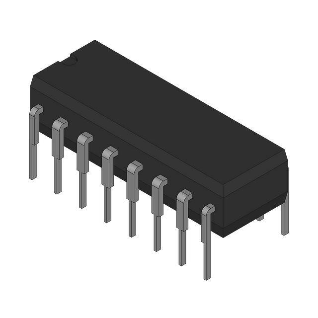
CONNECTION DIAGRAM
ABSOLUTE MAXIMUM RATINGS
VCC . . . . . . . . . . . . . . . . . . . . . . . . . . . . . . . . . . . . . . . . . . +72V
EAINV . . . . . . . . . . . . . . . . . . . . . . . . . . . . . . . . . –0.3V to +10V
EAOUT . . . . . . . . . . . . . . . . . . . . . . . . . . . . . . . . –0.3V to +10V
SS . . . . . . . . . . . . . . . . . . . . . . . . . . . . . . . . . . . . –0.3V to +10V
DIODE . . . . . . . . . . . . . . . . . . . . . . . . . . . . . . . . . –0.3V to VCC
VGG . . . . . . . . . . . . . . . . . . . . . . . . . . . . . . –0.3V to VCC +14V
CS . . . . . . . . . . . . . . . . . . . . . . . . . . . . VCC – 5V to VCC +0.6V
IOUT Pulsed . . . . . . . . . . . . . . . . . . . . . . . . . . . . –0.8A to +0.6A
SRC . . . . . . . . . . . . . . . . . . . . . . . . . . . . . . . . . . . –0.6V to VCC
Storage Temperature . . . . . . . . . . . . . . . . . . . −65°C to +150°C
Junction Temperature . . . . . . . . . . . . . . . . . . . –55°C to +150°C
Lead Temperature (Soldering, 10 sec.) . . . . . . . . . . . . . +300°C
DIL-16, SOIC-16 (Top View)
N or DP Packages
Currents are positive into, negative out of the specified terminal.
Consult Packaging Section of Databook for thermal limitations
and considerations of packages.
Note: The four GND pins are internally connected.
ELECTRICAL CHARACTERISTICS: Unless otherwise specified VCC = 14V, VGG = 14V, TA = TJ.
PARAMETER
TEST CONDITIONS
MIN
TYP
VCC = 14V to 72V, EAINV = 1.9V, TJ = 25°C
100
110
VCC = 11V to 14V, Over Temperature
90
MAX UNITS
Oscillator Section
Frequency
120
kHz
120
kHz
Error Amplifier Section
EAINV
EAOUT = EAINV
IEAINV
EAOUT = EAINV
EAVOL
EAOUT/EAINV, 25°C
70
80
dB
EAOUT High
EAINV ≤ 1.9V, IEAOUT = –100µA
5.5
6.2
V
EAOUT Low
EAINV ≥ 2.1V, IEAOUT = 100µA
Unity Gain Bandwidth
TJ = 25°C, F = 100kHz
PSRR, EAOUT
EAOUT = EAINV, VCC = 14V
1.97
2
2.03
V
100
300
nA
0.8
1.1
V
0.85
1
MHz
80
90
dB
Current Sense Comparator Section
Threshold (Referred to VCC)
0.4
0.5
0.6
V
0.2
1
µA
0.7
1.2
µs
200
300
ns
Input Bias Current
CS = VCC – 0.4V
Propagation Delay
VOVERDRIVE = 250mV
Blanking Time
VOVERDRIVE = 250mV
75
IOUT = –200mA
9.5
11
Gate Drive Output Section
VOH
VOL
V
IOUT = 20mA
0.2
0.36
V
IOUT = 200mA
1.5
2
V
Rise Time
TJ = 25°C, CLOAD = 1nF
40
70
ns
Fall Time
TJ = 25°C, CLOAD = 1nF
40
70
ns
Pulse Width Modulator Section
Maximum Duty Cycle
EAINV ≤ 1.9V
85
90
%
Minimum Duty Cycle
EAINV ≥ 2.1V
0
%
Modulator Gain
EAOUT = 2.5V to 3.5V
30
%/V
Undervoltage Lockout Section
Start Threshold
OUT – SRC, EAINV ≤ 1.9V, SRC = 0V
UVLO Hysteresis
2
10
11
12
V
1.5
2
2.5
V
�Not Recommended for New Designs
UC2578
UC3578
ELECTRICAL CHARACTERISTICS: Unless otherwise specified VCC = 14V, VGG = 14V, TA = TJ.
PARAMETER
TEST CONDITIONS
MIN
TYP
MAX UNITS
VCC = 72V, SRC = 0V, IVGG = –7mA
14.5
15.25
VCC = 50V, SRC = 0V, IVGG = –7mA
14
14.75
16
V
VCC = 15V, SRC = 0V, IVGG = –7mA
13
13.75
14.5
V
VCC = 11V, SRC = 0V, IVGG = –7mA
9.5
10
10.5
V
–30
–45
VGG Regulator Section
VGG – SRC
17
V
Soft Start Ramp Section
Soft Start Ramp Current
µA
Supply Current Section
IVCC
EAINV ≥ 2.1V, SRC = 0V
10
14
mA
IVGG
EAINV ≥ 2.1V, SRC = 0V
7
10.5
mA
PIN DESCRIPTIONS
OUT: Gate drive for the external NMOS switch
connected between VCC and the buck inductor.
CS: Peak current limit sense pin. Senses the current
across a current sense resistor placed between VCC and
the drain of the NMOS buck switch. OUT will be held low
(NMOS buck switch off) if VCC – CS exceeds 0.5V.
SRC: This pin is connected to the junction of the external
NMOS switch source, the floating voltage source
capacitor, the free-wheeling diode cathode, and buck
inductor.
DIODE: An external small signal diode (1N4148 typical)
is connected here, anode to VCC and cathode to
DIODE, to implement the VGG regulator function.
SS: The external soft start capacitor is connected to this
pin.
EAINV: Inverting input to error amplifier. VOUT sense
feedback is connected to this pin. The non-inverting input
of the error amplifier is internally connected to 2V.
VGG: An external capacitor connected from VGG to
SRC completes the floating voltage source for the
floating gate driver. A 1µF capacitor is recommended.
EAOUT: Output of the error amplifier. Use EAOUT and
EAINV for loop compensation components.
VCC: Input supply voltage. This pin supplies an internal
ground referenced voltage regulator that supplies the IC
and an on-chip regulated floating voltage source (VGG –
SRC) used by the floating driver to drive the external
NMOS buck switch. This pin should be bypassed with a
high quality ceramic capacitor.
GND: Circuit Ground. The four ground pins are internally
connected together by the fused leadframe of the
package. They provide the primary thermal conduction
path for dissipating junction heat.
APPLICATION INFORMATION
through a small resistor, as shown in the typical application diagram and in Fig 2. This capacitor provides the energy for the high side driver. The gate drive voltage to
the MOSFET is internally regulated to 14V. A diode
(1N4148) is required from the input voltage to DIODE.
This allows the floating drive capacitor to charge during
conduction of the output rectifier but prevents its discharge back into the supply rail. A 1µF ceramic capacitor
is recommended from VCC to ground to provide high frequency decoupling. Additional decoupling of this pin
could be accomplished by a low value resistor between
VCC and VIN and a 1µF capacitor from VCC to GND as
shown in the schematic.
The UC3578 Floating Buck Controller is a high frequency
switching regulator with a floating driver which provides
PWM control for non-isolated buck converters. The controller operates at a fixed 100 kHz switching frequency,
and in voltage mode control. The duty cycle range of the
PWM output is 0% to 90% allowing for a wide range of
input voltages (14V minimum with transients to 72V).
The regulator features an undervoltage lockout threshold
of 11V with approximately 2V hysterisis as well as soft
start capability. The typical application circuit shown is for
a 15V to 40V input and a 12V at 3A output.
To ensure proper operation of the floating driver, an external capacitor (1µF ceramic) must be connected from
VGG to SRC, and to the source of the external MOSFET
3
�Not Recommended for New Designs
UC2578
UC3578
APPLICATION INFORMATION (cont.)
UDG-97006
Figure 1. Block diagram.
Current Limit
Error Amplifier
The current sense pin provides overcurrent shutdown.
As can be seen from the block diagram, the overcurrent
comparator is wire ANDed with the oscillator after an internally set blanking time. The ILIMIT threshold level is set
by the current sense resistor from RSENSE.
The onboard error amplifier of the UC3578 is a voltage
amplifier with its non-inverting input tied to an internal 2V
reference. As usual, loop compensation can be added
from the inverting input of EAINV to the error amplifier
output at EAOUT. Consideration must be given when
choosing the values of the compensation components
around the amplifier so that the output swing of the amplifier is not restricted. The output of the amplifier can
source 100µA typically.
ILIMIT =
0 .5V
R SENSE
An optional filter can be added (RSCS) from the current
sense resistor to CS to provide high frequency filtering of
the current sense signal if necessary.
General
As in any buck converter, when the switch is off, the
source flies low due to the conduction of the
free-wheeling rectifier. The source (SRC) is pulled below
ground by an amount determined by the forward voltage
drop of the rectifier and by any transient voltage spike
from inductance in this path. The occurrence of this condition could result in erratic operation of the IC during this
period if the negative excursion is not limited. This is because of conduction of current in the substrate of the IC
due to the source pin being pulled below ground and forward biasing the internal substrate PN junction. To limit
this effect, a small resistor (15Ω) can be placed in series
between the MOSFET source and the SRC pin as shown
in Fig. 1. Too large a resistor will limit the drive to the
During a current limit condition, the soft start capacitor on
SS is discharged until its voltage level reaches 1.2V. During this time, a duty cycle clamp is activated to approximately 0.6V above the voltage level on the SS capacitor.
This condition persist until the SS capacitor is discharged
to 1.2V, thus disabling the output driver. At this time, the
SS capacitor is allowed to charge to 5V through the 50µA
current source and normal operation resumes when the
SS capacitor reaches 5V. During the condition described,
the regulator enters a hiccup current limit mode of operation which limits the power dissipation in the MOSFET
and output rectifier under a short circuit condition.
4
�Not Recommended for New Designs
UC2578
UC3578
APPLICATION INFORMATION (cont.)
HS1
IRF530
2
3
30µH
HS2
MBR10100
VIN(+)
VOUT(+)
1
220µF
680pF
1
1
220µF
200
2200µF
2200µF
8.25k
3
0.1µF
0.1µF
330
1N4148
5
VIN(–)
2
51
10
15k
5.62k
VOUT(–)
2
HS3
1
470
TIP47
0.01µF
3
1N4745A
UC3578
47µF
1
N/C
SS 16
2
EAINV
CS 15
3
EAOUT
VCC 14
4
GND
GND 13
5
GND
GND 12
6
SRC
DIODE 11
7
OUT
VGG 10
8
N/C
470pF
2200pF
0.1µF
47k
100pF
N/C
1N4148
9
1µF
HS1, HS2, HS3: HEATSINKS
UDG-99100
Figure 2. Detailed application schematic for the UC3578 evaluation board.
of the thermal management system. Worst case junction-to-ambient thermal resistance for different package
configurations are given in a table in the data book in the
package information section.
MOSFET and result in startup problems with the regulator. A Schottky rectifier is used for the free-wheeling diode to limit the negative excursion of the source. This will
also limit the reverse recovery current thus limiting the inductive voltage spike.
The maximum ambient operating temperature is an important factor in determining what the maximum operating voltage can be for a particular application. For
example, if we assume a maximum operating ambient
temperature of 70°C we can determine what the maximum allowable input voltage can be given other parameters such as package thermal impedance and MOSFET
total gate charge by following the procedure outlined below;
In applications where transient load excursions may result in a no load condition, it is necessary that the output
of the regulator be loaded with a small load current
(10mA to 15mA). This will prevent the output voltage
from going unregulated at no load. This small load current is necessary for proper operation of the floating
driver since the source must fly low to charge up the
floating driver capacitance.
TJ (max) – TA = 125° C – 70° C = 55° C.
Thermal Considerations
For proper operation and reliability of the UC3578,
proper thermal management is essential. It is important
that the designer keep in mind that with surface mount
packages, a significant amount of the heat that the device generates is conducted out through the lead frame.
Because of this, the PCB design becomes a critical part
Pd =
55° C
= 0.95W,
58° C / W
(1)
(2)
where 58°C/W is the worst case theta j-a for the 16 pin
DP package and Pd is the package power dissipation.
5
�Not Recommended for New Designs
UC2578
UC3578
APPLICATION INFORMATION (cont.)
Pd = (Qg • 100kHz + 19mA) • VIN ,
j-a of the package by improving the PCB mounting
method. It is recommended that the four GND pins (4, 5,
12 and 13) be connected to a ground plane to provide a
low resistance thermal path. If a ground plane is not
available, a heat spreader on a double sided PC board is
recommended.
(3)
where Qg is the total MOSFET gate charge and 19mA is
the maximum quiescent current for the UC3578 (ICC +
IGG) from the data sheet. The switching frequency of the
buck converter is 100kHz.
Note: Thermal impedance number is based on device
mounted to 5 square inch FR4 PC board with one ounce
copper. From Unitrode 95-96 data book Table 1, page
9-8, when resistance range is given, lower thermal impedance values are for 5 square inch aluminum PC
board.
The gate charge can be determined from the MOSFET
data sheet. As an example, for a IRFZ34 which has a total gate charge of 46nC, substituting for Pd in equation 3:
0 .95W = (46nC • 100kHz + 19mA) • VIN , and
VIN (max) =
0.95W
= 40V.
0.0236A
ADDITIONAL INFORMATION
Therefore, at 70°C using a IRFZ34 MOSFET the maximum input voltage is limited to 40V to maintain a maximum junction temperature of 125°C in the 16 pin DP
package.
Please refer to the following Unitrode topic for additional
application information.
[1] Application Note U-167, Design and Evaluation of a
48V to 5V Telecom Buck Converter using the UC3578
Control IC by Mark Dennis.
Higher input voltages can be achieved by choosing a
MOSFET with a lower total gate charge or by a reduced
ambient operating temperature or by reducing the theta
30
-55°C
25
-25°C
25°C
ICC (mA)
20
15
125°C
10
85°C
5
0
0
10
20
30
40
VCC (V)
Figure 3. ICC vs. VCC vs. temperature.
UNITRODE CORPORATION
7 CONTINENTAL BLVD. • MERRIMACK, NH 03054
TEL. (603) 424-2410 FAX (603) 424-3460
6
50
60
70
80
�PACKAGE OPTION ADDENDUM
www.ti.com
13-Aug-2021
PACKAGING INFORMATION
Orderable Device
Status
(1)
Package Type Package Pins Package
Drawing
Qty
Eco Plan
(2)
Lead finish/
Ball material
MSL Peak Temp
Op Temp (°C)
Device Marking
(3)
(4/5)
(6)
UC2578DPTR
NRND
SOIC
D
16
2500
RoHS & Green
NIPDAU
Level-2-260C-1 YEAR
-40 to 85
UC2578DP
UC3578DP
NRND
SOIC
D
16
40
RoHS & Green
NIPDAU
Level-2-260C-1 YEAR
0 to 70
UC3578DP
UC3578DPG4
NRND
SOIC
D
16
40
RoHS & Green
NIPDAU
Level-2-260C-1 YEAR
0 to 70
UC3578DP
(1)
The marketing status values are defined as follows:
ACTIVE: Product device recommended for new designs.
LIFEBUY: TI has announced that the device will be discontinued, and a lifetime-buy period is in effect.
NRND: Not recommended for new designs. Device is in production to support existing customers, but TI does not recommend using this part in a new design.
PREVIEW: Device has been announced but is not in production. Samples may or may not be available.
OBSOLETE: TI has discontinued the production of the device.
(2)
RoHS: TI defines "RoHS" to mean semiconductor products that are compliant with the current EU RoHS requirements for all 10 RoHS substances, including the requirement that RoHS substance
do not exceed 0.1% by weight in homogeneous materials. Where designed to be soldered at high temperatures, "RoHS" products are suitable for use in specified lead-free processes. TI may
reference these types of products as "Pb-Free".
RoHS Exempt: TI defines "RoHS Exempt" to mean products that contain lead but are compliant with EU RoHS pursuant to a specific EU RoHS exemption.
Green: TI defines "Green" to mean the content of Chlorine (Cl) and Bromine (Br) based flame retardants meet JS709B low halogen requirements of