UC1637
UC2637
UC3637
Switched Mode Controller for DC Motor Drive
FEATURES
DESCRIPTION
•
Single or Dual Supply
Operation
•
±2.5V to ±20V Input Supply
Range
•
±5% Initial Oscillator
Accuracy; ± 10% Over
Temperature
The UC1637 is a pulse width modulator circuit intended to be used for a variety of
PWM motor drive and amplifier applications requiring either uni-directional or bidirectional drive circuits. When used to replace conventional drivers, this circuit
can increase efficiency and reduce component costs for many applications. All
necessary circuitry is included to generate an analog error signal and modulate
two bi-directional pulse train outputs in proportion to the error signal magnitude
and polarity.
•
Pulse-by-Pulse Current
Limiting
•
Under-Voltage Lockout
This monolithic device contains a sawtooth oscillator, error amplifier, and two
PWM comparators with ±100mA output stages as standard features. Protection
circuitry includes under-voltage lockout, pulse-by-pulse current limiting, and a
shutdown port with a 2.5V temperature compensated threshold.
•
Shutdown Input with
Temperature Compensated
2.5V Threshold
The UC1637 is characterized for operation over the full military temperature range
of -55°C to +125°C, while the UC2637 and UC3637 are characterized for -25°C to
+85°C and 0°C to +70°C, respectively.
•
Uncommitted PWM
Comparators for Design
Flexibility
ABSOLUTE MAXIMUM RATINGS (Note 1)
•
Dual 100mA, Source/Sink
Output Drivers
BLOCK DIAGRAM
6/97
Supply Voltage (±Vs) . . . . . . . . . . . . . . . . . . . . . . . . . . . . . . . . . . . . . . . . . . . . . . . . . . . ±20V
Output Current, Source/Sink (Pins 4, 7) . . . . . . . . . . . . . . . . . . . . . . . . . . . . . . . . . . . 500mA
Analog Inputs (Pins 1, 2, 3, 8, 9, 10, 11 12, 13, 14, 15, 16) . . . . . . . . . . . . . . . . . . . . . . . ±Vs
Error Amplifier Output Current (Pin 17) . . . . . . . . . . . . . . . . . . . . . . . . . . . . . . . . . . . ±20mA
Oscillator Charging Current (Pin 18). . . . . . . . . . . . . . . . . . . . . . . . . . . . . . . . . . . . . . . -2mA
Power Dissipation at TA = 25°C (Note 2) . . . . . . . . . . . . . . . . . . . . . . . . . . . . . . . . 1000mW
Power Dissipation at TC = 25°C (Note 2) . . . . . . . . . . . . . . . . . . . . . . . . . . . . . . . . 2000mW
Storage Temperature Range . . . . . . . . . . . . . . . . . . . . . . . . . . . . . . . . . . . -65°C to +150°C
Lead Temperature (Soldering, 10 Seconds). . . . . . . . . . . . . . . . . . . . . . . . . . . . . . . . +300°C
Note 1: Currents are positive into, negative out of the specified terminal.
Note 2: Consult Packaging Section of Databook for thermal limitations and considerations
of package.
�UC1637
UC2637
UC3637
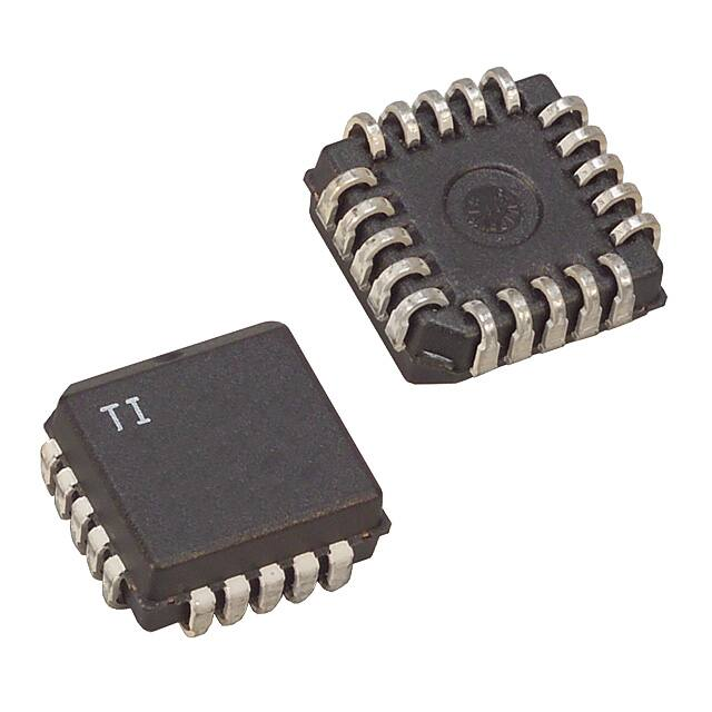
CONNECTION DIAGRAM
PLCC-20, LCC-20
(TOP VIEW)
Q, L Packages
DIL-18 (TOP VIEW)
J or N Package
PACKAGE PIN
FUNCTION
FUNCTION
PIN
+VTH
CT
-VTH
AOUT
-VS
N/C
+VS
BOUT
+BIN
-BIN
-AIN
+AIN
+C/L
-C/L
SHUTDOWN
N/C
+E/A
-E/A
E/A OUTPUT
ISET
SOIC-20 (TOP VIEW)
DW Package
1
2
3
4
5
6
7
8
9
10
11
12
13
14
15
16
17
18
19
20
ELECTRICAL CHARACTERISTICS: Unless otherwise stated, these specifications apply for TA = -55°C to +125°C for the
UC1637; -25°C to +85°C for the UC2637; and 0°C to +70°C for the UC3637; +VS =
+15V, -VS = - 15V, +VTH = 5V, -VTH = -5V, RT = 16.7kΩ, CT = 1500pF, TA=TJ.
PARAMETER
TEST CONDITIONS
UC1637/UC2637
UC3637
UNITS
MIN
TYP
MAX
MIN
TYP
MAX
9.4
10
10.6
9
10
11
kHz
5
7
5
7
%
Oscillator
Initial Accuracy
Voltage Stability
TJ = 25°C (Note 6)
VS = ±5V to ±20V, VPIN 1 = 3V,
VPIN 3 = -3V
Temperature Stability
Over Operating Range (Note 3)
+VTH Input Bias Current
VPIN 2 = 6V
-VTH Input Bias Current
VPIN 2 = 0V
+VTH, -VTH Input Range
0.5
2
-10
0.1
10
-10
-0.5
+VS-2
0.5
2
%
-10
0.1
10
µA
-10
-0.5
-VS+2 +VS-2
µA
-VS+2
V
Error Amplifier
Input Offset Voltage
VCM = 0V
1.5
5
1.5
10
mV
Input Bias Current
VCM = 0V
0.5
5
0.5
5
µA
Input Offset Current
0.1
1
0.1
1
µA
Common Mode Range
VCM = 0V
VS = ±2.5 to 20V
Open Loop Voltage Gain
RL = 10k
-VS+2
75
+VS
100
-VS+2
80
+VS
100
V
dB
Slew Rate
15
15
V/µS
Unity Gain Bandwidth
2
2
MHz
CMRR
PSRR
Over Common Mode Range
VS = ±2.5 to ±20V
2
75
100
75
100
dB
75
110
75
110
dB
�UC1637
UC2637
UC3637
ELECTRICAL CHARACTERISTICS: Unless otherwise stated, these specifications apply for TA = -55°C to +125°C for the
UC1637; -25°C to +85°C for the UC2637; and 0°C to +70°C for the UC3637: VS =
+15V, -VS = - 15V, +VTH = 5V, -VTH = -5V, RT = 16.7kΩ, CT = 1500pF, TA=TJ.
PARAMETERS
TEST CONDITIONS
UC1637/UC2637
MIN
TYP
MAX
-50
-20
UC3637
MIN
UNITS
TYP
MAX
-50
-20
Error Amplifier (Continued)
Output Sink Current
VPIN 17 = 0V
Output Source Current
VPIN 17 = 0V
High Level Output Voltage
mA
5
11
5
11
mA
13
13.6
13
13.6
V
Low Level Output Voltage
-14.8
-13
-14.8
-13
V
PWM Comparators
Input Offset Voltage
VCM = 0V
20
Input Bias Current
VCM = 0V
2
Input Hysteresis
VCM = 0V
VS = ±5V to ±20V
10
Common Mode range
-VS+1
20
10
2
mV
10
10
+VS-2 -VS+1
µA
mV
+VS-2
V
Current Limit
Input Offset Voltage
VCM = 0V, TJ = 25°C
190
Input Offset Voltage T.C.
Input Bias Current
Common Mode Range
200
210
180
-0.2
-10
-1.5
VS = ±2.5V to ±20V
-VS
(Note 4)
-2.3
-2.5
VPIN 14 = +VS to -VS
-10
-0.5
200
220
-0.2
-10
mV
mV/°C
µA
-1.5
+VS-3
-VS
+VS-3
V
-2.7
-2.3
-2.5
-2.7
V
40
mV
-10
-0.5
µA
Shutdown
Shutdown Threshold
Hysteresis
Input Bias Current
40
Under-Voltage Lockout
Start Threshold
(Note 5)
4.15
Hysteresis
5.0
4.15
0.25
5.0
0.25
V
mV
Total Standby Current
Supply Current
8.5
15
8.5
15
mA
-14.9
-13
-14.9
-13
V
-14.5
-13
-14.5
-13
Output Section
Output Low Level
ISINK = 20mA
ISINK = 100mA
Output High Level
ISOURCE = 20mA
13
13.5
ISOURCE = 100mA
12
13.5
Rise Time
(Note 3) CL = Inf, TJ = 25°C
100
600
100
600
ns
Fall Time
(Note 3) CL = Inf, TJ = 25°C
100
300
100
300
ns
Note 3:
Note 4:
Note 5:
Note 6:
13
13.5
12
13.5
V
These parameters, although guaranteed over the recommended operating conditions, are not 100% tested in production.
Parameter measured with respect to +VS (Pin 6).
Parameter measured at +VS (Pin 6) with respect to -VS (Pin 5).
RT and CT referenced to Ground.
FUNCTIONAL DESCRIPTION
Following is a description of each of the functional blocks
shown in the Block Diagram.
minal voltage is buffered internally and also applied to the
lSET terminal to develop the capacitor charging current
through RT. If RT is referenced to -VS as shown in Figure
1, both the threshold voltage and charging current will
vary proportionally to the supply differential, and the oscillator frequency will remain constant. The triangle waveform oscillators frequency and voltage amplitude is
determined by the external components using the formulas
given in Figure 1.
Oscillator
The oscillator consists of two comparators, a charging
and discharging current source, a current source set terminal, lSET and a flip-flop. The upper and lower threshold
of the oscillator waveform is set externally by applying a
voltage at pins +VTH and -VTH respectively. The +VTH ter3
�UC1637
UC2637
UC3637
Figure 1. Oscillator Setup
PWM Comparators
Two comparators are provided to perform pulse width
modulation for each of the output drivers. Inputs are uncommitted to allow maximum flexibility. The pulse width of
the outputs A and B is a function of the sign and amplitude of the error signal. A negative signal at Pin 10 and 8
will lengthen the high state of output A and shorten the
high state of output B. Likewise, a positive error signal reverses the procedure. Typically, the oscillator waveform is
compared against the summation of the error signal and
the level set on Pin 9 and 11.
Figure 2. Comparator Biasing
MODULATION SCHEMES
Case A Zero Deadtime (Equal voltage on Pin 9 and Pin 11)
In this configuration, maximum holding torque or stiffness
and position accuracy is achieved. However, the power input into the motor is increased. Figure 3A shows this configuration.
Output Drivers
Each output driver is capable of both sourcing and sinking
100mA steady state and up to 500mA on a pulsed basis
for rapid switching of either POWERFET or bipolar transistors. Output levels are typically -VS + 0.2V @50mA low
level and +VS - 2.0V @50mA high level.
Case B Small Deadtime (Voltage on Pin 9 > Pin 11)
A small differential voltage between Pin 9 and 11 provides
the necessary time delay to reduce the chances of momentary short circuit in the output stage during transitions, especially where power-amplifiers are used. Refer to
Figure 3B.
Error Amplifier
The error amplifier consists of a high slew rate (15V/µs)
op-amp with a typical 1MHz bandwidth and low output impedance. Depending on the ±VS supply voltage, the common mode input range and the voltage output swing is
within 2V of the VS supply.
Case C Increased Deadtime and Deadband Mode
(Voltage on Pin 9 > Pin 11)
With the reduction of stiffness and position accuracy, the
power input into the motor around the null point of the
servo loop can be reduced or eliminated by widening the
window of the comparator circuit to a degree of acceptance. Where position accuracy and mechanical stiffness
is unimportant, deadband operation can be used. This is
shown in Figure 3C.
Under-Voltage Lockout
An under-voltage lockout circuit holds the outputs in the
low state until a minimum of 4V is reached. At this point,
all internal circuitry is functional and the output drivers are
enabled. If external circuitry requires a higher starting voltage, an over-riding voltage can be programmed through
the shutdown terminal as shown in Figure 4.
4
�UC1637
UC2637
UC3637
Figure 3. Modulation Schemes Showing (A) Zero Deadtime (B) Deadtime and (C) Deadband Configurations
Shutdown Comparator
The shutdown terminal may be used for implementing
various shutdown and protection schemes. By pulling the
terminal more than 2.5V below VIN, the output drivers will
be enabled. This can be realized using an open collector
gate or NPN transistor biased to either ground or the
negative supply. Since the threshold is temperature stabilized, the comparator can be used as an accurate low
voltage lockout (Figure 4) and/or delayed start as in Figure 5. In the shutdown mode the outputs are held in the
low state.
Figure 5. Delayed Start-Up
-VS to within 3V of the +VS supply while providing excellent noise rejection. Figure 6 shows a typical current
sense circuit.
Figure 4. External Under-Voltage Lockout
Current Limit
A latched current limit amplifier with an internal 200mV
offset is provided to allow pulse-by-pulse current limiting.
Differential inputs will accept common mode signals from
Figure 6. Current Limit Sensing
5
�UC1637
UC2637
UC3637
Figure 7. Bi-Directional Motor Drive with Speed Control Power-Amplifier
Figure 8. Single Supply Position Servo Motor Drive
UNITRODE CORPORATION
7 CONTINENTAL BLVD. • MERRIMACK, NH 03054
TEL. (603) 424-2410 • FAX (603) 424-3460
6
�PACKAGE OPTION ADDENDUM
www.ti.com
10-Jun-2022
PACKAGING INFORMATION
Orderable Device
Status
(1)
Package Type Package Pins Package
Drawing
Qty
Eco Plan
(2)
Lead finish/
Ball material
MSL Peak Temp
Op Temp (°C)
Device Marking
(3)
Samples
(4/5)
(6)
5962-89957012A
ACTIVE
LCCC
FK
20
1
Non-RoHS
& Green
SNPB
N / A for Pkg Type
-55 to 125
596289957012A
UC1637L/
883B
5962-8995701VA
ACTIVE
CDIP
J
18
1
Non-RoHS
& Green
SNPB
N / A for Pkg Type
-55 to 125
5962-8995701VA
UC1637J/883B
Samples
UC1637J
ACTIVE
CDIP
J
18
1
Non-RoHS
& Green
SNPB
N / A for Pkg Type
-55 to 125
UC1637J
Samples
UC1637J883B
ACTIVE
CDIP
J
18
1
Non-RoHS
& Green
SNPB
N / A for Pkg Type
-55 to 125
5962-8995701VA
UC1637J/883B
Samples
UC1637L
ACTIVE
LCCC
FK
20
1
Non-RoHS
& Green
SNPB
N / A for Pkg Type
-55 to 125
UC1637L
Samples
UC1637L883B
ACTIVE
LCCC
FK
20
1
Non-RoHS
& Green
SNPB
N / A for Pkg Type
-55 to 125
596289957012A
UC1637L/
883B
UC2637DW
ACTIVE
SOIC
DW
20
25
RoHS & Green
NIPDAU
Level-2-260C-1 YEAR
-25 to 85
UC2637DW
Samples
UC2637DWG4
ACTIVE
SOIC
DW
20
25
RoHS & Green
NIPDAU
Level-2-260C-1 YEAR
-25 to 85
UC2637DW
Samples
UC2637DWTR
ACTIVE
SOIC
DW
20
2000
RoHS & Green
NIPDAU
Level-2-260C-1 YEAR
-25 to 85
UC2637DW
Samples
UC2637J
ACTIVE
CDIP
J
18
1
Non-RoHS
& Green
SNPB
N / A for Pkg Type
0 to 0
UC2637J
Samples
UC2637N
ACTIVE
PDIP
N
18
20
RoHS & Green
NIPDAU
N / A for Pkg Type
-25 to 85
UC2637N
Samples
UC2637NG4
ACTIVE
PDIP
N
18
20
RoHS & Green
NIPDAU
N / A for Pkg Type
-25 to 85
UC2637N
Samples
UC3637DW
ACTIVE
SOIC
DW
20
25
RoHS & Green
NIPDAU
Level-2-260C-1 YEAR
0 to 70
UC3637DW
Samples
UC3637DWTR
ACTIVE
SOIC
DW
20
2000
RoHS & Green
NIPDAU
Level-2-260C-1 YEAR
0 to 70
UC3637DW
Samples
UC3637J
ACTIVE
CDIP
J
18
1
Non-RoHS
& Green
SNPB
N / A for Pkg Type
0 to 70
UC3637J
Samples
UC3637N
ACTIVE
PDIP
N
18
20
RoHS & Green
NIPDAU
N / A for Pkg Type
0 to 70
UC3637N
Samples
Addendum-Page 1
Samples
Samples
�PACKAGE OPTION ADDENDUM
www.ti.com
10-Jun-2022
Orderable Device
Status
(1)
Package Type Package Pins Package
Drawing
Qty
Eco Plan
(2)
Lead finish/
Ball material
RoHS & Green
NIPDAU
MSL Peak Temp
Op Temp (°C)
Device Marking
(3)
Samples
(4/5)
(6)
UC3637NG4
ACTIVE
PDIP
N
18
20
N / A for Pkg Type
0 to 70
UC3637N
(1)
The marketing status values are defined as follows:
ACTIVE: Product device recommended for new designs.
LIFEBUY: TI has announced that the device will be discontinued, and a lifetime-buy period is in effect.
NRND: Not recommended for new designs. Device is in production to support existing customers, but TI does not recommend using this part in a new design.
PREVIEW: Device has been announced but is not in production. Samples may or may not be available.
OBSOLETE: TI has discontinued the production of the device.
(2)
RoHS: TI defines "RoHS" to mean semiconductor products that are compliant with the current EU RoHS requirements for all 10 RoHS substances, including the requirement that RoHS substance
do not exceed 0.1% by weight in homogeneous materials. Where designed to be soldered at high temperatures, "RoHS" products are suitable for use in specified lead-free processes. TI may
reference these types of products as "Pb-Free".
RoHS Exempt: TI defines "RoHS Exempt" to mean products that contain lead but are compliant with EU RoHS pursuant to a specific EU RoHS exemption.
Green: TI defines "Green" to mean the content of Chlorine (Cl) and Bromine (Br) based flame retardants meet JS709B low halogen requirements of