UC1710
UC2710
UC3710
High Current FET Driver
FEATURES
DESCRIPTION
• Totem Pole Output with 6A
Source/Sink Drive
The UC1710 family of FET drivers is made with a high-speed Schottky process to interface between low-level control functions and very high-power
switching devices-particularly power MOSFET’s. These devices accept
low-current digital inputs to activate a high-current, totem pole output which
can source or sink a minimum of 6A.
• 3ns Delay
• 20ns Rise and Fall Time into 2.2nF
• 8ns Rise and Fall Time into 30nF
• 4.7V to 18V Operation
• Inverting and Non-Inverting Outputs
• Under-Voltage Lockout with
Hysteresis
• Thermal Shutdown Protection
Supply voltages for both VIN and VC can independently range from 4.7V to
18V. These devices also feature under-voltage lockout with hysteresis.
The UC1710 is packaged in an 8-pin hermetically sealed dual in-line package for –55°C to +125°C operation. The UC2710 and UC3710 are specified for a temperature range of –40°C to +85°C and 0°C to +70°C
respectively and are available in either an 8-pin plastic dual in-line or a
5-pin, TO-220 package. Surface mount devices are also available.
• MINIDIP and Power Packages
ORDERING INFORMATION
TRUTH TABLE
INV
N.I.
Out
H
H
L
OUT= INV and N.I.
L
H
H
OUT= INV or N.I.
H
L
L
L
L
L
UC1710J
UC2710DW
UC2710J
UC2710N
UC2710T
UC3710DW
UC3710N
UC3710T
TEMPERATURE
RANGE
–55°C to +125°C
–40°C to +85°C
0°C to +70°C
PACKAGE
8 pin CDIP
Not Available
Not Available
8 pin PDIP
5 pin TO220
16 pin SOIC-wide
8 pin PDIP
5 pin TO220
BLOCK DIAGRAM
INTERNALLY CONNECTED IN T PACKAGE
VIN
5
OUTPUT BIAS
4
VC
3
Out
2
Pwr Gnd
LOGIC BIAS
N.I. IN
8
INV IN
1
Logic Gnd
7
TSD
UVLO
INTERNALLY CONNECTED IN T PACKAGE
UDG-99079
05/99
�UC1710
UC2710
UC3710
ABSOLUTE MAXIMUM RATINGS
N-Package
J-Package
T-Package
Supply Voltage, Vin . . . . . . . . . . . . . . . . . . . . . . . . . . . 20V . . . . . . . . . . . . . . 20V . . . . . . . . . . . . . . 20V
Collector Supply Voltage, VC . . . . . . . . . . . . . . . . . . . . 20V . . . . . . . . . . . . . . 20V . . . . . . . . . . . . . . 20V
Operating Voltage . . . . . . . . . . . . . . . . . . . . . . . . . . . . 18V . . . . . . . . . . . . . . 18V . . . . . . . . . . . . . . 18V
Output Current (Source or Sink)
Steady-State. . . . . . . . . . . . . . . . . . . . . . . . . . . . . ± 500mA. . . . . . . . . . . . ± 500mA . . . . . . . . . . . . . ± 1A
Digital Inputs . . . . . . . . . . . . . . . . . . . . . . . . . . . . –0.3V-VIN . . . . . . . . –0.3V – VIN . . . . . . . . –0.3V – VIN
Power Dissipation at Ta=25°C . . . . . . . . . . . . . . . . . . . 1W . . . . . . . . . . . . . . . 1W . . . . . . . . . . . . . . . 3W
Power Dissipation at T (Case) = 25°C. . . . . . . . . . . . . . 2W . . . . . . . . . . . . . . . 2W . . . . . . . . . . . . . . 25W
Operating Junction Temperature . . . . . . . –55°C to +150°C . . . . –55°C to +150°C . . . . –55°C to +150°C
Storage Temperature . . . . . . . . . . . . . . . –65°C to +150°C . . . . –65°C to +150°C . . . . –65°C to +150°C
Lead Temperature (Soldering, 10 seconds) . . . . . . . 300°C . . . . . . . . . . . . 300°C . . . . . . . . . . . . 300°C
Note 1: All currents are positive into, negative out of the specified terminal.
Note 2: Consult Unitrode Integrated Circuits databook for information regarding thermal specifications
and limitations of packages.
CONNECTION DIAGRAMS
DIL-8 MINIDIP (Top View)
J or N Package
SOIC-16 (Top View)
DW Package
5-Pin TO-220 (Top View)
T Package
ELECTRICAL CHARACTERISTICS: Unless otherwise stated, these specifications apply for VIN = VC = 15V, No load,
TA = TJ.
PARAMETERS
VIN Supply Current
VC Supply Current
UVLO Threshold
TEST CONDITIONS
MIN
TYP
MAX UNITS
VIN =18V, VC =18V, Output Low
26
35
mA
VIN =18V, VC =18V, Output High
21
30
mA
VIN =18V, VC =18V, Output Low
1.5
5.0
mA
VIN =18V, VC =18V,Output High
5.0
8
mA
VIN High to Low
3.8
4.1
4.4
V
VIN Low to High
4.1
4.4
4.8
V
2
�UC1710
UC2710
UC3710
ELECTRICAL CHARACTERISTICS: Unless otherwise stated, these specifications apply for VIN = VC = 15V, No load,
TA = TJ.
PARAMETERS
TEST CONDITIONS
UVLO Threshold Hysteresis
MIN
TYP
0.1
0.3
Digital Input Low Level
Digital Input High Level
MAX UNITS
0.5
V
0.8
V
2.0
Digital Input = 0.0V
Output High Sat., VC – VO
IO= –100mA
1.35
2.2
V
IO= –6A
3.2
4.5
V
IO= 100mA
0.25
0.6
V
IO= 6A
3.4
4.5
V
Output Low Sat., VO
Thermal Shutdown
–70
V
Digital Input Current
–4.0
µA
165
°C
From Inv., Input to Output (Note 3, 4):
Rise Time Delay
10% to 90% Rise
Fall Time Delay
90% to 10% Fall
CL = 0
35
70
ns
CL = 2.2nF
35
70
ns
CL = 30nF
35
70
ns
CL = 0
20
40
ns
CL = 2.2nF
25
40
ns
CL = 30nF
85
150
ns
CL = 0
35
70
ns
CL = 2.2nF
35
70
ns
CL = 30nF
35
80
ns
CL = 0
15
40
ns
CL = 2.2nF
20
40
ns
CL = 30nF
85
150
ns
CL = 0
35
70
ns
From N.I. Input to Output (Note 3,4):
Rise Time Delay
10% to 90% Rise
Fall Time Delay
90% to 10% Fall
Total Supply Current at 200kHz Input
Switching Frequency
CL = 2.2nF
35
70
ns
CL = 30nF
35
70
ns
CL = 0
20
40
ns
CL = 2.2nF
25
40
ns
CL = 30nF
85
150
ns
CL = 0
35
70
ns
CL = 2.2nF
35
70
ns
CL = 30nF
35
80
ns
CL = 0
15
40
ns
CL = 2.2nF
20
50
ns
CL = 30nF
85
150
ns
TA = 25°C (Note 5) CL = 0
30
40
mA
Note: 3. Delay measured from 50% input change to 10% output change.
Note: 4. Those parameters with CL = 30nF are not tested in production.
Note: 5. Inv. Input pulsed at 50% duty cycle with N.I. Input = 3V. or N.I. Input pulsed at 50% duty cycle with Inv. Input = 0V.
UNITRODE CORPORATION
7 CONTINENTAL BLVD. • MERRIMACK, NH 03054
TEL. (603) 424-2410 FAX (603) 424-3460
3
�PACKAGE OPTION ADDENDUM
8-Apr-2018
www.ti.com
PACKAGING INFORMATION
Orderable Device
Status
(1)
Package Type Package Pins Package
Drawing
Qty
Eco Plan
Lead/Ball Finish
MSL Peak Temp
(2)
(6)
(3)
Op Temp (°C)
Device Marking
(4/5)
5962-0152001QPA
ACTIVE
CDIP
JG
8
1
TBD
A42
N / A for Pkg Type
-55 to 125
0152001QPA
UC1710
5962-0152001VPA
ACTIVE
CDIP
JG
8
1
TBD
A42
N / A for Pkg Type
-55 to 125
0152001VPA
UC1710
UC1710J
ACTIVE
CDIP
JG
8
1
TBD
A42
N / A for Pkg Type
-55 to 125
UC1710J
UC1710J883B
ACTIVE
CDIP
JG
8
1
TBD
A42
N / A for Pkg Type
-55 to 125
0152001QPA
UC1710
UC2710N
ACTIVE
PDIP
P
8
50
Green (RoHS
& no Sb/Br)
CU NIPDAU
N / A for Pkg Type
-40 to 85
UC2710N
UC2710NG4
ACTIVE
PDIP
P
8
50
Green (RoHS
& no Sb/Br)
CU NIPDAU
N / A for Pkg Type
-40 to 85
UC2710N
UC2710T
ACTIVE
TO-220
KC
5
50
Green (RoHS
& no Sb/Br)
CU SN
N / A for Pkg Type
-40 to 85
UC2710T
UC2710TG3
ACTIVE
TO-220
KC
5
50
Green (RoHS
& no Sb/Br)
CU SN
N / A for Pkg Type
-40 to 85
UC2710T
UC3710DW
ACTIVE
SOIC
DW
16
40
Green (RoHS
& no Sb/Br)
CU NIPDAU
Level-2-260C-1 YEAR
0 to 70
UC3710DW
UC3710DWG4
ACTIVE
SOIC
DW
16
40
Green (RoHS
& no Sb/Br)
CU NIPDAU
Level-2-260C-1 YEAR
0 to 70
UC3710DW
UC3710N
ACTIVE
PDIP
P
8
50
Green (RoHS
& no Sb/Br)
CU NIPDAU | Call TI
N / A for Pkg Type
0 to 70
UC3710N
UC3710NG4
ACTIVE
PDIP
P
8
50
Green (RoHS
& no Sb/Br)
Call TI
N / A for Pkg Type
0 to 70
UC3710N
UC3710T
ACTIVE
TO-220
KC
5
50
Green (RoHS
& no Sb/Br)
CU SN
N / A for Pkg Type
0 to 70
UC3710T
UC3710TG3
ACTIVE
TO-220
KC
5
50
Green (RoHS
& no Sb/Br)
CU SN
N / A for Pkg Type
0 to 70
UC3710T
(1)
The marketing status values are defined as follows:
ACTIVE: Product device recommended for new designs.
LIFEBUY: TI has announced that the device will be discontinued, and a lifetime-buy period is in effect.
NRND: Not recommended for new designs. Device is in production to support existing customers, but TI does not recommend using this part in a new design.
PREVIEW: Device has been announced but is not in production. Samples may or may not be available.
OBSOLETE: TI has discontinued the production of the device.
Addendum-Page 1
Samples
�PACKAGE OPTION ADDENDUM
8-Apr-2018
www.ti.com
(2)
RoHS: TI defines "RoHS" to mean semiconductor products that are compliant with the current EU RoHS requirements for all 10 RoHS substances, including the requirement that RoHS substance
do not exceed 0.1% by weight in homogeneous materials. Where designed to be soldered at high temperatures, "RoHS" products are suitable for use in specified lead-free processes. TI may
reference these types of products as "Pb-Free".
RoHS Exempt: TI defines "RoHS Exempt" to mean products that contain lead but are compliant with EU RoHS pursuant to a specific EU RoHS exemption.
Green: TI defines "Green" to mean the content of Chlorine (Cl) and Bromine (Br) based flame retardants meet JS709B low halogen requirements of
很抱歉,暂时无法提供与“UC3710T”相匹配的价格&库存,您可以联系我们找货
免费人工找货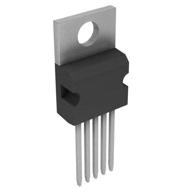


 工商网监
湘ICP备2023018690号
工商网监
湘ICP备2023018690号
