Using the UCC24636EVM
User's Guide
Literature Number: SLUUBE7
March 2016
�www.ti.com
WARNING
Always follow TI’s set-up and application instructions, including use of all interface components within their
recommended electrical rated voltage and power limits. Always use electrical safety precautions to help
ensure your personal safety and the safety of those working around you. Contact TI’s Product Information
Center http://support/ti./com for further information.
Save all warnings and instructions for future reference.
Failure to follow warnings and instructions may result in personal injury, property damage, or
death due to electrical shock and/or burn hazards.
The term TI HV EVM refers to an electronic device typically provided as an open framed, unenclosed
printed circuit board assembly. It is intended strictly for use in development laboratory environments,
solely for qualified professional users having training, expertise, and knowledge of electrical safety risks in
development and application of high-voltage electrical circuits. Any other use and/or application are strictly
prohibited by Texas Instruments. If you are not suitably qualified, you should immediately stop from further
use of the HV EVM.
1. Work Area Safety:
(a) Keep work area clean and orderly.
(b) Qualified observer(s) must be present anytime circuits are energized.
(c) Effective barriers and signage must be present in the area where the TI HV EVM and its interface
electronics are energized, indicating operation of accessible high voltages may be present, for the
purpose of protecting inadvertent access.
(d) All interface circuits, power supplies, evaluation modules, instruments, meters, scopes and other
related apparatus used in a development environment exceeding 50 VRMS/75 VDC must be
electrically located within a protected Emergency Power Off (EPO) protected power strip.
(e) Use a stable and non-conductive work surface.
(f) Use adequately insulated clamps and wires to attach measurement probes and instruments. No
freehand testing whenever possible.
2. Electrical Safety:
(a) De-energize the TI HV EVM and all its inputs, outputs, and electrical loads before performing any
electrical or other diagnostic measurements. Revalidate that TI HV EVM power has been safely deenergized.
(b) With the EVM confirmed de-energized, proceed with required electrical circuit configurations, wiring,
measurement equipment hook-ups and other application needs, while still assuming the EVM circuit
and measuring instruments are electrically live.
(c) Once EVM readiness is complete, energize the EVM as intended.
WARNING: while the EVM is energized, never touch the EVM or its electrical circuits as they
could be at high voltages capable of causing electrical shock hazard.
3. Personal Safety:
(a) Wear personal protective equipment e.g. latex gloves and/or safety glasses with side shields or
protect EVM in an adequate lucent plastic box with interlocks from accidental touch.
4. Limitation for Safe Use:
(a) EVMs are not to be used as all or part of a production unit.
2
SLUUBE7 – March 2016
Submit Documentation Feedback
Copyright © 2016, Texas Instruments Incorporated
�User's Guide
SLUUBE7 – March 2016
Secondary-Side Synchronous Rectifier Controller DiodeReplacement Demonstration Board
1
Introduction
The UCC24636EVM evaluation module (EVM) is used to convert the output rectifier of an off-line
discontinuous mode (DCM) flyback converter from a diode to a MOSFET synchronous rectifier (SR) to
investigate and evaluate the benefits of SR using volt-second balance control. This EVM senses the voltsecond (V-s) product of the transformer magnetization during the primary switch on-time and controls the
on-board SR MOSFET on-time to balance the V-s product during transformer demagnetization. The EVM
is also compatible with transition-mode (TM) operation. SR conduction time can be maximized, regardless
of RDS(on).
The SR-MOSFET can achieve very low conduction loss compared to that of a diode rectifier, significantly
improving efficiency of the converter. Use this EVM to substitute for the diode in an existing DCM or TM
flyback converter to evaluate and optimize the SR performance. It is ideally suited for converters with
output voltages ranging from 5 V to 28 V at current levels up to 5 A, but may be adaptable to other
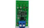
conditions with special considerations. Photographs of the EVM can be seen in Figure 1 and Figure 2.
The UCC24636EVM is not compatible with flyback converters which can operate in continuous conduction
mode (CCM) under any condition. For CCM flyback applications please refer to the UCC24630 SR
controller and its associated UCC24630EVM-636.
Test points on the EVM provide input nodes for VDD bias voltage and ground (GND), VD and VS
connections to the diode anode and cathode nodes, and an output voltage sensing node (VOUT). Two
resistor positions are user programmable to scale the EVM parameters to the specific user application.
These resistor values are calculated based on equations found in the UCC24636 datasheet or by using
the Microsoft Excel®-based UCC24636 Calculator Tool. The UCC24636 controller drives the on-board SR
MOSFET at the correct timing to maximize the SR conduction interval, independently of RDS(on).
The UCC24636EVM works best when substituting for a negative-referenced diode (also known as lowside diode) situated in the return leg of the flyback transformer secondary winding, as shown in Figure 3.
In this arrangement, EVM bias voltage may be obtained directly from the converter output. It is also
possible to use the EVM in a positive-referenced diode position (also known as high-side diode), but this
arrangement requires some additional circuitry to provide bias voltage to the EVM. Figure 25 and
Figure 26 show two methods to implement high-side SR with the EVM. It is not necessary to remove the
diode for which the EVM will substitute; however, a comparison of SR-only losses to diode-only losses will
be compromised.
SLUUBE7 – March 2016
Submit Documentation Feedback
Secondary-Side Synchronous Rectifier Controller Diode-Replacement
Demonstration Board
Copyright © 2016, Texas Instruments Incorporated
3
�Introduction
www.ti.com
Figure 1. Photograph of EVM (Top Side)
Figure 2. Photograph of EVM (Bottom Side)
4
Secondary-Side Synchronous Rectifier Controller Diode-Replacement
Demonstration Board
Copyright © 2016, Texas Instruments Incorporated
SLUUBE7 – March 2016
Submit Documentation Feedback
�Description
www.ti.com
2
Description
This evaluation module uses the TI UCC24636 Synchronous Rectifier Controller With Ultra-Low-Power
Standby Current together with a TI CSD19531Q5A 100-V, 5.3-mΩ MOSFET and various configuration
resistors to implement an SR demonstration board which the user can program to fit a specific application.
This MOSFET can withstand up to 100 V during its off state, and can conduct up to 5 ARMS current without
special cooling. Higher currents may be accommodated, but the additional dissipation by the MOSFET
may raise its case temperature above the safe handling level unless extra cooling is provided.
Seven test points and a terminal block provide access to several important nodes in the SR control circuit.
Refer to the schematic diagram of the UCC24636EVM in Figure 4. In a low-side rectifier application, the
EVM can connect directly to the converter’s output, provided that the output voltage is in the range of 4 V
to 28 V. For high-side rectifier applications, additional biasing circuitry and a special connection
configuration are necessary which are discussed in Section 6.6 and Section 6.7 of this User’s Guide. For
applications where SR is required for converter output voltages lower than the minimum VDD voltage, a
separate source for adequate VDD bias voltage must be provided.
The 2-position terminal block is used to connect the on-board MOSFET source and drain nodes to the
application using user-supplied wires. Short lengths of bare wire, 20 AWG to 18 AWG (0.75 mm to 1 mm
diameter), are best but other sizes with or without insulation can be used. The VDD, GND, and VOUT test
points (TP3, TP4, and TP5, respectively) may be connected to the application using short jumpers with
small spring-clip hooks, or with thinner wires soldered to the test points.
Resistor positions designated R1 and R4 are left unpopulated to allow the user to install those values
which are appropriate to the application. These positions accept surface-mount resistors of 1206 size
(metric 3216) for easier handling. The EVM will not function if resistors R1 and R4 are not properly
populated.
For special applications requiring a different SR MOSFET, an empty DPAK foot-print, designated Q2, is
provided on the back side of the EVM board to accommodate a user-selected device. The 5-mm × 6-mm
SON package, Q1, on the front side should be removed if the back-side Q2 location is populated. In such
a case, take care to ensure that the UCC24636 and other components on the EVM are used within their
parametric limits.
This user’s guide provides the schematic, component list, assembly drawing, art work, and installation
instructions necessary to evaluate the UCC24636 in a typical DCM flyback converter SR application.
IOUT
VBULK
NP
CB1
NS
CB2
VAC
1
VDD HV
TP2
VPC
RS2
3
VS DRV
CBC CS
GND
4
RPL
TP1
VSC
R5
2.2
R1
Set
6
TP5
VOUT
4
DRV
1
5
RLC
RCBC
COUT
Q1
CVDD
2
TP7
VS
UCC24636EVM
7
NA
RS1
J1
TP6
VD
UCC28710
SOIC-7
VAUX
VOUT
VPC
VDD
U1
RCS
R4
Set
UCC24636
R3
10.0k
3
R6
24.3k
TBLK
VSC
GND
5
VBIAS
6
2
R7
49.9k
TP3
VDD
R2
0 C1
1µ
C2
100p
TP4
GND
Figure 3. UCC24636EVM Used in Low-Side Rectifier Application
SLUUBE7 – March 2016
Submit Documentation Feedback
Secondary-Side Synchronous Rectifier Controller Diode-Replacement
Demonstration Board
Copyright © 2016, Texas Instruments Incorporated
5
�Description
2.1
www.ti.com
Applications
The UCC24636 synchronous rectifier controller is suited for use in isolated, off-line, discontinuousconduction-mode (DCM) and transition mode (TM) flyback converters requiring high efficiency and minimal
stand-by power; applications such as:
• USB-Compliant Adapters and Chargers for Consumer Electronics (such as smart phones, tablet
computers, and cameras)
• Stand-By Supply for TV and Desktop
• White Goods
2.2
Features
The UCC24636EVM features include:
• Direct Connection of VDD to Converter Output Voltage Rail, 5 V to 28 V, in Low-Side Applications
• User-Programmable Divider Networks to Adapt the EVM to the Application
• Configured with 5.3-mΩ, 100-V SR MOSFET in SON 5 × 6 Package
• Terminal Block and Test Points for Wiring the SR MOSFET into the Application
• Available TO-252 Solder-Pad on Reverse Side for Alternate MOSFET
CAUTION
High voltage levels may be present on the evaluation module whenever it is
energized, depending on the application in which it is installed. Proper
precautions must be taken when working with the EVM. The voltage on VD test
point TP6 and its associated connection wire may exceed 50 V while operating
in the application. Power to the application must be removed and output voltage
discharged before the EVM can be handled. Serious injury can occur if proper
safety precautions are not followed.
High temperatures may be present on the evaluation module whenever it is
energized, depending on the application in which it is installed. Proper
precautions must be taken when working with the EVM. The temperature of the
MOSFET case and copper heat-sink pad may exceed 50°C while operating in
the application. Power to the application must be removed, output voltage
discharged, and sufficient cool-down time provided before the EVM can be
handled. Serious injury can occur if proper safety precautions are not followed.
6
Secondary-Side Synchronous Rectifier Controller Diode-Replacement
Demonstration Board
Copyright © 2016, Texas Instruments Incorporated
SLUUBE7 – March 2016
Submit Documentation Feedback
�Electrical Performance Specifications
www.ti.com
3
Electrical Performance Specifications
Table 1. UCC24636EVM Electrical Specifications
PARAMETER
CONDITIONS
MIN
TYP
MAX
UNITS
EVM CHARACTERISTICS
VVDD
Bias voltage range
4
5 to 24
28
VDC
VPC voltage range
R1 value calculated for the
application
0.4
2.2
VDC
VSC voltage range
R4 value calculated for the
application
0.3
2.2
VDC
Volt-second product
At VPC input
SR-MOSFET drain voltage
SR-MOSFET on resistance
TJ = 25°C, VDD ≥ 12 V
5.3
7
V-µs
100 (1)
VDC
6.4 (1)
mΩ
5 (1)
ARMS
130 (2)
kHz
SYSTEM CHARACTERISTICS
Maximum SR current
fSW
TA
(1)
(2)
TA = 25°C, TC < 50°C
Switching frequency
Ambient operating temperature
25
ºC
Other voltages, resistances and currents may be accommodated by removing the MOSFET at Q1 and installing a different
MOSFET at Q1 or at Q2, bottom-side.
Based on UCC24636 controller limitation.
SLUUBE7 – March 2016
Submit Documentation Feedback
Secondary-Side Synchronous Rectifier Controller Diode-Replacement
Demonstration Board
Copyright © 2016, Texas Instruments Incorporated
7
�UCC24636EVM Schematic
4
www.ti.com
UCC24636EVM Schematic
The UCC24636EVM schematic diagram indicates two resistor locations (R1 and R4) where the user must
install 1206-size (3216 metric) surface-mount resistors. The values for these resistors are calculated using
the UCC24636 Calculator Tool or from the UCC24636 datasheet equations corresponding to the VPC and
VSC resistor-divider networks. Take care to match the R1 and R4 resistors on the EVM to the
corresponding resistors of the calculator or datasheet, which use different reference designators than
those in Figure 4.
The schematic diagram also indicates a position for an alternative MOSFET, located on the back side of
the EVM board. If the user chooses to modify the EVM and install a MOSFET at Q2, the existing MOSFET
at Q1 should be removed first.
A 0-Ω resistor, R2, connects VDD to VOUT (TP2 to TP3) so that the EVM can be biased by connecting
VDD directly to the converter output voltage. To use this EVM in an application where VOUT may fall
below the UVLO turn-off threshold of the UCC24636 controller, remove R2, connect VDD (TP2) to a
separate bias source, and connect VOUT (TP3) to the converter output.
TP1
VSC
TP2
VPC
VSC
R1
DANGER HIGH VOLTAGE
VPC
VSC
VPC 1
VPC
VDD
VPC Set
DRV
VD
VSC
7,8
5,6,
G
Q1
CSD19531Q5A
100V
VS
TP5
VOUT
6 VDD
R2
4 DRV
VOUT
TBLK
GND
R4
VSC Set
2 VSC
5
VSC
UCC24636DBVR
R5
G
4
2.2
1,2,3
ED120/2DS
GND
0
TBLK 3
VD
1
2
VPC
R3
10.0k
TP6
VD
J1
TP4
GND
U1
VPC
CAUTION HOT SURFACE
TP3
VDD
R6
24.3k
VS
R7
49.9k
C1
1µF
TP7
VS
C2
100pF
GND
DANGER HIGH VOLTAGE
1. R1
User-Selectable Resistor for VPC
1206 (3216) package
VD
G
Q2
2. R4
User-Selectable Resistor for VSC
1206 (3216) package
VS
ALTERNATE MOSFET, N-CH, DPAK
3. UCC24636EVM-001 may be used directly in applications
which limit VD voltage to less than 100V.
Figure 4. UCC24636EVM Schematic Diagram
8
Secondary-Side Synchronous Rectifier Controller Diode-Replacement
Demonstration Board
Copyright © 2016, Texas Instruments Incorporated
SLUUBE7 – March 2016
Submit Documentation Feedback
�Test Setup
www.ti.com
5
Test Setup
Figure 5, Figure 6 and Figure 7 show the method to install the UCC24636EVM into an existing DCM
flyback converter with a diode serving as the output rectifier. In this example, the converter is the
UCC28740EVM-525 rated for 10-W output at 5 V. The output rectifier on this board consists of two
SBR10U45SP5 Schottky diodes connected in parallel for low loss. These diodes are in the high-side
configuration, but the UCC24636EVM is easiest to implement in the low-side configuration. Fortunately,
the flyback transformer uses flying leads on the secondary winding, which allows insertion of the SR into
the low side.
Figure 5 illustrates the top-side view of the UCC28740EVM-525 before modification. It is a straight-forward
modification to disconnect the low-side lead from the converter board and insert the SR EVM in that path,
and apply a short-circuit wire around the high-side diodes. Figure 6 shows the diodes on the bottom side
shorted with wires. Figure 7 shows the UCC24636EVM attached on the top side in the negative leg of the
transformer secondary winding. Figure 8 and Figure 9 show connections to a power source and load, and
voltage and current probing with an oscilloscope. Similar modifications and probing arrangements can be
done to other converters to compare diode versus SR, and to evaluate the converter’s performance with
the UCC24636EVM.
WARNING
High voltages that may cause injury can exist on this evaluation
module (EVM). Please ensure all safety procedures are followed
when working on this EVM. Never leave a powered EVM
unattended.
5.1
Test Equipment
AC Voltage Source: The input source shall be an isolated variable AC source capable of supplying
between 85 VAC and 265 VAC at no less than 20 W and connected as shown in Figure 8 and Figure 9.
Output Load: An isolated programmable electronic or resistive load capable of sinking beyond the
converter output current rating shall be used. For current-limit testing of the converter, an electronic load
should be set to constant resistance mode.
Recommended Wire Gauge: A minimum of 18 AWG (1-mm diameter) wire is recommended for highcurrent connections. The wire lengths between the AC source and the EVM and between the EVM and
the load should not be excessive. Lengths of less than 24 inches (61 cm) long are suggested.
Multimeters: A DC voltmeter should be placed directly across the converter output terminals. A DC
current meter should be placed in series with the converter output after the voltmeter for accurate output
voltage measurements.
Oscilloscope: A high-bandwidth oscilloscope with high-bandwidth probes is recommended.
Fan: Forced-air cooling is not required for low current loads, but for SR current > 5 ARMS additional cooling
should be considered.
Power Analyzer: For accurate efficiency calculations and stand-by power measurements, a high quality
power analyzer should be used; one capable of measuring very low currents. The analyzer’s current
measurement should be inserted in the Neutral or low-voltage path from AC source to the converter.
Measure input power for average efficiency with the analyzer’s voltage inputs across the converter input
terminals. Use the readings from the voltage and current meters on the output to calculate the output
power. To measure stand-by input power, connect the analyzer’s voltage inputs at the AC source output
terminals, and disconnect all other probes and meters from the converter to avoid affecting the
measurement.
SLUUBE7 – March 2016
Submit Documentation Feedback
Secondary-Side Synchronous Rectifier Controller Diode-Replacement
Demonstration Board
Copyright © 2016, Texas Instruments Incorporated
9
�Test Setup
5.2
www.ti.com
Example Test Setup
Figure 5 illustrates the 10-W host converter using high-side output diodes before being retrofitted with the
UCC24636EVM SR module.
Figure 5. UCC28740EVM-525 with Normal Transformer Wiring Before Modification (Top View)
In preparation for installing the SR EVM, the high-side diodes are effectively removed by shorting them out
with short pieces of wire soldered anodes to cathodes.
Figure 6. UCC28740EVM-525 Modified with Schottky Diodes Shorted (Bottom View)
10
Secondary-Side Synchronous Rectifier Controller Diode-Replacement
Demonstration Board
Copyright © 2016, Texas Instruments Incorporated
SLUUBE7 – March 2016
Submit Documentation Feedback
�Test Setup
www.ti.com
Figure 7 shows the SR EVM installed on the top side of the converter EVM with suitable jumper wires at
four locations. Smaller-gauge wires are used to connect VDD and GND (TP3 and TP4) to +VOUT and
–VOUT, respectively, since the bias current to the EVM is low. Thicker wire connects VS and VD at the
terminal block to the converter output ground and low side of the secondary winding, respectively,
because the peak current in this path can be quite high. An additional loop of wire can be added to the VD
path to accommodate a current probe if desired, but the length should be kept as short as possible to
minimize additional leakage inductance. Ensure that the VD wiring connection does not contact the board
or nearby components.
Figure 7. UCC28740EVM-525, Modified with UCC24636EVM Attached
SLUUBE7 – March 2016
Submit Documentation Feedback
Secondary-Side Synchronous Rectifier Controller Diode-Replacement
Demonstration Board
Copyright © 2016, Texas Instruments Incorporated
11
�Test Setup
www.ti.com
Test points TP1 and TP2 (VSC and VPC) are never connected to any external network, but may serve as
observation points for the VSC and VPC signals at the UCC24636 controller. Be careful to avoid injecting
noise into these nodes when probing them. Probe capacitance on the VPC pin may increase the SR turnon delay slightly.
Test point TP5 is used as the input for VOUT from the converter if VDD is sourced from a separate bias
source rather than VOUT of the converter. To use this option, the zero-ohm resistor, R2, connecting TP3
to TP5 on the SR EVM must be removed.
Before the SR EVM is installed, Figure 8 illustrates a low-noise method to probe the output diodes on the
UCC28740EVM-525 board to obtain forward voltage and current waveforms. Since this converter uses
high-side diodes, the diode anode has a widely varying wave-shape, while the cathode is the output
voltage. The oscilloscope probe ground ring should contact a test pin attached to the cathode node, and
the probe tip should contact a test pin on the anode. Since this converter uses an isolation transformer,
the oscilloscope ground effectively ties the output positive node to earth-ground.
WARNING
Do not connect other probe grounds to any other node.
A current probe is clamped around a short loop of wire inserted between the transformer negative flying
lead and the lead’s termination pad. The current probe polarity is oriented to show positive current during
the DCM flyback demagnetization interval.
The diode voltage waveform should be displayed inverted in order to directly compare with the SRMOSFET drain-to-source voltage obtained after the SR EVM is installed.
AC SOURCE
Neutral
Line
OSCILLOSCOPE
LOAD
Figure 8. Method to Measure Diode Voltage and Current on the UCC28740EVM-525
12
Secondary-Side Synchronous Rectifier Controller Diode-Replacement
Demonstration Board
Copyright © 2016, Texas Instruments Incorporated
SLUUBE7 – March 2016
Submit Documentation Feedback
�Test Setup
www.ti.com
After the SR EVM is installed, Figure 9 illustrates a low-noise method to probe the drain-to-source voltage,
VDS, on the UCC24636EVM board to obtain forward voltage waveforms. Since this converter has been
modified to low-side rectification, the drain node has a widely varying waveshape, while the source is the
output ground return. The oscilloscope probe ground ring should contact a test pin attached to the VS
node, and the probe tip should contact a test pin on the VD node. Since this converter uses an isolation
transformer, the oscilloscope ground now effectively ties the output negative node to earth-ground.
A current probe is clamped around a short loop of wire inserted between the transformer negative flying
lead and the SR EVM’s VD input. The current probe polarity is oriented to show positive current during the
DCM flyback demagnetization interval.
The SR VDS waveform should be displayed non-inverted in order to directly compare with the inverted
anode-to-cathode diode voltage obtained before the SR EVM is installed.
AC SOURCE
Neutral
Line
OSCILLOSCOPE
LOAD
Figure 9. Method to Measure SR-MOSFET VDS and Drain Current on UCC28740EVM-525
SLUUBE7 – March 2016
Submit Documentation Feedback
Secondary-Side Synchronous Rectifier Controller Diode-Replacement
Demonstration Board
Copyright © 2016, Texas Instruments Incorporated
13
�Test Setup
5.3
www.ti.com
List of Test Points
Table 2. UCC24636EVM Test Point Functional Description
5.4
TEST POINT
NAME
DESCRIPTION
TP1
VSC
Monitor point for VSC signal, U1 pin 2
TP2
VPC
Monitor point for VPC signal, U1 pin 1
TP3
VDD
SR controller bias supply, U1 pin 6
TP4
GND
SR controller ground, U1 pin 5
TP5
VOUT
Connection for the converter output voltage
TP6
VD
Monitor point for drain of Q1 (also of Q2, if used)
TP7
VS
Monitor point for source of Q1 (also of Q2, if used)
J1-1
VD
Power connection to drain of Q1 (also of Q2, if used)
J1-2
VS
Power connection to source of Q1 (also of Q2, if used)
Applying Power to the Converter EVM
1. Set up the converter EVM as shown in . If testing for efficiency or stand-by power, set up the power
analyzer per the manufacturer’s recommendations.
2. If testing with an electronic load, set it to constant resistance mode.
3. Attach voltmeters, current meters, and oscilloscope probes as necessary to acquire the measurements
desired. For safe operation, do not handle the EVMs after power is applied.
4. Set the AC source voltage to between 85 VAC and 265 VAC.
5. Vary the line and load as desired to evaluate SR operation over the full range of converter operation.
6. Refer to the UCC28740EVM-525 User’s Guide for the power-up and test procedures for evaluation of
the converter’s performance on functional characteristics other than efficiency and stand-by input
power consumption, such as start-up time, transient response, and fault protection, for example.
5.5
Equipment Shutdown
1. To quickly discharge the output capacitors, apply a load greater than 0.1 A on the converter EVM.
2. Turn off the AC source and wait for the primary bulk capacitance to discharge to a safe level before
handling the EVM.
14
Secondary-Side Synchronous Rectifier Controller Diode-Replacement
Demonstration Board
Copyright © 2016, Texas Instruments Incorporated
SLUUBE7 – March 2016
Submit Documentation Feedback
�www.ti.com
6
Waveform Comparisons and Typical Efficiency Curves
Waveform Comparisons and Typical Efficiency Curves
The primary purpose of a synchronous rectifier is to reduce losses compared to that of a diode rectifier
and improve the efficiency of a converter. Various environmental and government agencies world-wide
establish minimum efficiency requirements, with either voluntary or mandatory compliance requirements.
Two notable agency standards are the European Union 2016 Tier-2 Code of Conduct and the United
States Department of Energy 2016 Level-6 targets for minimum average efficiency. Although the
requirements of these two standards are very similar, the Code of Conduct (CoC) is slightly more stringent
and is used for the efficiency and stand-by power targets.
Figure 10 through Figure 13 present the typical current and voltage waveforms associated with the output
rectifier diodes on an unmodified UCC28740EVM-525 board, all measured as shown in Figure 9. These
waveforms correspond to high and low load conditions with low and high input voltages. Figure 14 through
Figure 21 present detailed comparisons between the original diode waveforms and those of the SR when
the UCC24636EVM is installed in place of the diode(s). It can be seen that the current waveforms do not
change noticeably, but the voltage is reduced during the SR conduction time, which reduces losses and
increases efficiency.
After the waveform comparison sections, efficiency and stand-by power loss measurements are compared
in Figure 22 through Figure 24, to show the typical differences obtained when using an SR controlled by
the UCC24636.
Other switching waveforms and system performance characteristics of the flyback converter are covered
by the UCC28740EVM-525 User’s Guide and are not repeated here.
SLUUBE7 – March 2016
Submit Documentation Feedback
Secondary-Side Synchronous Rectifier Controller Diode-Replacement
Demonstration Board
Copyright © 2016, Texas Instruments Incorporated
15
�Waveform Comparisons and Typical Efficiency Curves
6.1
www.ti.com
Full-Load and Light-Load Waveforms of Converter with Output Diode at 85 VAC and
265 VAC
Figure 10 through Figure 13 show the switching waveforms associated with the output diodes on an
unmodified converter UCC28740EVM-525 when operating near the extremes of the rated line and load
conditions. All four figures have waveforms scaled to the same settings and time sweep for easy
comparison. As can be seen, the current through the diode(s) does not change significantly when the
input voltage is varied. However, the voltage stress on the diode (and consequently, on an SR-MOSFET)
increases significantly as the input line voltage is raised from 85 VAC to 265 VAC. The same design
considerations to limit peak voltage stress and dampen ringing on diodes apply to SR-MOSFETs as well.
16
Figure 10. 100%-Load Diode Current and Voltage on
UCC28740EVM-525 at 85-VAC Input
Figure 11. 100%-Load Diode Current and Voltage on
UCC28740EVM-525 at 265-VAC Input
Figure 12. 1%-Load Diode Current and Voltage on
UCC28740EVM-525 at 85-VAC Input
Figure 13. 1%-Load Diode Current and Voltage on
UCC28740EVM-525 at 265-VAC Input
Secondary-Side Synchronous Rectifier Controller Diode-Replacement
Demonstration Board
Copyright © 2016, Texas Instruments Incorporated
SLUUBE7 – March 2016
Submit Documentation Feedback
�Waveform Comparisons and Typical Efficiency Curves
www.ti.com
6.2
Detailed Comparison of Diode to SR Waveforms at 85-VAC and 265-VAC Inputs, 5.0-V
2.0-A Output
Figure 14 through Figure 17 use a faster time scale (1 µs/div) and expanded voltage scale (1 V/div) to
emphasize the difference in power loss of the output rectifier. The secondary winding current (scaled at 2
A/div) drops linearly to zero from a peak of about 10 A (neglecting the ringing), as is characteristic of a
DCM flyback converter. The forward voltage drop of the parallel diodes in Figure 14 and Figure 16
averages about 0.4 V during the diode conduction time. By contrast, the drain-to-source voltage of the SRMOSFET in Figure 15 and Figure 17 is less than 0.1 V over most of the same interval. Notable exceptions
are at the peak of the current and near the zero-crossing of the current. Peak current flows momentarily
(about 100 ns) through the body-diode of the SR-MOSFET before the UCC24636 detects the negative SR
voltage and turns on the MOSFET. Residual current also flows through the body-diode when the MOSFET
is turned off prior to the current reaching zero. The durations of body-diode conduction at the beginning
and end of the SR conduction interval may be different in each application and depend on the impedances
at the controller’s VPC and VSC inputs.
Figure 14. Diode Current and Voltage on UCC28740EVM525 at 85-VAC Input
Figure 15. SR Current and Voltage on UCC28740EVM-525
at 85-VAC Input
Figure 16. Diode Current and Voltage on UCC28740EVM525 at 265-VAC Input
Figure 17. SR Current and Voltage on UCC28740EVM-525
at 265-VAC Input
SLUUBE7 – March 2016
Submit Documentation Feedback
Secondary-Side Synchronous Rectifier Controller Diode-Replacement
Demonstration Board
Copyright © 2016, Texas Instruments Incorporated
17
�Waveform Comparisons and Typical Efficiency Curves
6.3
www.ti.com
Comparison of Diode to SR Waveforms at 85-VAC and 265-VAC Inputs, 5.0-V / 0.02-A
Output
Figure 18 through Figure 21 illustrate the same waveforms characteristics as those of Figure 14 through
Figure 17, except at a very light load (20 mA) on the output. The time scale has been increased to 400
ns/div to show more of the waveforms across the oscilloscope display. The secondary winding current
now peaks at about 3 A but still drops linearly to zero. The forward voltage drop of the parallel diodes in
Figure 18 and Figure 20 averages about 0.3 V during the diode conduction time. By contrast, the drain-tosource voltage of the SR-MOSFET in Figure 19 and Figure 21 is too low to measure over most of the
same interval. The SR conduction voltage may be estimated using the RDS(on) rating of the MOSFET.
Again, exceptions are at the peak of the current and near the zero-crossing of the current, where the SRMOSFET is not turned on. The durations of body-diode conduction at the beginning and end of the SR
conduction interval may be different in each application and depend on the impedances at the controller’s
VPC and VSC inputs.
18
Figure 18. Diode Current and Voltage on UCC28740EVM525 at 85-VAC Input
Figure 19. SR Current and Voltage on UCC28740EVM-525
at 85-VAC Input
Figure 20. Diode Current and Voltage on UCC28740EVM525 at 265-VAC Input
Figure 21. SR Current and Voltage on UCC28740EVM-525
at 265-VAC Input
Secondary-Side Synchronous Rectifier Controller Diode-Replacement
Demonstration Board
Copyright © 2016, Texas Instruments Incorporated
SLUUBE7 – March 2016
Submit Documentation Feedback
�Waveform Comparisons and Typical Efficiency Curves
www.ti.com
6.4
Comparison of Average Efficiency with Diode vs. SR
The average efficiency at 230 VAC, 50 Hz exceeds the 0.79 design goal established to meet the 2016
Code of Conduct average efficiency target for low voltage outputs at a 10-W rating. The average efficiency
at 115 VAC, 60 Hz exceeds the 0.787 design goal established to meet the 2016 DoE Level-6 average
efficiency requirement for low voltage EPS outputs at a 10-W rating. Figure 22 shows the actual measured
efficiency with respect to load current.
10-W Board Efficiency with Diode or SR in Output
85
83
81
% Efficiency
79
77
75
73
71
230 VAC, 50 Hz, SR
115 VAC, 60 Hz, SR
230 VAC, 50 Hz, Diode
115 VAC, 60 Hz, Diode
CoC-2016-Avg
CoC-2016-10%
69
67
65
0.0
0.5
1.0
Output Current (A)
1.5
2.0
2.3
D001
Figure 22. Comparison of UCC28740EVM-525 Efficiency Using SR vs. Diodes
Figure 23 highlights the overall efficiency improvement of the SR over that of parallel diodes.
Notably, there appears to be considerable loss of efficiency with SR at loads less 0.2 A (in this case, loads
less than 10% of rated output). This is a mathematical result of the additional power needed to operate the
SR circuit compared to the low power being delivered to the output. When load falls low enough to reduce
the converter’s average switching frequency to less than approximately 5 kHz, the UCC24636 operation
goes into a stand-by mode to minimize stand-by power and the SR-MOSFET rectifies by body-diode
conduction.
10-W Board Efficiency Improvement with SR in Output
4
3
% Efficiency Improvement
2
1
0
-1
-2
-3
-4
-5
230 VAC, 50 Hz, SR Gain
115 VAC, 60 Hz, SR gain
-6
0
0.5
1
Output Current (A)
1.5
2
2.3
D002
Figure 23. Improvement in Overall Efficiency with UCC24636EVM SR Installed
SLUUBE7 – March 2016
Submit Documentation Feedback
Secondary-Side Synchronous Rectifier Controller Diode-Replacement
Demonstration Board
Copyright © 2016, Texas Instruments Incorporated
19
�Waveform Comparisons and Typical Efficiency Curves
6.5
www.ti.com
Comparison of No-Load Input Power Consumption with Diode vs. SR
Using the UCC24636EVM to implement SR increases the converter no-load input power consumption by
less than 3 mW over the entire input line range.
PSTBY with Diodes and with UCC24636EVM SR
18
No-Load Stand-by Input Power (mW)
16
UCC24636EVM SR
SBR10U45SP5 Diodes
Increase due to SR
14
12
10
8
6
4
2
0
85
115
145
175
Input Line Voltage (VRMS)
205
235
265
D003
Figure 24. Comparison of No-Load Input Power Consumption
20
Secondary-Side Synchronous Rectifier Controller Diode-Replacement
Demonstration Board
Copyright © 2016, Texas Instruments Incorporated
SLUUBE7 – March 2016
Submit Documentation Feedback
�Waveform Comparisons and Typical Efficiency Curves
www.ti.com
6.6
High-Side Diode Replacement with Bias Winding
Figure 25 shows the preferred method to implement a high-side SR application. A separate bias winding,
NB, provides power to VDD and reflects the output voltage to the VSC input divider network. Ideally, the
turns-ratio of NB to NS would be 1:1 so that VDD tracks VOUT, but this is not a strict requirement. If the
output voltage is too low, such that NB must have more turns to generate a higher VDD, the VSC divider
network must compensate for the difference in voltage so that VSC tracks VOUT as if the SR was in a lowside application.
The ground reference of the UCC24636EVM becomes a floating virtual ground, riding on the NS
secondary waveform. In this way, the pulsing voltage presented to the VPC input is recreated.
A standard-recovery diode (not fast or ultra-fast diode) used on the NB winding helps to avoid peakcharging of VDD from leakage inductance effects.
Because the floating bias winding arrangement may be susceptible to noise injection into the VPC and
VSC inputs, filter capacitors may be required to reject the noise. A relatively large value of capacitance
may be applied to VSC, since VSC is proportional to VOUT which is normally regulated. However, it should
not be so large that it prevents VSC from closely tracking changes in VOUT. Only a few picofarads of
capacitance are appropriate to filter VPC. The SR-MOSFET is turned on when the voltage at VPC goes
negative, and an excessive time constant on VPC will delay SR turn-on. Delayed turn-on results in higher
losses and lower efficiency than expected.
NB
RB
IOUT
VBULK
NP
CB1
CB2
VAC
1
VDD HV
7
RS2
RTL
COUT
Q1
TP1
VSC
CVDD
VS DRV
6
CS
CBC
3
GND
5
2
TP6
VD
UCC24636EVM
NA
RS1
J1
TP7
VS
UCC28740
SOIC-7
VAUX
VOUT
NS
TP3
VDD
RLC
RCS
TP5
VOUT
TP4
GND
RFB1
R1
Set
4
ZFB
DRV
VBIAS
6
R2
C1 0
1µ
4
TP2
VPC
R5
2.2
C2
100p
VPC
1
RFB2
UCC24636
2
R7
49.9k
VDD
U1
R4
Set
VSC
TBLK
GND
5
R3
10.0k
3
R6
24.3k
Figure 25. UCC24636EVM Used in the High-Side Rectifier Configuration
SLUUBE7 – March 2016
Submit Documentation Feedback
Secondary-Side Synchronous Rectifier Controller Diode-Replacement
Demonstration Board
Copyright © 2016, Texas Instruments Incorporated
21
�Waveform Comparisons and Typical Efficiency Curves
6.7
www.ti.com
High-Side Diode Replacement without Bias Winding
Figure 26 shows an alternative method to implement a high-side SR application that does not require a
separate bias winding. A major drawback to this method is that VSC does not track VOUT. The
UCC24636EVM operates on a floating virtual ground, again riding on the secondary winding voltage.
Charge-pump action provides power to VDD, but this voltage varies with the primary-side bulk voltage.
VDD does not track VOUT and so the VSC input must be programmed from a fixed reference voltage
corresponding to the highest value of VOUT.
Because VSC cannot track VOUT, there must be a compromise on SR timing to allow for VOUT variations.
The fixed reference voltage for VSC must accommodate the highest VOUT. Consequently, the SR on-time
becomes shorter when VOUT becomes lower. The shorter on-time may result in higher losses and lower
efficiency than expected.
In this implementation, just as in the previous case of Figure 25, the ground reference of the
UCC24636EVM becomes a floating virtual ground, riding on the NS secondary waveform. In this way, the
pulsing voltage presented to the VPC input is recreated.
The drawbacks of this specific high-side SR configuration should be thoroughly considered before
committing to its implementation, to ensure that the application is compatible with its limitations.
IOUT
VBULK
NP
CB1
NS
CB2
VAC
1
VDD HV
RPL
TP1
VSC
VS DRV
6
CS
5
TP3
VDD
RS2
CBC
3
GND
RCBC
COUT
Q1
7
CVDD
2
TP6
VD
UCC24636EVM
NA
RS1
J1
TP7
VS
UCC28710
SOIC-7
VAUX
VOUT
RLC
TP5
VOUT
RCS
6
VPC
1
UCC24636
2
C2
100p
VDD
U1
R4
Set
1µ
TP4
GND
R1
Set
4
DRV
VBIAS
R2
Removed
R2
C1 0
4
TP2
VPC
R5
2.2
R7
49.9k
VSC
TBLK
GND
5
R3
10.0k
3
R6
24.3k
Figure 26. UCC24636EVM Used in the Alternate High-Side Rectifier Configuration
22
Secondary-Side Synchronous Rectifier Controller Diode-Replacement
Demonstration Board
Copyright © 2016, Texas Instruments Incorporated
SLUUBE7 – March 2016
Submit Documentation Feedback
�Assembly Drawing/Layout
www.ti.com
7
Assembly Drawing/Layout
Figure 27 and Figure 28 show the design of the UCC24636EVM printed circuit board. The final
dimensions of the 2-layer circuit board measure 1.70 inches (43.2 mm) long by 0.82 inches (20.8 mm)
wide.
Figure 27. UCC24636EVM Assembly and Copper Drawings (Top View)
Figure 28. UCC24636EVM Assembly and Copper Drawings (Bottom View)
SLUUBE7 – March 2016
Submit Documentation Feedback
Secondary-Side Synchronous Rectifier Controller Diode-Replacement
Demonstration Board
Copyright © 2016, Texas Instruments Incorporated
23
�List of Materials
8
www.ti.com
List of Materials
Table 3 EVM components list, corresponding to the schematic diagram of Figure 4.
Table 3. UCC24636EVM List of Materials
QTY
DESCRIPTION
PART NUMBER
MANUFACTURER
PCB1
Printed circuit board
SV601268
Any
1
C1
Capacitor, ceramic, 1 µF, 50 V, ±10%, X7R, 0805
08055C105KAT2A
AVX
1
C2
Capacitor, ceramic, 100 pF, 50 V, ±5%, C0G/NP0, 0603
06035A101JAT2A
AVX
1
Q1
MOSFET, N-channel, 100 V, 16 A, SON 5 mm × 6 mm
CSD19531Q5A
Texas Instruments
1
R2
Resistor, 0 Ω, 5%, 0.1 W, 0603
CRCW06030000Z0EA
Vishay-Dale
1
R3
Resistor, 10.0 kΩ, 1%, 0.1 W, 0603
CRCW060310K0FKEA
Vishay-Dale
1
R5
Resistor, 2.2 Ω, 5%, 0.1 W, 0603
CRCW06032R20JNEA
Vishay-Dale
1
R6
Resistor, 24.3 kΩ, 1%, 0.1 W, 0603
CRCW060324K3FKEA
Vishay-Dale
1
R7
Resistor, 49.9 kΩ, 1%, 0.1 W, 0603
CRCW060349K9FKEA
Vishay-Dale
3
TP1, TP2,
Test point, miniature, white, TH
TP5
5002
Keystone
1
TP3
Test point, miniature, red, TH
5000
Keystone
1
TP4
Test point, miniature, black, TH
5001
Keystone
1
TP6
Test point, miniature, orange, TH
5003
Keystone
1
TP7
Test point, miniature, yellow, TH
5004
Keystone
U1
Synchronous Rectifier Controller with Low Power
Standby, DBV0006A
UCC24636DBVR
Texas Instruments
1
24
DES
1
Secondary-Side Synchronous Rectifier Controller Diode-Replacement
Demonstration Board
Copyright © 2016, Texas Instruments Incorporated
SLUUBE7 – March 2016
Submit Documentation Feedback
�STANDARD TERMS AND CONDITIONS FOR EVALUATION MODULES
1.
Delivery: TI delivers TI evaluation boards, kits, or modules, including any accompanying demonstration software, components, or
documentation (collectively, an “EVM” or “EVMs”) to the User (“User”) in accordance with the terms and conditions set forth herein.
Acceptance of the EVM is expressly subject to the following terms and conditions.
1.1 EVMs are intended solely for product or software developers for use in a research and development setting to facilitate feasibility
evaluation, experimentation, or scientific analysis of TI semiconductors products. EVMs have no direct function and are not
finished products. EVMs shall not be directly or indirectly assembled as a part or subassembly in any finished product. For
clarification, any software or software tools provided with the EVM (“Software”) shall not be subject to the terms and conditions
set forth herein but rather shall be subject to the applicable terms and conditions that accompany such Software
1.2 EVMs are not intended for consumer or household use. EVMs may not be sold, sublicensed, leased, rented, loaned, assigned,
or otherwise distributed for commercial purposes by Users, in whole or in part, or used in any finished product or production
system.
2
Limited Warranty and Related Remedies/Disclaimers:
2.1 These terms and conditions do not apply to Software. The warranty, if any, for Software is covered in the applicable Software
License Agreement.
2.2 TI warrants that the TI EVM will conform to TI's published specifications for ninety (90) days after the date TI delivers such EVM
to User. Notwithstanding the foregoing, TI shall not be liable for any defects that are caused by neglect, misuse or mistreatment
by an entity other than TI, including improper installation or testing, or for any EVMs that have been altered or modified in any
way by an entity other than TI. Moreover, TI shall not be liable for any defects that result from User's design, specifications or
instructions for such EVMs. Testing and other quality control techniques are used to the extent TI deems necessary or as
mandated by government requirements. TI does not test all parameters of each EVM.
2.3 If any EVM fails to conform to the warranty set forth above, TI's sole liability shall be at its option to repair or replace such EVM,
or credit User's account for such EVM. TI's liability under this warranty shall be limited to EVMs that are returned during the
warranty period to the address designated by TI and that are determined by TI not to conform to such warranty. If TI elects to
repair or replace such EVM, TI shall have a reasonable time to repair such EVM or provide replacements. Repaired EVMs shall
be warranted for the remainder of the original warranty period. Replaced EVMs shall be warranted for a new full ninety (90) day
warranty period.
3
Regulatory Notices:
3.1 United States
3.1.1
Notice applicable to EVMs not FCC-Approved:
This kit is designed to allow product developers to evaluate electronic components, circuitry, or software associated with the kit
to determine whether to incorporate such items in a finished product and software developers to write software applications for
use with the end product. This kit is not a finished product and when assembled may not be resold or otherwise marketed unless
all required FCC equipment authorizations are first obtained. Operation is subject to the condition that this product not cause
harmful interference to licensed radio stations and that this product accept harmful interference. Unless the assembled kit is
designed to operate under part 15, part 18 or part 95 of this chapter, the operator of the kit must operate under the authority of
an FCC license holder or must secure an experimental authorization under part 5 of this chapter.
3.1.2
For EVMs annotated as FCC – FEDERAL COMMUNICATIONS COMMISSION Part 15 Compliant:
CAUTION
This device complies with part 15 of the FCC Rules. Operation is subject to the following two conditions: (1) This device may not
cause harmful interference, and (2) this device must accept any interference received, including interference that may cause
undesired operation.
Changes or modifications not expressly approved by the party responsible for compliance could void the user's authority to
operate the equipment.
FCC Interference Statement for Class A EVM devices
NOTE: This equipment has been tested and found to comply with the limits for a Class A digital device, pursuant to part 15 of
the FCC Rules. These limits are designed to provide reasonable protection against harmful interference when the equipment is
operated in a commercial environment. This equipment generates, uses, and can radiate radio frequency energy and, if not
installed and used in accordance with the instruction manual, may cause harmful interference to radio communications.
Operation of this equipment in a residential area is likely to cause harmful interference in which case the user will be required to
correct the interference at his own expense.
SPACER
SPACER
SPACER
SPACER
SPACER
SPACER
SPACER
SPACER
�FCC Interference Statement for Class B EVM devices
NOTE: This equipment has been tested and found to comply with the limits for a Class B digital device, pursuant to part 15 of
the FCC Rules. These limits are designed to provide reasonable protection against harmful interference in a residential
installation. This equipment generates, uses and can radiate radio frequency energy and, if not installed and used in accordance
with the instructions, may cause harmful interference to radio communications. However, there is no guarantee that interference
will not occur in a particular installation. If this equipment does cause harmful interference to radio or television reception, which
can be determined by turning the equipment off and on, the user is encouraged to try to correct the interference by one or more
of the following measures:
•
•
•
•
Reorient or relocate the receiving antenna.
Increase the separation between the equipment and receiver.
Connect the equipment into an outlet on a circuit different from that to which the receiver is connected.
Consult the dealer or an experienced radio/TV technician for help.
3.2 Canada
3.2.1
For EVMs issued with an Industry Canada Certificate of Conformance to RSS-210
Concerning EVMs Including Radio Transmitters:
This device complies with Industry Canada license-exempt RSS standard(s). Operation is subject to the following two conditions:
(1) this device may not cause interference, and (2) this device must accept any interference, including interference that may
cause undesired operation of the device.
Concernant les EVMs avec appareils radio:
Le présent appareil est conforme aux CNR d'Industrie Canada applicables aux appareils radio exempts de licence. L'exploitation
est autorisée aux deux conditions suivantes: (1) l'appareil ne doit pas produire de brouillage, et (2) l'utilisateur de l'appareil doit
accepter tout brouillage radioélectrique subi, même si le brouillage est susceptible d'en compromettre le fonctionnement.
Concerning EVMs Including Detachable Antennas:
Under Industry Canada regulations, this radio transmitter may only operate using an antenna of a type and maximum (or lesser)
gain approved for the transmitter by Industry Canada. To reduce potential radio interference to other users, the antenna type
and its gain should be so chosen that the equivalent isotropically radiated power (e.i.r.p.) is not more than that necessary for
successful communication. This radio transmitter has been approved by Industry Canada to operate with the antenna types
listed in the user guide with the maximum permissible gain and required antenna impedance for each antenna type indicated.
Antenna types not included in this list, having a gain greater than the maximum gain indicated for that type, are strictly prohibited
for use with this device.
Concernant les EVMs avec antennes détachables
Conformément à la réglementation d'Industrie Canada, le présent émetteur radio peut fonctionner avec une antenne d'un type et
d'un gain maximal (ou inférieur) approuvé pour l'émetteur par Industrie Canada. Dans le but de réduire les risques de brouillage
radioélectrique à l'intention des autres utilisateurs, il faut choisir le type d'antenne et son gain de sorte que la puissance isotrope
rayonnée équivalente (p.i.r.e.) ne dépasse pas l'intensité nécessaire à l'établissement d'une communication satisfaisante. Le
présent émetteur radio a été approuvé par Industrie Canada pour fonctionner avec les types d'antenne énumérés dans le
manuel d’usage et ayant un gain admissible maximal et l'impédance requise pour chaque type d'antenne. Les types d'antenne
non inclus dans cette liste, ou dont le gain est supérieur au gain maximal indiqué, sont strictement interdits pour l'exploitation de
l'émetteur
3.3 Japan
3.3.1
Notice for EVMs delivered in Japan: Please see http://www.tij.co.jp/lsds/ti_ja/general/eStore/notice_01.page 日本国内に
輸入される評価用キット、ボードについては、次のところをご覧ください。
http://www.tij.co.jp/lsds/ti_ja/general/eStore/notice_01.page
3.3.2
Notice for Users of EVMs Considered “Radio Frequency Products” in Japan: EVMs entering Japan may not be certified
by TI as conforming to Technical Regulations of Radio Law of Japan.
If User uses EVMs in Japan, not certified to Technical Regulations of Radio Law of Japan, User is required by Radio Law of
Japan to follow the instructions below with respect to EVMs:
1.
2.
3.
Use EVMs in a shielded room or any other test facility as defined in the notification #173 issued by Ministry of Internal
Affairs and Communications on March 28, 2006, based on Sub-section 1.1 of Article 6 of the Ministry’s Rule for
Enforcement of Radio Law of Japan,
Use EVMs only after User obtains the license of Test Radio Station as provided in Radio Law of Japan with respect to
EVMs, or
Use of EVMs only after User obtains the Technical Regulations Conformity Certification as provided in Radio Law of Japan
with respect to EVMs. Also, do not transfer EVMs, unless User gives the same notice above to the transferee. Please note
that if User does not follow the instructions above, User will be subject to penalties of Radio Law of Japan.
SPACER
SPACER
SPACER
SPACER
SPACER
�【無線電波を送信する製品の開発キットをお使いになる際の注意事項】 開発キットの中には技術基準適合証明を受けて
いないものがあります。 技術適合証明を受けていないもののご使用に際しては、電波法遵守のため、以下のいずれかの
措置を取っていただく必要がありますのでご注意ください。
1.
2.
3.
電波法施行規則第6条第1項第1号に基づく平成18年3月28日総務省告示第173号で定められた電波暗室等の試験設備でご使用
いただく。
実験局の免許を取得後ご使用いただく。
技術基準適合証明を取得後ご使用いただく。
なお、本製品は、上記の「ご使用にあたっての注意」を譲渡先、移転先に通知しない限り、譲渡、移転できないものとします。
上記を遵守頂けない場合は、電波法の罰則が適用される可能性があることをご留意ください。 日本テキサス・イ
ンスツルメンツ株式会社
東京都新宿区西新宿6丁目24番1号
西新宿三井ビル
3.3.3
Notice for EVMs for Power Line Communication: Please see http://www.tij.co.jp/lsds/ti_ja/general/eStore/notice_02.page
電力線搬送波通信についての開発キットをお使いになる際の注意事項については、次のところをご覧くださ
い。http://www.tij.co.jp/lsds/ti_ja/general/eStore/notice_02.page
SPACER
4
EVM Use Restrictions and Warnings:
4.1 EVMS ARE NOT FOR USE IN FUNCTIONAL SAFETY AND/OR SAFETY CRITICAL EVALUATIONS, INCLUDING BUT NOT
LIMITED TO EVALUATIONS OF LIFE SUPPORT APPLICATIONS.
4.2 User must read and apply the user guide and other available documentation provided by TI regarding the EVM prior to handling
or using the EVM, including without limitation any warning or restriction notices. The notices contain important safety information
related to, for example, temperatures and voltages.
4.3 Safety-Related Warnings and Restrictions:
4.3.1
User shall operate the EVM within TI’s recommended specifications and environmental considerations stated in the user
guide, other available documentation provided by TI, and any other applicable requirements and employ reasonable and
customary safeguards. Exceeding the specified performance ratings and specifications (including but not limited to input
and output voltage, current, power, and environmental ranges) for the EVM may cause personal injury or death, or
property damage. If there are questions concerning performance ratings and specifications, User should contact a TI
field representative prior to connecting interface electronics including input power and intended loads. Any loads applied
outside of the specified output range may also result in unintended and/or inaccurate operation and/or possible
permanent damage to the EVM and/or interface electronics. Please consult the EVM user guide prior to connecting any
load to the EVM output. If there is uncertainty as to the load specification, please contact a TI field representative.
During normal operation, even with the inputs and outputs kept within the specified allowable ranges, some circuit
components may have elevated case temperatures. These components include but are not limited to linear regulators,
switching transistors, pass transistors, current sense resistors, and heat sinks, which can be identified using the
information in the associated documentation. When working with the EVM, please be aware that the EVM may become
very warm.
4.3.2
EVMs are intended solely for use by technically qualified, professional electronics experts who are familiar with the
dangers and application risks associated with handling electrical mechanical components, systems, and subsystems.
User assumes all responsibility and liability for proper and safe handling and use of the EVM by User or its employees,
affiliates, contractors or designees. User assumes all responsibility and liability to ensure that any interfaces (electronic
and/or mechanical) between the EVM and any human body are designed with suitable isolation and means to safely
limit accessible leakage currents to minimize the risk of electrical shock hazard. User assumes all responsibility and
liability for any improper or unsafe handling or use of the EVM by User or its employees, affiliates, contractors or
designees.
4.4 User assumes all responsibility and liability to determine whether the EVM is subject to any applicable international, federal,
state, or local laws and regulations related to User’s handling and use of the EVM and, if applicable, User assumes all
responsibility and liability for compliance in all respects with such laws and regulations. User assumes all responsibility and
liability for proper disposal and recycling of the EVM consistent with all applicable international, federal, state, and local
requirements.
5.
Accuracy of Information: To the extent TI provides information on the availability and function of EVMs, TI attempts to be as accurate
as possible. However, TI does not warrant the accuracy of EVM descriptions, EVM availability or other information on its websites as
accurate, complete, reliable, current, or error-free.
SPACER
SPACER
SPACER
SPACER
SPACER
SPACER
�SPACER
6.
Disclaimers:
6.1 EXCEPT AS SET FORTH ABOVE, EVMS AND ANY WRITTEN DESIGN MATERIALS PROVIDED WITH THE EVM (AND THE
DESIGN OF THE EVM ITSELF) ARE PROVIDED "AS IS" AND "WITH ALL FAULTS." TI DISCLAIMS ALL OTHER
WARRANTIES, EXPRESS OR IMPLIED, REGARDING SUCH ITEMS, INCLUDING BUT NOT LIMITED TO ANY IMPLIED
WARRANTIES OF MERCHANTABILITY OR FITNESS FOR A PARTICULAR PURPOSE OR NON-INFRINGEMENT OF ANY
THIRD PARTY PATENTS, COPYRIGHTS, TRADE SECRETS OR OTHER INTELLECTUAL PROPERTY RIGHTS.
6.2 EXCEPT FOR THE LIMITED RIGHT TO USE THE EVM SET FORTH HEREIN, NOTHING IN THESE TERMS AND
CONDITIONS SHALL BE CONSTRUED AS GRANTING OR CONFERRING ANY RIGHTS BY LICENSE, PATENT, OR ANY
OTHER INDUSTRIAL OR INTELLECTUAL PROPERTY RIGHT OF TI, ITS SUPPLIERS/LICENSORS OR ANY OTHER THIRD
PARTY, TO USE THE EVM IN ANY FINISHED END-USER OR READY-TO-USE FINAL PRODUCT, OR FOR ANY
INVENTION, DISCOVERY OR IMPROVEMENT MADE, CONCEIVED OR ACQUIRED PRIOR TO OR AFTER DELIVERY OF
THE EVM.
7.
USER'S INDEMNITY OBLIGATIONS AND REPRESENTATIONS. USER WILL DEFEND, INDEMNIFY AND HOLD TI, ITS
LICENSORS AND THEIR REPRESENTATIVES HARMLESS FROM AND AGAINST ANY AND ALL CLAIMS, DAMAGES, LOSSES,
EXPENSES, COSTS AND LIABILITIES (COLLECTIVELY, "CLAIMS") ARISING OUT OF OR IN CONNECTION WITH ANY
HANDLING OR USE OF THE EVM THAT IS NOT IN ACCORDANCE WITH THESE TERMS AND CONDITIONS. THIS OBLIGATION
SHALL APPLY WHETHER CLAIMS ARISE UNDER STATUTE, REGULATION, OR THE LAW OF TORT, CONTRACT OR ANY
OTHER LEGAL THEORY, AND EVEN IF THE EVM FAILS TO PERFORM AS DESCRIBED OR EXPECTED.
8.
Limitations on Damages and Liability:
8.1 General Limitations. IN NO EVENT SHALL TI BE LIABLE FOR ANY SPECIAL, COLLATERAL, INDIRECT, PUNITIVE,
INCIDENTAL, CONSEQUENTIAL, OR EXEMPLARY DAMAGES IN CONNECTION WITH OR ARISING OUT OF THESE
TERMS ANDCONDITIONS OR THE USE OF THE EVMS PROVIDED HEREUNDER, REGARDLESS OF WHETHER TI HAS
BEEN ADVISED OF THE POSSIBILITY OF SUCH DAMAGES. EXCLUDED DAMAGES INCLUDE, BUT ARE NOT LIMITED
TO, COST OF REMOVAL OR REINSTALLATION, ANCILLARY COSTS TO THE PROCUREMENT OF SUBSTITUTE GOODS
OR SERVICES, RETESTING, OUTSIDE COMPUTER TIME, LABOR COSTS, LOSS OF GOODWILL, LOSS OF PROFITS,
LOSS OF SAVINGS, LOSS OF USE, LOSS OF DATA, OR BUSINESS INTERRUPTION. NO CLAIM, SUIT OR ACTION SHALL
BE BROUGHT AGAINST TI MORE THAN ONE YEAR AFTER THE RELATED CAUSE OF ACTION HAS OCCURRED.
8.2 Specific Limitations. IN NO EVENT SHALL TI'S AGGREGATE LIABILITY FROM ANY WARRANTY OR OTHER OBLIGATION
ARISING OUT OF OR IN CONNECTION WITH THESE TERMS AND CONDITIONS, OR ANY USE OF ANY TI EVM
PROVIDED HEREUNDER, EXCEED THE TOTAL AMOUNT PAID TO TI FOR THE PARTICULAR UNITS SOLD UNDER
THESE TERMS AND CONDITIONS WITH RESPECT TO WHICH LOSSES OR DAMAGES ARE CLAIMED. THE EXISTENCE
OF MORE THAN ONE CLAIM AGAINST THE PARTICULAR UNITS SOLD TO USER UNDER THESE TERMS AND
CONDITIONS SHALL NOT ENLARGE OR EXTEND THIS LIMIT.
9.
Return Policy. Except as otherwise provided, TI does not offer any refunds, returns, or exchanges. Furthermore, no return of EVM(s)
will be accepted if the package has been opened and no return of the EVM(s) will be accepted if they are damaged or otherwise not in
a resalable condition. If User feels it has been incorrectly charged for the EVM(s) it ordered or that delivery violates the applicable
order, User should contact TI. All refunds will be made in full within thirty (30) working days from the return of the components(s),
excluding any postage or packaging costs.
10. Governing Law: These terms and conditions shall be governed by and interpreted in accordance with the laws of the State of Texas,
without reference to conflict-of-laws principles. User agrees that non-exclusive jurisdiction for any dispute arising out of or relating to
these terms and conditions lies within courts located in the State of Texas and consents to venue in Dallas County, Texas.
Notwithstanding the foregoing, any judgment may be enforced in any United States or foreign court, and TI may seek injunctive relief
in any United States or foreign court.
Mailing Address: Texas Instruments, Post Office Box 655303, Dallas, Texas 75265
Copyright © 2015, Texas Instruments Incorporated
spacer
�IMPORTANT NOTICE
Texas Instruments Incorporated and its subsidiaries (TI) reserve the right to make corrections, enhancements, improvements and other
changes to its semiconductor products and services per JESD46, latest issue, and to discontinue any product or service per JESD48, latest
issue. Buyers should obtain the latest relevant information before placing orders and should verify that such information is current and
complete. All semiconductor products (also referred to herein as “components”) are sold subject to TI’s terms and conditions of sale
supplied at the time of order acknowledgment.
TI warrants performance of its components to the specifications applicable at the time of sale, in accordance with the warranty in TI’s terms
and conditions of sale of semiconductor products. Testing and other quality control techniques are used to the extent TI deems necessary
to support this warranty. Except where mandated by applicable law, testing of all parameters of each component is not necessarily
performed.
TI assumes no liability for applications assistance or the design of Buyers’ products. Buyers are responsible for their products and
applications using TI components. To minimize the risks associated with Buyers’ products and applications, Buyers should provide
adequate design and operating safeguards.
TI does not warrant or represent that any license, either express or implied, is granted under any patent right, copyright, mask work right, or
other intellectual property right relating to any combination, machine, or process in which TI components or services are used. Information
published by TI regarding third-party products or services does not constitute a license to use such products or services or a warranty or
endorsement thereof. Use of such information may require a license from a third party under the patents or other intellectual property of the
third party, or a license from TI under the patents or other intellectual property of TI.
Reproduction of significant portions of TI information in TI data books or data sheets is permissible only if reproduction is without alteration
and is accompanied by all associated warranties, conditions, limitations, and notices. TI is not responsible or liable for such altered
documentation. Information of third parties may be subject to additional restrictions.
Resale of TI components or services with statements different from or beyond the parameters stated by TI for that component or service
voids all express and any implied warranties for the associated TI component or service and is an unfair and deceptive business practice.
TI is not responsible or liable for any such statements.
Buyer acknowledges and agrees that it is solely responsible for compliance with all legal, regulatory and safety-related requirements
concerning its products, and any use of TI components in its applications, notwithstanding any applications-related information or support
that may be provided by TI. Buyer represents and agrees that it has all the necessary expertise to create and implement safeguards which
anticipate dangerous consequences of failures, monitor failures and their consequences, lessen the likelihood of failures that might cause
harm and take appropriate remedial actions. Buyer will fully indemnify TI and its representatives against any damages arising out of the use
of any TI components in safety-critical applications.
In some cases, TI components may be promoted specifically to facilitate safety-related applications. With such components, TI’s goal is to
help enable customers to design and create their own end-product solutions that meet applicable functional safety standards and
requirements. Nonetheless, such components are subject to these terms.
No TI components are authorized for use in FDA Class III (or similar life-critical medical equipment) unless authorized officers of the parties
have executed a special agreement specifically governing such use.
Only those TI components which TI has specifically designated as military grade or “enhanced plastic” are designed and intended for use in
military/aerospace applications or environments. Buyer acknowledges and agrees that any military or aerospace use of TI components
which have not been so designated is solely at the Buyer's risk, and that Buyer is solely responsible for compliance with all legal and
regulatory requirements in connection with such use.
TI has specifically designated certain components as meeting ISO/TS16949 requirements, mainly for automotive use. In any case of use of
non-designated products, TI will not be responsible for any failure to meet ISO/TS16949.
Products
Applications
Audio
www.ti.com/audio
Automotive and Transportation
www.ti.com/automotive
Amplifiers
amplifier.ti.com
Communications and Telecom
www.ti.com/communications
Data Converters
dataconverter.ti.com
Computers and Peripherals
www.ti.com/computers
DLP® Products
www.dlp.com
Consumer Electronics
www.ti.com/consumer-apps
DSP
dsp.ti.com
Energy and Lighting
www.ti.com/energy
Clocks and Timers
www.ti.com/clocks
Industrial
www.ti.com/industrial
Interface
interface.ti.com
Medical
www.ti.com/medical
Logic
logic.ti.com
Security
www.ti.com/security
Power Mgmt
power.ti.com
Space, Avionics and Defense
www.ti.com/space-avionics-defense
Microcontrollers
microcontroller.ti.com
Video and Imaging
www.ti.com/video
RFID
www.ti-rfid.com
OMAP Applications Processors
www.ti.com/omap
TI E2E Community
e2e.ti.com
Wireless Connectivity
www.ti.com/wirelessconnectivity
Mailing Address: Texas Instruments, Post Office Box 655303, Dallas, Texas 75265
Copyright © 2016, Texas Instruments Incorporated
�


 工商网监
湘ICP备2023018690号
工商网监
湘ICP备2023018690号
