Product
Folder
Order
Now
Technical
Documents
Support &
Community
Tools &
Software
UCC256302
SLUSD69 – NOVEMBER 2017
UCC256302 LLC Resonant Controller with High Voltage Startup
Enabling Low Standby Power
1 Features
3 Description
•
The UCC256302 is a fully featured LLC controller
with integrated high-voltage gate driver. It has been
designed for use in offline AC-DC or isolated DC-DC
to provide a complete power system using a
minimum of external components. The resulting
power system is designed to meet the most stringent
requirements for standby power without the need for
a separate standby power converter.
1
•
•
•
•
•
•
•
•
•
•
•
•
Integrated High Voltage Startup
– Eliminates Need for External
Bias Supply
Best-in-Class Transient Response
Hybrid Hysteretic Control (HHC)
– Best-in-Class Transient Response
– Easy Compensation Design
Optimized Low Power Features Enable 75 mW
Standby Power Design with PFC on
– Advanced Burst Mode
Opto-Coupler Low Power Operation
– Helps Enable Compliance to CoC Tier II
Standard
Fast Exit from Burst Mode
Improved Capacitive Region Avoidance Scheme
Adaptive Dead-Time
Internal High-Side Gate Drivers
(0.6-A and 1.2-A Capability)
Robust Soft Start with No Hard Switching
Over Temperature, Output Over Voltage, Input
Over and Under Voltage Protection with
Three Levels of Over Current Protections
Wide Operating Frequency Range
(35 kHz to 1 MHz)
Select the appropriate LLC resonant controller for
your design with UCC25630x Selection
GuideUCC25630x Selection Guide
Create a Custom Design Using the UCC256302
With the WEBENCH® Power Designer
UCC256302 includes an integrated, high voltage
startup function which eliminates the need for an
external bias supply, reducing BOM count and
minimizing solution size. UCC256302 uses hybrid
hysteretic control to provide best in class line and
load transient response. The control makes the open
loop transfer function a first order system so that it’s
very easy to compensate.
UCC256302 provides a high efficient burst mode with
consistent burst power level during each burst on
cycle. The burst power level is programmable and
adaptively changes with input voltage, making the
optimization of efficiency very easy.
Select the appropriate LLC resonant controller for
your design with UCC25630x Selection Guide
Device Information(1)
PART NUMBER
UCC256302
PACKAGE
SOIC (14)
BODY SIZE (NOM)
9.9 mm x 3.9 mm
(1) For all available packages, see the orderable addendum at
the end of the data sheet.
Simplified Schematic
2 Applications
•
•
•
•
•
•
•
•
•
•
•
•
Digital TV SMPS
AC-DC Adapter
Multi-Functional Printers
Projectors
Merchant DC-to-DC
High Power Battery Charging
DIN Rail Power Supply
Multi-Axis Servo
ATX Power Supply
Appliances
LED Lighting Applications
Industrial AC-DC
1
An IMPORTANT NOTICE at the end of this data sheet addresses availability, warranty, changes, use in safety-critical applications,
intellectual property matters and other important disclaimers. PRODUCTION DATA.
�UCC256302
SLUSD69 – NOVEMBER 2017
www.ti.com
Table of Contents
1
2
3
4
5
6
Features ..................................................................
Applications ...........................................................
Description .............................................................
Pin Configuration and Functions .........................
Specifications.........................................................
1
1
1
3
4
5.1
5.2
5.3
5.4
5.5
5.6
5.7
4
4
4
5
5
7
8
Detailed Description ............................................ 13
6.1
6.2
6.3
6.4
7
2
Absolute Maximum Ratings ......................................
ESD Ratings..............................................................
Recommended Operating Conditions.......................
Thermal Information ..................................................
Electrical Characteristics...........................................
Switching Characteristics ..........................................
Typical Characteristics ..............................................
Overview .................................................................
Functional Block Diagram .......................................
Feature Description.................................................
Device Functional Modes........................................
13
15
16
29
Application and Implementation ........................ 42
7.1 Application Information............................................ 42
7.2 Typical Application ................................................. 42
8
Power Supply Recommendations...................... 56
8.1 VCC Pin Capacitor.................................................. 56
8.2 Boot Capacitor ........................................................ 56
8.3 RVCC Pin Capacitor ............................................... 57
9
Layout ................................................................... 58
9.1 Layout Guidelines ................................................... 58
9.2 Layout Example ...................................................... 58
10 Device and Documentation Support ................. 59
10.1
10.2
10.3
10.4
10.5
10.6
10.7
Device Support......................................................
Documentation Support .......................................
Receiving Notification of Documentation Updates
Community Resources..........................................
Trademarks ...........................................................
Electrostatic Discharge Caution ............................
Glossary ................................................................
59
59
59
59
59
59
60
11 Mechanical, Packaging, and Orderable
Information ........................................................... 60
Submit Documentation Feedback
Copyright © 2017, Texas Instruments Incorporated
Product Folder Links: UCC256302
�UCC256302
www.ti.com
SLUSD69 – NOVEMBER 2017
4 Pin Configuration and Functions
DDB Package
16-Pin SOIC
Top View
1
HV
HS 16
HO 15
3
VCC
HB 14
4
BLK
5
FB
6
ISNS
GND 11
7
VCR
LO 10
8
BW
UCC256302
LLC
Controller
RVCC 12
LL/SS
9
Pin Functions
PIN
NAME
NO.
I/O
DESCRIPTION
BLK
4
I
This pin is used to sense the PFC output voltage level. A resistive divider should be used to
attenuate the signal before it is applied to this pin. The voltage level on this pin will determine
when the LLC converter start/stops switching. The sensed BLK voltage is also used to adjust
the burst mode threshold to improve efficiency over the input voltage range.
BW
8
I
This pin is used to sense the output voltage through the bias winding. The sensed voltage is
used for output over voltage protection.
FB
5
I
LLC stage control feedback input. The amount of current sourced from this pin will determine
the LLC input power level.
GND
11
G
Ground reference for all signals.
HB
14
I
High-side gate-drive floating supply voltage. The bootstrap capacitor is connected between
this pin and pin HS. A high voltage, high speed diode should be connected from RVCC to
this pin to supply power to the upper MOSFET driver during the period when the lower
MOSFET is conducting.
HO
15
O
High-side floating gate-drive output.
HS
16
I
High-side gate-drive floating ground. Current return for the high-side gate-drive current.
HV
1
I
Connects to Internal HV startup JFET. This pin provides start up power for both PFC and
LLC stage.
ISNS
6
I
Resonant current sense. The resonant capacitor voltage is differentiated with a first order
filter to measure the resonant current
LL/SS
9
I
The capacitance value connected from this pin to ground will define the duration of the softstart period. This pin is also used to program the burst mode threshold; the resistor divider
on this pin programs the burst mode threshold and the threshold scaling factor with BLK pin
voltage.
LO
10
O
Low-side gate-drive output.
Missing
2
N/A
Functional creepage and clearance
Missing
13
N/A
Functional creepage and clearance
RVCC
12
P
Regulated 12-V supply. This pin is used to supply the gate driver and PFC controller.
VCC
3
P
Supply input.
VCR
7
I
Resonant capacitor voltage sense
Submit Documentation Feedback
Copyright © 2017, Texas Instruments Incorporated
Product Folder Links: UCC256302
3
�UCC256302
SLUSD69 – NOVEMBER 2017
www.ti.com
5 Specifications
5.1 Absolute Maximum Ratings
Over operating free-air temperature range (unless otherwise noted), all voltageages are with respect to GND, currents are
positive into and negative out of the specified terminal. (1)
MIN
Input voltage
HO output voltage
LO output voltage
Floating ground
slew rate
HO, LO pulsed
current
640
V
BLK, FB, LL/SS
-0.3
7
V
VCR
-0.3
7
V
HB - HS
-0.3
17
V
VCC
-0.3
30
V
-5
7
V
DC
-0.3
17
V
DC
HS – 0.3
HB + 0.3
HS - 2
HB + 0.3
Transient, less than 100ns
DC
-0.3
RVCC + 0.3
-2
RVCC + 0.3
dVHS/dt
-50
50
V/ns
-0.6
1.2
A
Junction
temperature
range
TJ
-40
150
Storage
temperature
range
Tstg
-65
150
(1)
V
Transient, less than 100ns
IOUT_PULSED
Lead temperature
UNIT
-0.3
BW, ISNS
RVCC output
voltage
MAX
HV, HB
Soldering, 10 second
300
Reflow
260
V
°C
Stresses beyond those listed under Absolute Maximum Ratings may cause permanent damage to the device. These are stress ratings
only, which do not imply functional operation of the device at these or any other conditions beyond those indicated under Recommended
Operating Conditions. Exposure to absolute-maximum-rated conditions for extended periods may affect device reliability.
5.2 ESD Ratings
VALUE
V(ESD)
(1)
(2)
Electrostatic discharge
Human body model (HBM), per
ANSI/ESDA/JEDEC JS-001, high
voltage pins (1)
±1000
Human body model (HBM), per
ANSI/ESDA/JEDEC JS-001, all other
pins (1)
±2000
Charged device model (CDM), per
JEDEC specification JESD22-C101, all
pins (2)
±500
UNIT
V
JEDEC document JEP155 states that 500-V HBM allows safe manufacturing with a standard ESD control process.
JEDEC document JEP157 states that 250-V CDM allows safe manufacturing with a standard ESD control process.
5.3 Recommended Operating Conditions
All voltages are with respect to GND, -40°C< TJ =TA < 125°C, currents are positive into and negative out of the specified
terminal, unless otherwise noted.
MIN
HV, HS
Input voltage
VCC
Supply voltage
13
HB - HS
Driver bootstrap voltage
10
4
Submit Documentation Feedback
NOM
MAX
UNIT
600
V
15
26
V
12
16
V
Copyright © 2017, Texas Instruments Incorporated
Product Folder Links: UCC256302
�UCC256302
www.ti.com
SLUSD69 – NOVEMBER 2017
Recommended Operating Conditions (continued)
All voltages are with respect to GND, -40°C< TJ =TA < 125°C, currents are positive into and negative out of the specified
terminal, unless otherwise noted.
MIN
CB
Ceramic bypass capacitor from HB to HS
0.1
CRVCC
RVCC pin decoupling capacitor
4.7
IRVCCMAX
Maximum output current of RVCC
TA
Operating ambient temperature
(1)
NOM
MAX
UNIT
5
µF
100
mA
125
°C
µF
(1)
-40
Not tested in production. Insured by characterization
5.4 Thermal Information
UCC25630
THERMAL METRIC
(1)
D (SOIC)
UNIT
14 PINS
RθJA
Junction-to-ambient thermal resistance
74.7
°C/W
RθJC(top)
Junction-to-case (top) thermal resistance
30.7
°C/W
RθJB
Junction-to-board thermal resistance
31.8
°C/W
ΨJT
Junction-to-top characterization parameter
4.4
°C/W
ΨJB
Junction-to-board characterization parameter
31.4
°C/W
(1)
For more information about traditional and new thermal metrics, see the Semiconductor and IC Package Thermal Metrics application
report, SPRA953.
5.5 Electrical Characteristics
All voltages are with respect to GND, -40°C< TJ =TA < 125°C, VCC =15V, currents are positive into and negative out of the
specified terminal, unless otherwise noted.
PARAMETER
TEST CONDITIONS
MIN
TYP
MAX
UNIT
0.5
0.6
0.7
V
10.2
10.5
10.8
V
25
26
28
V
SUPPLY VOLTAGE
VCCShort
Below this threshold, use reduced
start up current
VCCReStartJfet
Below this threshold, re-enable JFET.
VCCStartSelf
In self bias mode, gate starts switching
above this level
SUPPLY CURRENT
ICCSleep
Current drawn from VCC rail during
burst off period
VCC = 15V
475
565
700
µA
ICCRun
Current drawn from VCC Pin while
gate is switching. Excluding Gate
Current
VCC = 15V, maximum dead time
1.75
2.2
2.65
mA
VCC = 15V
11.60
12
12.40
V
VCC = 13V
11.2
11.8
12.25
V
REGULATED SUPPLY
VRVCC
VRVCCUVLO
Regulated supply voltage
RVCC under voltage lock out voltage
7
(1)
V
HIGH VOLTAGE STARTUP
IHVLow
Reduced startup pin current
IHVHigh
Full startup pin current
IHVLeak
HV current source leakage current
0.28
0.41
0.54
mA
7.6
10.20
12.6
mA
1.40
3.37
7.55
µA
2.99
3.05
3.095
V
BULK VOLTAGE SENSE
VBLKStart
(1)
Input voltage that allows LLC to start
switching
Voltage rising
Not tested in production. Insured by characterization
Submit Documentation Feedback
Copyright © 2017, Texas Instruments Incorporated
Product Folder Links: UCC256302
5
�UCC256302
SLUSD69 – NOVEMBER 2017
www.ti.com
Electrical Characteristics (continued)
All voltages are with respect to GND, -40°C< TJ =TA < 125°C, VCC =15V, currents are positive into and negative out of the
specified terminal, unless otherwise noted.
PARAMETER
TEST CONDITIONS
MIN
TYP
MAX
UNIT
Voltage falling
2.13
2.17
2.23
V
Input voltage that causes switching to
stop
Voltage rising
3.94
4.03
4.11
V
Input voltage that causes switching to
re-start
Voltage falling
3.64
3.76
3.86
V
kΩ
VBLKStop
Input voltage that forces LLC
operation to stop
VBLKOVRise
VBLKOVFall
FEEDBACK PIN
RFBInternal
Internal pull down resistor value
90.7
101.5
112.3
IFB
FB internal current source
76.5
85.1
93.6
f-3dB
Feedback chain -3dB cut off frequency
1
(2)
µA
MHz
RESONANT CURRENT SENSE
VISNS_OCP1
OCP1 threshold
VISNS_OCP1_S
OCP1 threshold during soft start
3.97
(1)
4.03
4.07
5
V
V
S
VISNS_OCP2
OCP2 threshold
0.68
0.84
0.99
V
VISNS_OCP3
OCP3 threshold
0.49
0.64
0.79
V
TISNS_OCP2
The time the average input current
needs to stay above OCP2 threshold
before OCP2 is triggered (1)
2
ms
TISNS_OCP3
The time the average input current
needs to stay above OCP3 threshold
before OCP3 is triggered (1)
50
ms
VIpolarityHyst
Resonant current polarity detection
hysteresis
nOCP1
Number of OCP1 cycles before OCP1
fault is tripped (1)
16.9
30.7
44.7
mV
4
RESONANT CAPACITOR VOLTAGE SENSE
VCM
Internal common mode voltage
2.91
3.02
3.14
V
IRAMP
Frequency compensation ramp current
source value
1.63
1.84
2.10
mA
IMismatch
Pull up and pull down ramp current
source mismatch (3)
1.25
%
-1.25
SOFT START
ISSUp
Current output from SS pin to charge
up the soft start capacitor
RSSDown
SS pin pull down resistance
ZCS or OCP1
VLOL
LO output low voltage
VRVCC - VLOH
LO output high voltage
VHOL - VHS
VHB - VHOH
VHB-
21.8
25.8
29.8
µA
222
401
580
Ω
Isink = 20mA
0.027
0.052
0.087
V
Isource = 20mA
0.113
0.178
0.263
V
HO output low voltage
Isink = 20mA
0.027
0.053
0.087
V
HO output high voltage
Isource = 20mA
0.113
0.173
0.263
V
High side gate driver UVLO rise
threshold
7.35
7.94
8.70
V
High side gate driver UVLO fall
threshold
6.65
7.25
7.76
V
HSUVLOFall
Isource_pk
HO, LO peak source current
GATE DRIVER
HSUVLORise
VHB-
Isink_pk
HO, LO peak sink current
(2)
(2)
-0.6
A
1.2
A
BOOTSTRAP
(2)
(3)
6
Not tested in production. Insured by design
IMismatch calculated as average of (IPD-(IPD+IPU)/(IPD+IPU)/2)) and (IPU-(IPD+IPU)/((IPD+IPU)/2)
Submit Documentation Feedback
Copyright © 2017, Texas Instruments Incorporated
Product Folder Links: UCC256302
�UCC256302
www.ti.com
SLUSD69 – NOVEMBER 2017
Electrical Characteristics (continued)
All voltages are with respect to GND, -40°C< TJ =TA < 125°C, VCC =15V, currents are positive into and negative out of the
specified terminal, unless otherwise noted.
PARAMETER
IBOOT_QUIESC
TEST CONDITIONS
(HB - HS) quiescent current
HB - HS = 12V
MIN
TYP
MAX
UNIT
51.10
74.40
97.70
µA
ENT
IBOOT_LEAK
HB to GND leakage current
0.02
0.40
5.40
µA
tChargeBoot
Length of charge boot state
234
267
296
µs
Output voltage OVP
-4.1
-3.97
-3.86
V
LL voltage scaling resistor value
240
250
258
kΩ
±50
V/ns
BIAS WINDING
VBWOVRise
BURST MODE
RLL
ADAPTIVE DEADTIME
dVHS/dt
Detectable PSN slew rate
(1)
±1
FAULT RECOVERY
tPauseTimeOut
Paused timer
(1)
1
s
THERMAL SHUTDOWN
TJ_r
Thermal shutdown temperature
TJ_H
Thermal shutdown hsyterisis
(1)
Temperature rising
125
(1)
145
°C
20
°C
5.6 Switching Characteristics
All voltages are with respect to GND, -40°C< TJ =TA < 125°C, VCC =12V, currents are positive into and negative out of the
specified terminal, unless otherwise noted.
MIN
TYP
MAX
tr(LO)
Rise time
PARAMETER
10% to 90%, 1nF load
18
35
50
ns
tf(LO)
Fall time
10% to 90%, 1nF load
15
25
50
ns
tr(HO)
Rise time
10% to 90%, 1nF load
18
35
50
ns
tf(HO)
Fall time
10% to 90%, 1nF load
15
25
50
ns
tDT(min)
Minimum dead time
tDT(max)
TEST CONDITIONS
(1)
Maximum dead time (dead time fault)
(1)
tON(min)
Minimum gate on time
tON(max)
Maximum gate on time
(1)
(1)
(1)
UNIT
100
ns
150
µs
250
ns
14.5
µs
Not tested in production. Insured by design
Submit Documentation Feedback
Copyright © 2017, Texas Instruments Incorporated
Product Folder Links: UCC256302
7
�UCC256302
SLUSD69 – NOVEMBER 2017
www.ti.com
5.7 Typical Characteristics
0.43
10.5
VCC = 13 V
VCC = 15 V
VCC = 25 V
10.4
VCC = 13 V
VCC = 15 V
VCC = 25 V
0.42
IHVLow (mA)
IHVHigh (mA)
10.3
10.2
10.1
0.41
0.4
10
0.39
9.9
9.8
-50
-25
0
25
50
75
Temperature (qC)
100
125
0.38
-50
150
-25
0
D001
Figure 1. IHVHigh vs Temperature
25
50
75
Temperature (qC)
100
125
150
D002
Figure 2. IHVLow vs Temperature
80
6
IBOOT_QUIESCENT (PA)
5
IHVLeak (uA)
4
3
2
60
40
20
VCC = 13 V
VCC = 15 V
VCC = 25 V
VCC = 13 V
VCC = 15 V
VCC = 25 V
1
0
-50
-25
0
25
50
75
Temperature (qC)
100
125
0
-50
150
Figure 3. IHVLeak vs Temperature
25
50
75
Temperature (qC)
100
125
150
D004
1.88
VCC = 13 V
VCC = 15 V
VCC = 25 V
1.87
1.86
1.5
IRAMP (mA)
IBOOT_LEAK (PA)
0
Figure 4. IBOOT_QUIESCENT vs Temperature
2.5
2
-25
D003
mast
1
1.85
1.84
0.5
1.83
0
-0.5
-50
VCC = 13 V
VCC = 15 V
VCC = 25 V
1.82
-25
0
25
50
75
Temperature (qC)
100
125
150
1.81
-50
-25
D005
Figure 5. IBOOT_LEAK vs Temperature
8
Submit Documentation Feedback
0
25
50
75
Temperature (qC)
100
125
150
D006
Figure 6. IRAMP vs Temperature
Copyright © 2017, Texas Instruments Incorporated
Product Folder Links: UCC256302
�UCC256302
www.ti.com
SLUSD69 – NOVEMBER 2017
Typical Characteristics (continued)
252
1
VCC = 13 V
VCC = 15 V
VCC = 25 V
0.8
0.6
VCC = 13 V
VCC = 15 V
VCC = 25 V
251
0.2
RLL (k:)
IMismatch (%)
0.4
0
-0.2
250
249
-0.4
248
-0.6
-0.8
-1
-50
-25
0
25
50
75
Temperature (qC)
100
125
247
-50
150
-25
12
12.02
11.8
12
11.6
VCC = 13 V
VCC = 15 V
VCC = 25 V
150
D008
11.98
-25
0
VCC = 13 V
VCC = 15 V
VCC = 25 V
25
50
75
Temperature (qC)
100
125
11.92
-50
150
-25
0
D009
Figure 9. VRVCC vs Temperature
25
50
75
Temperature (qC)
100
125
150
D001
Figure 10. VRVCC vs Temperature
2.35
VCC = 13 V
VCC = 15 V
VCC = 25 V
2.3
0.62
ICCRun (mA)
ICCSleep (mA)
125
11.94
0.66
0.64
100
11.96
11.4
11
-50
25
50
75
Temperature (qC)
Figure 8. RLL vs Temperature
12.04
VRVCC (V)
VRVCC (V)
Figure 7. IMISMATCH vs Temperature
12.2
11.2
0
D007
0.6
2.25
2.2
0.58
2.15
0.56
0.54
-50
-25
0
25
50
75
Temperature (qC)
100
125
150
2.1
-50
VCC = 13 V
VCC = 15 V
VCC = 25 V
-25
D001
Figure 11. iCCSleep vs Temperature
0
25
50
75
Temperature (qC)
100
125
Product Folder Links: UCC256302
D001
Figure 12. ICCRun vs Temperature
Submit Documentation Feedback
Copyright © 2017, Texas Instruments Incorporated
150
9
�UCC256302
SLUSD69 – NOVEMBER 2017
www.ti.com
Typical Characteristics (continued)
3.04
105
3.035
104
103
RFB (k:)
3.03
VCM (V)
VCC = 13 V
VCC = 15 V
VCC = 25 V
3.025
102
101
3.02
100
VCC = 13 V
VCC = 15 V
VCC = 25 V
3.015
3.01
-50
-25
0
25
50
75
Temperature (qC)
100
125
99
98
-60
150
-35
15
40
65
Temperature (qC)
90
115
140
D001
Figure 14. RFB vs Temperature
26.4
86
26.2
85.5
26
ISSUp (PA)
IFB (PA)
Figure 13. VCM vs Temperature
86.5
85
84.5
25.8
25.6
VCC = 13 V
VCC = 15 V
VCC = 25 V
84
83.5
-50
-10
D001
-25
0
25
50
75
Temperature (qC)
100
125
VCC = 13 V
VCC = 15 V
VCC = 25 V
25.4
25.2
-50
150
-25
0
D001
Figure 15. IFB vs Temperature
25
50
75
Temperature (qC)
100
125
150
D001
Figure 16. ISSUp vs Temperature
500
8.15
VCC = 13 V
VCC = 15 V
VCC = 25 V
8.1
400
VHB-HSUVLORise (V)
RSSDown (:)
8.05
300
200
8
7.95
7.9
7.85
100
0
-50
VCC = 13 V
VCC = 15 V
VCC = 25 V
-25
0
25
50
75
Temperature (qC)
100
125
150
7.75
-50
-25
D001
Figure 17. RSSDown vs Temperature
10
7.8
0
25
50
75
Temperature (qC)
100
125
150
D002
Figure 18. IHB-HSUVLORise vs Temperature
Submit Documentation Feedback
Copyright © 2017, Texas Instruments Incorporated
Product Folder Links: UCC256302
�UCC256302
www.ti.com
SLUSD69 – NOVEMBER 2017
Typical Characteristics (continued)
80
7.29
7.28
VLOL (mV)
VHB-HSUVLOFall (V)
60
7.27
7.26
40
7.25
20
7.23
-50
VCC = 13 V
VCC = 15 V
VCC = 25 V
VCC = 13 V
VCC = 15 V
VCC = 25 V
7.24
-25
0
25
50
75
Temperature (qC)
100
125
0
-50
150
-25
0
25
50
75
Temperature (qC)
D002
Figure 19. IHB-HSUVLOFall vs Temperature
100
125
150
D002
Figure 20. VLOL vs Temperature
80
300
250
VHOL - VHS (mV)
VRVCC-VLOH (mV)
60
200
150
100
40
20
0
-50
VCC = 13 V
VCC = 15 V
VCC = 25 V
VCC = 13 V
VCC = 15 V
VCC = 25 V
50
-25
0
25
50
75
Temperature (qC)
100
125
0
-50
150
-25
0
25
50
75
Temperature (qC)
D002
Figure 21. VRVCC-VLOH vs Temperature
100
125
150
D002
Figure 22. VHOL- VHS vs Temperature
300
26.15
250
VCCStartSelf (V)
VHB - VHOH (mV)
26.1
200
150
100
26.05
26
VCC = 13 V
VCC = 15 V
VCC = 25 V
50
0
-50
-25
0
25
50
75
Temperature (qC)
100
125
VCC = 13 V
VCC = 15 V
VCC = 25 V
150
25.95
-50
D002
Figure 23. VHB - VHOH vs Temperature
-25
0
25
50
75
Temperature (qC)
100
125
Product Folder Links: UCC256302
D002
Figure 24. VCCStartself vs Temperature
Submit Documentation Feedback
Copyright © 2017, Texas Instruments Incorporated
150
11
�UCC256302
SLUSD69 – NOVEMBER 2017
www.ti.com
Typical Characteristics (continued)
10.463
VCCReStartJfet(V
10.46
10.457
10.454
10.451
10.448
-50
VCC = 13 V
VCC = 15 V
VCC = 25 V
-25
0
25
50
75
Temperature (qC)
100
125
150
D002
Figure 25. VCCReStartJfet vs Temperature
12
Submit Documentation Feedback
Copyright © 2017, Texas Instruments Incorporated
Product Folder Links: UCC256302
�UCC256302
www.ti.com
SLUSD69 – NOVEMBER 2017
6 Detailed Description
6.1 Overview
The high level of integration of UCC256302 enables significant reduction in the list of materials and solution size
without compromising functionality. UCC256302 achieves extremely low standby power using burst mode. The
device's novel control scheme offers excellent transient performance and simplified compensation.
Many consumer and industrial applications with mid-high power consumption, including large screen televisions,
AC-DC adapters, server power supplies, and LED drivers, employ PFC + LLC power supplies because they offer
improved efficiency, and small size, compared with a PFC + Flyback topology. A disadvantage of the PFC + LLC
power supply system is that it naturally offers poor light load efficiency and high no-load power because the LLC
stage requires a minimum amount of circulating current to maintain regulation. To meet light load efficiency and
no load power requirement it is therefore necessary to use an auxiliary flyback converter that runs continuously
and allows the main PFC + LLC power system to be shut down when the system enters low power or standby
mode. UCC256302 LLC controller is designed to make a LLC power supply system with advanced control
algorithm and high efficient burst mode. UCC256302 contains a number of novel features that enable it to offer
excellent light load efficiency and no load power. This will allow customers to design power systems that meet
150-mW no-load power target without needing an auxiliary flyback converter. UCC256302 includes a highvoltage startup JFET to initially charge the VCC capacitor to provide the energy needed to start the PFC and LLC
power system. Once running, power for the PFC and LLC controllers is derived from a bias winding on the LLC
transformer.
UCC256302 uses a novel control algorithm, Hybrid Hysteretic Control (HHC), to achieve regulation. In this
control algorithm, the switching frequency is defined by the resonant capacitor voltage, which carries accurate
input current information. Therefore, the control effort controls the input current directly. This enables excellent
load and line transient response, and high efficient burst mode. In addition, comparing with traditional Direct
Frequency Control (DFC), HHC changes the system to a first order system. Therefore, the compensation design
is much easier and can achieve higher loop bandwidth.
UCC256302 includes robust algorithms for avoiding ZCS operation region. When near ZCS operation is
detected, UCC256302 over-rides the feedback signal and ramps up the switching frequency until operation is
restored. After which the switching frequency is ramped back down at a rate determined by the soft-start
capacitor until control has been handed back to the voltage control loop.
UCC256302 monitors the half-bridge switched node to determine the required dead-time in the gate signals for
the outgoing and incoming power switches. In this way the dead-time is automatically adjusted to provide
optimum efficiency and security of operation. UCC256302includes an algorithm for adaptive dead-time that
makes its operation inherently robust compared with alternative parts.
Submit Documentation Feedback
Copyright © 2017, Texas Instruments Incorporated
Product Folder Links: UCC256302
13
�UCC256302
SLUSD69 – NOVEMBER 2017
www.ti.com
Overview (continued)
UCC256302 includes high and low-side drivers that can directly drive LLC power stage delivering up to 1-kW
peak/500-W continuous power. This allows complete and fully featured power systems to be realized with
minimum component count.
An integrated high voltage JFET allows the power system to be regulating its output voltage within one second of
the mains voltage appearing at the input of the PFC stage. UCC256302 provides start-up power for both the LLC
and PFC stages. Once operating, the JFET is switched OFF to limit power dissipation in the package and reduce
standby power consumption.
At low output power levels UCC256302 automatically transitions into light-load burst mode. The LLC equivalent
load current level during the burst on period is a programmable value. The space period between bursts is
terminated by the secondary voltage regulator loop based on the FB pin voltage. During burst mode, the
resonant capacitor voltage is monitored so that the first and last burst pulse widths are fully optimized for best
efficiency. This method allows UCC256302 to achieve higher light-load efficiency and reduced no-load power
compared with alternative parts.
In addition, UCC256302 enables the opto-coupler to operate at a low power mode, which can save up to 20 mW
at standby mode comparing with conventional solution.
Additional protection features of UCC256302 include three-level over current protection, output over voltage
protection, input voltage OVP and UVP, gate driver UVLO protection, and over temperature protection.
The key features of UCC256302 can be summarized as follows:
• Integrated high voltage start up and high voltage gate driver
• Hybrid Hysteretic Control helps achieve best in class load and line transient response
• Optimized light load burst mode enables 150-mW standby power design
• Improved capacitive region operation prevention scheme
• Adaptive dead time
• Wide operating frequency range (35 kHz ~ 1 MHz)
14
Submit Documentation Feedback
Copyright © 2017, Texas Instruments Incorporated
Product Folder Links: UCC256302
�UCC256302
www.ti.com
SLUSD69 – NOVEMBER 2017
6.2 Functional Block Diagram
Submit Documentation Feedback
Copyright © 2017, Texas Instruments Incorporated
Product Folder Links: UCC256302
15
�UCC256302
SLUSD69 – NOVEMBER 2017
www.ti.com
6.3 Feature Description
6.3.1 Hybrid Hysteretic Control
UCC256302 uses a novel control scheme – Hybrid Hysteretic Control (HHC) - to achieve best in class line and
load transient performance. The control method makes the compensator very easy to design. The control
method also makes light load management easier and more efficient. Improved line transient enables lower bulk
capacitor/output capacitor value and saves system cost.
HHC is a control method which combines traditional frequency control and charge control – It is charge control
with added frequency compensation ramp. Comparing with traditional frequency control, it changes the power
stage transfer function from a 2nd order system to a 1st order system, so that it is very easy to compensate. The
control effort is directly related to input current, so the line and load transients are best in class. Comparing with
charge control, the hybrid hysteretic control avoids unstable condition by adding in a frequency compensation
ramp. The frequency compensation makes the system always stable, and makes the output impedance lower as
well. Lower output impedance makes the transient performance better than charge control.
In summary, the problems solved by HHC are:
• Help LLC converters achieve best in class load transient and line transient
• Changes the small-signal transfer function to a 1st order system which is very easy to compensate, and can
achieve very high bandwidth
• Inherently stable via frequency compensation
• Makes burst mode control high efficiency optimization much easier
Figure 26 shows the HHC implementation in UCC25630: a capacitor divider (C1 and C2) and two well matched
controlled current source.
IIN
+
Gate_H
Lr
VOUT
Lm
VIN
Gate_L
Cr
-
AVDD
Gate_L
Icomp
Gate_H
Q S
Dead
time
control
Q R
C1
Gate_H
C2
VCR =
Q R
Gate_L
VTL
-
+
-
VCOMP
- +
+ -
Q S
VCR
Icomp
+
Compensator
VCM
VTH
VCR
Turn high side off when VCR > VTH;
Turn low side off when VCR < VTL;
High side and low side are turned on
by dead time control circuits
+
VCOMP = VTH - VTL
(VTH + VTL)/2 = VCM
Figure 26. UCC256302 HHC Implementation
16
Submit Documentation Feedback
Copyright © 2017, Texas Instruments Incorporated
Product Folder Links: UCC256302
�UCC256302
www.ti.com
SLUSD69 – NOVEMBER 2017
Feature Description (continued)
The resonant capacitor voltage is divided down by the capacitor divider formed by C1 and C2. The current
sources are controlled by the gate drive signals. When high side switch is on, turn on the upper current source to
inject a constant current into the capacitor divider; when low side switch is on, turn on the lower current source to
pull the same amount of constant current outside of the capacitor divider. The two current sources add a
triangular compensation ramp to the VCR node. The current sources are supplied by a reference voltage Vref. This
voltage needs to be equal to or larger than twice of the common mode voltage VCM. The divided resonant
capacitor voltage and the compensation ramp voltage are then added together to get VCR node voltage. If the
frequency compensation ramp dominates, the VCR node voltage will look like a triangular waveform, and the
control will be similar to direct frequency control. If the resonant capacitor voltage dominates, the shape of the
VCR node voltage will look like the actual resonant capacitor voltage, and the control will be similar to charge
control. This is why the control method is called “hybrid” and the compensation ramp is called frequency
compensation.
This set up has an inherent negative feedback to keep the high side and low side on time balanced, and also
keep the common mode voltage at VCR node at VCM.
There are two input signals needed for the new control scheme: VCR and VCOMP. VCR is the sum of the scaled
down version of the resonant capacitor voltage and the frequency compensation ramp. VCOMP is the voltage loop
compensator output. The waveform below shows how the high-side and low-side switches are controlled based
on VCR and VCOMP. The common mode voltage of VCR is VCM.
High-Side Gate
T/2
Low-Side Gate
û 9&5¶
VTH
û VCR
VTL
t1 t2
t3 t4
Figure 27. HHC Gate On/Off Control Principle
Based on VCOMP and VCM (3 V), two thresholds: Vthh and Vthl are created.
Vcomp
Vthh VCM
2
Vcomp
Vthh VCM
2
(1)
(2)
The VCR voltage is compared with the two thresholds. When VCR > Vthh, turn off high side switch; when VCR <
Vthl, turn off low side switch. HO and LO turn on edges are controlled by adaptive dead time circuit.
Submit Documentation Feedback
Copyright © 2017, Texas Instruments Incorporated
Product Folder Links: UCC256302
17
�UCC256302
SLUSD69 – NOVEMBER 2017
www.ti.com
Feature Description (continued)
6.3.2 Regulated 12-V Supply
RVCC pin is the regulated 12-V supply which can supply up to 100-mA current. The regulated rail is used to
supply the PFC, and LLC gate driver. RVCC has under voltage lock out (UVLO) function. If during normal
operation, RVCC voltage is less than RVCCUVLO threshold. It is treated as a fauDevice Functional Modeslt and
the system will enter FAULT state. Details about the FAULT handling will be discussed in the section.
6.3.3 Feedback Chain
Control of output voltage is provided by a voltage regulator circuit located on the secondary side of the isolation
barrier. The demand signal from the secondary regulator circuit is transferred across the isolation barrier using
an opto-coupler and is fed into the FB pin on UCC25630. This section discusses about the whole feedback
chain.
The feedback chain has the following functions:
• Optocoupler feedback signal input and bias
• System external shut down
• Soft start function selection by a pick lower block
• Burst mode selection by a pick higher block
• Convert single ended feedback demand to two thresholds Vthh and Vthl; and VCR comparison with the
thresholds and the common mode voltage VCM
VCC
IFB
AVDD
FB
FBLessThanSS
SSEn
ZCS
Feedback
Optocoupler
FBreplica
SS Ctrl SSEnd
Pick
lower
value
RFB
Pick
higher
value
SSreplica
MUX
FBLessThanBMT
ChargeSS
BMTreplica
+
Vcm
+ - +
+
-
SSEnd
VCR
AVDD
SS
VcrHigherThanVthh
VcrHigherThanVcm
MUX
SSEnd
VcrLowerThanVthl
-
VCM
BMT
+
-
Figure 28. Feedback Chain Block Diagram
18
Submit Documentation Feedback
Copyright © 2017, Texas Instruments Incorporated
Product Folder Links: UCC256302
�UCC256302
www.ti.com
SLUSD69 – NOVEMBER 2017
Feature Description (continued)
The timing diagram below shows the FB chain waveforms. The sequence is normal soft start followed by a ZCS
event, and load step into burst mode, and then come out of burst mode.
FBreplica
SSreplica
BMTreplica
Vthh
Vcm
Vthl
SSEn
ZCS
FBLessThanSS
SSEnd
ChargeSS
FBLessThanBMT
Figure 29. Feedback Chain Timing Diagram
6.3.4 Optocoupler Feedback Signal Input and Bias
The secondary regulator circuit and optocoupler feedback circuit all add directly to the no load power consumed
by the system. To achieve very low no load power it is necessary to drive the optocoupler in a low current mode.
As shown in Figure 29, a constant current source IFB is generated out of VCC voltage and connected to FB pin.
A resistor RFB is also connected to this current source with a PMOS in series. During normal operation, the
PMOS is always on. The PMOS limits the maximum voltage on the FBreplica.
IFB Iopto IRFB
(3)
From this equation, when Iopto increases, IRFB will decrease, making FBreplica decrease. In this way, the control
effort is inverted. This circuit can also limit the optocoupler maximum current to be IFB. A conventional way to
bias the optocoupler is using a pull up resistor on the collector of the optocoupler output. To reduce the power
consumption, the pull up resistor needs to be big, which will limit the loop bandwidth. For the bias current method
used in UCC25630, the optocoupler current is limited and there is no loop bandwidth issue.
Submit Documentation Feedback
Copyright © 2017, Texas Instruments Incorporated
Product Folder Links: UCC256302
19
�UCC256302
SLUSD69 – NOVEMBER 2017
www.ti.com
Feature Description (continued)
6.3.5 System External Shut Down
This function provides a way to shut down the system by an external signal. When the FBreplica is less than the
burst mode threshold, stop LLC switching. When FBLessThanBMT is true for more than 200 ms, go to JFET
OFF state and try to re-start. Before LLC starts switching, the system has to make sure that FBLessThanBMT is
not true. If FBreplica is constantly held low by an external signal, the system will not start again.
This function can be used for system on/off control or any other fault shut down which isn’t included in
UCC25630. To implement this function, an external biased optocoupler is needed. The schematic below is an
example of such implementation.
Figure 30. External Disable Example Circuit
20
Submit Documentation Feedback
Copyright © 2017, Texas Instruments Incorporated
Product Folder Links: UCC256302
�UCC256302
www.ti.com
SLUSD69 – NOVEMBER 2017
Feature Description (continued)
6.3.6 Pick Lower Block and Soft Start Multiplexer
This part of the circuit consists of 3 elements:
• A pick lower block
• A MUX which selects AVDD or SS signal as the second input to the pick lower block
• A SS control block which handles the charge and discharge of the SS capacitor in cause of a ZCS fault
The pick lower block has two inputs. The first input is FBreplica. The second input is selected between AVDD
and SS pin voltage. The other output of the block is the lower of the two inputs.
The MUX selects between SS and AVDD. The selection is based on SSEnd (soft start end) signal, which is an
output of the SS Ctrl block. SSEnd is high when SS is higher than FBreplica, and soft start process has been
initiated by the state machine, and there is no ZCS condition. Switching to AVDD after soft start has ended helps
make sure that during non-soft start or non-ZCS fault condition, FBreplica signal is always sent through the pick
lower block. It also releases the SS pin to do the other function – light load threshold programming.
The SS control block handles the charge and discharge of the SS capacitor in cause of a ZCS fault. It reset the
SSEnd signal when ZCS happens, so the effect of pulling down on SS pin to increase the switching frequency
can pass through the pick lower block. The relationship of the SS control block inputs and outputs is the
following:
SSEnd SSEn & !ZCS & (!FBLessThanSS)
(4)
ChargeSS
SSEn & !SSEnd & !ZCS
(5)
6.3.7 Pick Higher Block and Burst Mode Multiplexer
The output of the pick lower block goes into a pick higher block, which selects the higher of the pick lower block
output and the burst mode threshold setting.
The burst mode multiplexer selects between BMT and ground. During soft start, the multiplexer selects ground.
The startup process is open loop and controlled by the soft start ramp. Burst mode is not enabled during soft
start phase.
After soft start, the higher of the two inputs are sent to the differential amplifier. The other output is a comparator
output FBLessThanBMT. It is sent to the waveform generator state machine to control burst mode and system
external shut down.
6.3.8 VCR Comparators
The output of the pick higher block is sent to a differential amplifier to convert the signal to two thresholds
symmetrical to Vcm. The difference between the two thresholds Vthh and Vthl equals the input amplitude. The
VCR pin voltage is then compared with Vthh, Vthl, and Vcm. The results are sent to the waveform generator.
Submit Documentation Feedback
Copyright © 2017, Texas Instruments Incorporated
Product Folder Links: UCC256302
21
�UCC256302
SLUSD69 – NOVEMBER 2017
www.ti.com
Feature Description (continued)
6.3.9 Resonant Capacitor Voltage Sensing
The resonant capacitor voltage sense pin senses the resonant capacitor voltage through a capacitor divider.
Inside the device, two well matched, controlled current sources are connected to VCR pin to generate the
frequency compensation ramp. The on/off control signals in of the two current sources come from the waveform
generator block.
During waveform generator IDLE state or before startup, short VCR node to Vcm. This action will help reduce the
startup peak current, and help VCR voltage to settle down quickly during burst mode.
AVDD
HSRampOn
VCR
7
VCR
LSRampOn
Figure 31. VCR Block Diagram
The ramp current on/off sequence is shown in Figure 32. The ramp current is on all the time. It changes direction
at the falling edge of high side on or low side on signal.
HSON
LSON
2 mA
Compensation ramp
0
current
-2 mA
Figure 32. VCR Compensation Ramp Current On/Off
On VCR pin, a capacitor divider is used to mix the resonant capacitor waveform and the compensation ramp
waveform. Adjusting the size of the external capacitors can change the contribution of charge control and direct
frequency control. Assume the divided down version of the resonant capacitor voltage by the capacitor divider is
Vdiv, the compensation ramp current resulted voltage on VCR pin is Vramp. If Vdiv is much larger than Vramp, the
control method is similar to charge control, in which the control effort is proportional to the input charge of one
switching cycle. If Vramp is much larger than Vdiv, the control method is similar to direct frequency control, in which
the control effort is proportional to the switching frequency. The most optimal transient response can be achieved
by adjusting the ratio between Vdiv and Vramp.
22
Submit Documentation Feedback
Copyright © 2017, Texas Instruments Incorporated
Product Folder Links: UCC256302
�UCC256302
www.ti.com
SLUSD69 – NOVEMBER 2017
Feature Description (continued)
6.3.10 Resonant Current Sensing
The ISNS pin is connected to the resonant capacitor using a high voltage capacitor. The capacitor CISNS and
the resistor RISNS form a differentiator. The resonant capacitor voltage is differentiated to get the resonant
current. The differentiated signal is AC and goes both positive and negative. In order to sense the zero crossing,
the signal is level shifted using an op amp adder. IPolarity comparator detects the direction of the resonant
current. The digital state machine implements a blanking time on IPolarity – IPolarity edges during the first 400ns
of dead time are ignored.
OCP2 and OCP3 thresholds are based on average input current. To get the average input current, the
differentiator output is multiplexed with the high side switch on signal HSON: when HS is on, the MUX output is
the differentiator output; when HS is off, the MUX output is 0. The MUX output is then averaged using a low pass
filter. The output of the filter is the sensed average input current. Note that the MUX needs to pass through both
positive and negative voltages. OCP2 and OCP3 faults have a 2ms and 50ms timer respectively. Only when the
OCP2/OCP3 comparators output high for continuous 2ms or 50ms, the faults will be activated.
OCP1 threshold is set on the peak resonant current. The voltage on the ISNS pin gets compared to OCP1
threshold OCP1Th directly. The peak resonant current is checked once per cycle on the positive half cycle.
OCP1 fault is only activated when there are 4 consecutive cycles of OCP1 event detected. During start up, the
OCP1 comparator output of the first 15 cycles are ignored.
VCM
+
-
To
Resonant
Capacitor CISNS
OCP1Th
VCM
+
-
OCP1
ISNS
+
-
IPolarity
+
OCP2Th
OCP2
6
RISNS
MUX
Average
+
OCP3Th
OCP3
HSON
Figure 33. ISNS Block Diagram
Submit Documentation Feedback
Copyright © 2017, Texas Instruments Incorporated
Product Folder Links: UCC256302
23
�UCC256302
SLUSD69 – NOVEMBER 2017
www.ti.com
Feature Description (continued)
6.3.11 Bulk Voltage Sensing
The BLK pin is used to sense the LLC DC input voltage (bulk voltage) level. The comparators on BLK pin set the
following thresholds:
• Bulk voltage level when LLC starts switching – BLKStartTh
• Bulk voltage level when LLC stops switching – BLKStopTh
• Bulk voltage level when bulk over voltage fault is generated – BLKOVRiseTh
• Bulk voltage level when bulk over voltage fault is cleared – BLKOVFallTh
BLKOV signal is generated by one comparator with two thresholds selected by a MUX. This is to create
necessary hysteresis for the BLKOV fault. The BLKSns signal is buffered and sent to burst mode threshold
generation block to implement the adaptive burst mode threshold.
Figure 34 shows the block diagram of the BLK pin.
BLK
4
+
BLKStartTh
+
BLKStopTh
BLKStart
BLKStop
+
BLKOVRiseTh
BLKOVFallTh
MUX
-
BLKOV
BLKSns
Figure 34. VCR Compensation Ramp Current On/Off
AC plug in
PFC start
switching
BLKOVRiseTh
BLKOVFallTh
BLKStartTh
PFC output voltage
RVCC
LLC gate drive
waveforms
1s
FAULT
timer
Figure 35. Timing Diagram of BLK Operations
24
Submit Documentation Feedback
Copyright © 2017, Texas Instruments Incorporated
Product Folder Links: UCC256302
�UCC256302
www.ti.com
SLUSD69 – NOVEMBER 2017
Feature Description (continued)
6.3.12 Output Voltage Sensing
The output voltage is sensed through the bias winding (BW) voltage sense pin. The sensed output voltage is
compared with a fixed threshold to generate output OVP fault. The block diagram of the bias winding voltage
sense block is shown below.
BW
8
+
Peak
detect
S/H
+
OVPTh
OVP
-
Figure 36. Bias Winding Sensing Block Diagram
The bias winding sense block consists of an inverting op amp to flip the BW signal. The flipped BW signal is then
peak detected and sampled at low side turn off edge. The sampled voltage represents the output voltage during
this cycle. The S/H output is them compared with OVP comparator. Shown below is the timing diagram of the
BW sense block.
BW pin
Inverting Op-Amp
Output
Peak Detector Output
LSON
Sample Position
Figure 37. Timing Diagram of BW Sense Block
Submit Documentation Feedback
Copyright © 2017, Texas Instruments Incorporated
Product Folder Links: UCC256302
25
�UCC256302
SLUSD69 – NOVEMBER 2017
www.ti.com
Feature Description (continued)
6.3.13 High Voltage Gate Driver
The low-side gate driver output is LO. The gate driver is supplied by the 12-V RVCC rail.
The high-side driver module consists of three physical device pins. HB and HS form the positive and negative
rails, respectively, of the high-side driver, and HO connects to the gate of the upper half-bridge MOSFET.
During periods when the lower half-bridge MOSFET is conducting, HS is shorted to GND via the conducting
lower MOSFET. At this time power for the high side driver is obtained from RVCC via high voltage diode
DBOOT, and capacitor CBOOT is charged to RVCC minis the forward drop on the diode.
During periods when the upper half-bridge MOSFET is conducting, HS is connected the LLC input voltage rail. At
this time the HV diode is reverse biased and the high side driver is powered by charge stored in CBOOT.
The slew on HS pin is detected for adaptive dead time adjustment. The next gate is only turned on when the
slew on HS pin is finished.
Both the high-side and low side gate drivers have under voltage lock out (UVLO) protection. The low side gate
driver UVLO is implemented on RVCC; the high side gate driver UVLO is implemented on (HB - HS) voltage.
When operating at light load, UCC256302 enters burst mode. During the burst off period, the gate driver enters
low power mode to reduce power consumption.
The block diagram of the gate driver is shown in Figure 38.
To RVCC
WaveGenEn
Wake Up
Control
Vbus
Active/Low
Power
HB
14
HO
SlewDone_H
15
Adaptive
SlewDone_L Dead Time
HS
16
Level
Shift
HSON
High Voltage
Isolation
LO
LSON
10
Figure 38. Gate Driver Block Diagram
26
Submit Documentation Feedback
Copyright © 2017, Texas Instruments Incorporated
Product Folder Links: UCC256302
�UCC256302
www.ti.com
SLUSD69 – NOVEMBER 2017
Feature Description (continued)
6.3.14 Protections
6.3.14.1 ZCS Region Prevention
Capacitive region is an LLC operation region in which the voltage gain increases when the switching frequency
increases. It is also called ZCS region. Capacitive mode operation should be avoided for two reasons:
• The feedback loop becomes positive feedback in capacitive region
• The MOSFET may be damaged because of body diode reverse recovery
To make sure that capacitive region operation does not happen, we need to first rely on the slew done signal. If
there is a slew done signal detected, it suggests that the opposite body diode must not be conducting and to turn
on the next FET. If there is no slew detected, IPolarity signal is used. The next gate will be turned on at the next
IPolarity flip event. The IPolarity flip indicates that the capacitive operation cycle has already passed. The
resonant current reverses the direction and begins to discharge the switch node. When the capacitive operation
cycle has passed, the system enters a high frequency oscillation stage, where the oscillation frequency is
determined by the parasitic elements in the circuit. In this stage, the body diode is no longer conducting and it is
allowed to turn on the next gate.
However, in the high frequency oscillation stage, the resonant current may be so small that the IPolarity detection
is missed. In this case, the next gate will be turned on by maximum dead time timer expiration.
In addition to preventing the next gate from turning on when the opposite body diode is conducting, the switching
frequency is forced to ramp up until there is a cycle with no capacitive region operation detected
The capacitive region detection is done by checking the resonant current polarity at HSON or LSON falling edge.
If the resonant current is positive at LSON falling edge, or negative at HSON falling edge, the ZCS signal in the
waveform generator is turned high. The ZCS signal keeps high until there is a half cycle without capacitive region
operation happens.
The force ramping up of the switching frequency is done by pull the SS pin down by a resistor to ground. Details
will be discussed in SS pin section.
Below is the flow chart of capacitive region prevention algorithm:
Submit Documentation Feedback
Copyright © 2017, Texas Instruments Incorporated
Product Folder Links: UCC256302
27
�UCC256302
SLUSD69 – NOVEMBER 2017
www.ti.com
Feature Description (continued)
Start
ZCS = 1, pull down
SS pin
Yes
Slew done detected brefore
Ipolarity blanking expires?
ZCS event detected at HSON or
LSON turn off edge?
Yes
No
Yes
No
Ipolarity flip detected?
Turn on the next gate
No
ZCS = 0
Maximum dead time expired?
Yes
Figure 39. Gate Driver Block Diagram
Next Switch
Turn On is
Delayed
HS
LS
ZCS
Detected
Resonant
current
Primary Side
Switch Node
No Slope Until
Current
Becomes
Negative
t
VCOMP Ramps Down
Until No ZCS
Figure 40. Timing Diagram of a ZCS Event
28
Submit Documentation Feedback
Copyright © 2017, Texas Instruments Incorporated
Product Folder Links: UCC256302
�UCC256302
www.ti.com
SLUSD69 – NOVEMBER 2017
Feature Description (continued)
6.3.14.2 Over Current Protection (OCP)
There are three levels of OCP:
1. OCP1: peak current protection (highest threshold)
1. Fault action: count OCP1 cycles and shut down power stage if counter exceeds preset value
2. OCP2: average input current protection (high threshold)
1. Fault action: if above threshold for 2 ms, shut down
3. OCP3: average input current protection (low threshold)
1. Fault action: if above threshold for 50 ms, shut down
The circuit block diagram has been discussed in the Resonant Current Sensing section.
6.3.14.3 Over Output Voltage Protection (VOUTOVP)
This is the output over voltage protection. VOUTOVP threshold is set on the bias winding voltage sense. The
VOUTOVP trip point can be set by configuring the voltage divider on BW pin.
6.3.14.4 Over Input Voltage Protection (VINOVP)
This is the input over voltage protection. The fault actions have been discussed in the BLK section. The trip point
can be set by configuring the voltage divider on BLK pin.
6.3.14.5 Under Input Voltage Protection (VINUVP)
This is the input under voltage protection. The fault actions have been discussed in the BLK section. The trip
point can be set by configuring the voltage divider on BLK pin.
6.3.14.6 Boot UVLO
This is the high side gate driver UVLO. When (HB – HS) voltage is less than the threshold, the high side gate
output will be shut down.
6.3.14.7 RVCC UVLO
This is the regulated 12-V UVLO. When RVCC voltage is less than the threshold, both the high side gate output
and the low-side gate output will be turned off.
6.3.14.8 Over Temperature Protection (OTP)
This is the device over temperature protection. When OTP fault is tripped, if the device is switching, the switching
will stop. If the device is in HV start up stage and JFET is on, the JFET will be turned off. Details of the OTP fault
handling will be discussed in the Device Functional Modes section.
There are two digital state machines in the system:
• System States and Faults State Machine
• Waveform Generator Stage Machine
The system states control state machine controls system operation states and faults. The waveform generator
state machine controls the gate driver behavior.
6.4 Device Functional Modes
6.4.1 Burst Mode Control
The efficiency of an LLC converter power stage drops rapidly with falling output power. To maintain reasonable
light load efficiency it is necessary to operate the LLC converter in burst mode. In this mode the LLC converter
operates at relatively high power for a short burst period and then all switching is stopped for a space period.
During the Burst period excess charge is transferred to and stored in the output capacitor. During the Space
period this stored charge is used to supply the load current. Providing an effective light-load scheme is a
particular problem for an LLC controller that is located on the primary side of the isolation barrier. This is because
the feedback demand signal (VCOMP) is mainly a function of input/output voltage ratio and only loosely related to
Submit Documentation Feedback
Copyright © 2017, Texas Instruments Incorporated
Product Folder Links: UCC256302
29
�UCC256302
SLUSD69 – NOVEMBER 2017
www.ti.com
Device Functional Modes (continued)
load current. The normal method of placing a couple of thresholds in the VCOMP voltage window to switch OFF
and ON the LLC converter does not work effectively. Another issue with the conventional method is that when
burst on, the switching pulses are determined by VCOMP, which is usually at initial burst on, and decays as the
output voltage rises. The resulting inductor current will be big at first and then decays. This is not optimal
because the big current at first may create mechanical vibration. The high switching frequency afterwards may
cause two much switching loss.
For an advanced burst mode, the following features are desired:
• The power delivered by each burst should be relatively constant for a certain load.
• The Burst power is set high enough to provide reasonable LLC converter efficiency and low enough to avoid
acoustic noise and excessive output voltage ripple.
• When burst on, the average capacitor voltage should settle to VIN/2 as fast as possible for best efficiency.
• The switching frequency or burst power level of each burst pulse should be optimized for efficient operation.
• The burst pattern of each burst should be relatively constant.
• There should be no audible noise.
• Burst mode performance should be consistent across input voltage range.
The HHC method makes the control of the burst mode very straight forward. The block diagram is a functionally
accurate description of the burst mode control method in UCC25630.
FB less than burst
mode threshold
Pick
higher
value
COMP
COMP_new
MUX
SSEnd
Burst mode
threshold
Figure 41. Burst Mode Control Block Diagram
The control effort is selected between the higher of the two signals: 1) the voltage loop compensator output
(VCOMP) or 2) the Burst Mode Threshold level (BMT). When VCOMP goes below BMT, continue switching for a
fixed number of switching cycles, then stop. Always switch while COMP is higher than BMT. If soft start isn’t
done yet, send the COMP (controlled by soft start ramp). BMT is programmable and adaptively changed with
input voltage. The last pulse of each burst on period is turned off when the resonant capacitor voltage equals
VIN/2. In HHC method, this is approximately equivalent to VCR node voltage equals the common mode voltage
VCM. This operation keeps the resonant capacitor voltage to about VIN/2 for each burst off period, thus enabling
the burst pattern to settle as soon as possible during burst on period.
30
Submit Documentation Feedback
Copyright © 2017, Texas Instruments Incorporated
Product Folder Links: UCC256302
�UCC256302
www.ti.com
SLUSD69 – NOVEMBER 2017
Device Functional Modes (continued)
6.4.2 High Voltage Start-Up
UCC256302 uses a self bias start up scheme, thus eliminating the need of a separate auxiliary flyback power
stage. When AC is first plugged in, PFC and LLC are both off. HV pin JFET will be enabled and will start to
deliver current from a source connected to the HV pin to the VCC capacitor. Once the VCC pin voltage exceeds
its VCCStartSwitching threshold, the current source will be turned off and RVCC will be enabled to turn on the
PFC. When PFC output voltage reaches a certain level, LLC is turned on. When LLC is operating and the output
voltage is established, the bias winding will supply current for both the PFC and the LLC controller devices.
6.4.3 Soft-Start and Burst-Mode Threshold
The soft-start programming and burst mode threshold programming are multiplexed on one pin – LL/SS. In
addition, when ZCS region operation happens, this pin is pulled down to ground through a resistor to increase
the switching frequency.
An internal constant current source charges the soft start capacitor to generate the soft-start command. Soft start
period starts right after charge boot stage is done, and ends when FBreplica becomes lower than SS pin voltage.
After soft start is done, the SS voltage is replaced by AVDD to send to the FB chain. The LL/SS pin is then used
to generate the burst mode threshold. In UCC256302 we try to maintain the same burst mode power level over
the input voltage range. This is done by adaptively changing the burst mode threshold with sensed BLK voltage.
The programming resistors output provide two degrees of freedom, to set the burst mode threshold, as well as
how the threshold changes with BLK voltage. When programmed correctly, the power stage will always enter
burst mode at a certain output current level, making the system much easier to optimize.
AVDD
To RVCC
ChargeSS
LL/SS
SS
9
Rdischarge
ZCS
BLKSns
Burst
Threshold
Gen
BMT
Figure 42. LL/SS Block Diagram
Submit Documentation Feedback
Copyright © 2017, Texas Instruments Incorporated
Product Folder Links: UCC256302
31
�UCC256302
SLUSD69 – NOVEMBER 2017
www.ti.com
Device Functional Modes (continued)
6.4.4 System States and Faults State Machine
Below is an overview of the system states sequence:
The state transition diagram starts from the un-powered condition of UCC25630. As soon as the system is
plugged in, HV pin JFET will be enabled and will start to deliver current from a source connected to the HV pin to
the VCC capacitor. Once the VCC pin voltage exceeds its VCCStartSwitching threshold, system state will
change to JFETOFF. When PFC output voltage reaches a certain level, LLC is turned on. Before LLC starts
running, the LO pin is kept high to pull the HS node of the LLC bridge low, thus allowing the capacitor between
HB and HS pins to be charged from VCC via the bootstrap diode. UCC256302 will remain in the
CHARGE_BOOT state for a certain time to ensure the boot capacitor is fully charged. When LLC output voltage
reaches a certain level, both PFC and LLC gets power from LLC transformer bias winding. When the load drops
to below a certain level, LLC operates in burst mode
Fault conditions encountered by UCC256302 will cause operation to stop, or paused for a certain period of time
followed by an automatic re-start. It is to ensure that while a persistent fault condition is present, it is not possible
for UCC256302 or the power converter temperature to continue to rise as a result of the repeated re-start
attempts.
Figure 43. Block Diagram of System States and Faults State Machine
32
Submit Documentation Feedback
Copyright © 2017, Texas Instruments Incorporated
Product Folder Links: UCC256302
�UCC256302
www.ti.com
SLUSD69 – NOVEMBER 2017
Device Functional Modes (continued)
Table 1 summarizes the inputs and outputs of Figure 43
Table 1. System States and Faults State Machine Block Inputs and Outputs
SIGNAL NAME
I/O
DESCRIPTION
OVP
I
Output over voltage fault
OTP
I
Over temperature fault
OCP1
I
Peak current fault
OCP2
I
Average current fault with 2ms timer
OCP3
I
Average current fault with 50ms timer
BLKStart
I
Bulk voltage is above start threshold
BLKStop
I
Bulk voltage is below stop threshold
BLKOV
I
Bulk over voltage fault
RVCCUVLO
I
RVCC UVLO fault
VCCReStartJfet
I
VCC is below restart threshold
VCCStartSwitching
I
VCC is above start switching threshold (the threshold is different in self bias mode
and external bias mode)
FBLessThanBMT
I
FBReplica voltage is less than burst mode threshold
WaveGenEn
O
Waveform generator enable
RVCCEn
O
RVCC enable
SSEn
O
Soft start enable
HVFetOn
O
Turn on or off JFET
Submit Documentation Feedback
Copyright © 2017, Texas Instruments Incorporated
Product Folder Links: UCC256302
33
�UCC256302
SLUSD69 – NOVEMBER 2017
www.ti.com
The state machine is shown in Figure 44 and the description of the states and state transition conditions are in
the tables below.
AC plug in
22
STARTUP
1
21
1
JFETON
2
12
20
JFETOFF
3
23
15
19
11
WAKEUP
FAULT
4
14
18
10
CHARGE_BOOT
5
9
17
STEADY_STATE_RUN
6
7
13
16
8
LIGHT_LOAD_RUN
Figure 44. System States and Faults State Machine
34
Submit Documentation Feedback
Copyright © 2017, Texas Instruments Incorporated
Product Folder Links: UCC256302
�UCC256302
www.ti.com
SLUSD69 – NOVEMBER 2017
Table 2. States in System States and Faults State Machine
STATE
OUTPUT STATUS
DESCRIPTION
STARTUP
WaveGenEn = 0
RVCCEn = 0
SSEn = 0
HVFetOn = 1
This is the first state after power on reset (POR). In this state, the HV JEFT is on,
and it’s working in a voltage clamp state where the VCC voltage is regulated to
13V to allow internal circuits to load trim settings and start up.
JFETON
WaveGenEn = 0
RVCCEn = 0
SSEn = 0
HVFetOn = 1
In this state, the JFET is on. HV start up current is regulated to IHVHigh.
JFETOFF
WaveGenEn = 0
RVCCEn = 1
SSEn = 0
HVFetOn = 0
When VCC is higher than VCCStartSwitching threshold, the JFET is turned off and
system enters JFETOFF state. The regulated RVCC is turned on. PFC soft start
begins.
WAKEUP
WaveGenEn = 0
RVCCEn = 1
SSEn = 0
HVFetOn = 0
When BLK voltage reaches BLKStart level, the system enters WAKEUP state and
stay in WAKEUP state for 150us for the analog circuits to wake up.
CHARGE_BOOT
WaveGenEn = 0
RVCCEn = 1
SSEn = 0
HVFetOn = 0
In this state, the BOOT capacitor is charged by turning on the low side switch for a
certain period of time.
STEADY_STATE_RUN
WaveGenEn = 1
RVCCEn = 1
SSEn = 1
HVFetOn = 0
In this state, the waveform generator is enabled. Soft start module is enabled. LLC
starts to soft start. When soft start is done, the system enters normal operation.
LIGHT_LOAD_RUN
WaveGenEn = 1
RVCCEn = 1
SSEn = 1
HVFetOn = 0
If FBReplica is less than burst mode threshold during normal operation, the system
enters LIGHT_LOAD_RUN mode. The FBLessThanBMT time is counted. If the
time is longer than 200ms, it is treated as a fault, restart the system.
FAULT
WaveGenEn = 0
RVCCEn = 0
SSEn = 0
HVFetOn = 0
After any fault condition, the system enters FAULT state and waits for 1s before restart. The 1s timer allows system to cool down and prevents frequent repetitive
start up in case of a persistent fault.
Submit Documentation Feedback
Copyright © 2017, Texas Instruments Incorporated
Product Folder Links: UCC256302
35
�UCC256302
SLUSD69 – NOVEMBER 2017
www.ti.com
Table 3. System States and Faults State Machine State Transition Conditions
STATE TRANSITION
CONDITION
36
DESCRIPTION
1
System ready (trim load done)
2
VCCStartSwitching = 1
VCCReStartJfet = 0
3
BLKStart = 1
BLKStop = 0
BLKOV = 0
RVCCUVLO = 0
4
BLKStart = 1
BLKStop = 0
BLKOV = 0
RVCCUVLO = 0
FBLessThanBMT = 0
5
Charge boot done
6
FBLessThanBMT = 1
7
FBLessThanBMT = 0
8
VCCReStartJfet = 1
9
VCCReStartJfet = 1
10
VCCReStartJfet = 1
11
VCCReStartJfet = 1
12
VCCReStartJfet = 1
13
FBLessThanBMT time out
14
BLKOV = 1
15
BLKOV = 1
16
OTP = 1 or BLKOV = 1 or
BLKStop = 1 or OVP or OCP1 or OCP2 time out or
OCP3 time out or RVCCUVLO = 1
17
OTP = 1 or BLKOV = 1 or
BLKStop = 1 or OVP or OCP1 or OCP2 time out or
OCP3 time out or RVCCUVLO = 1
18
OTP = 1
19
OTP = 1
20
OTP = 1
21
OTP = 1
22
OTP = 1
23
1s pause time out
Submit Documentation Feedback
Copyright © 2017, Texas Instruments Incorporated
Product Folder Links: UCC256302
�UCC256302
www.ti.com
SLUSD69 – NOVEMBER 2017
Figure 45 only shows the most commonly used state transition (assuming no faults during start up states so all
the states are captured in the timing diagram). Many different ways of state transitions may happen according to
the state machine, but are not captured in this section.
In Figure 45, a normal start up procedure is shown. The system enters normal operation and then a fault (OCP,
OVP, or OTP) happens.
NOTE
OCP1 and OVP are fast faults and are first processed in the waveform generator state
machine.
The system is configured to be restart after 1s pause time.
AC plug in
VCCStartSwitching
VCC
VCCReStartJfet
VCCShort
PFC output voltage
RVCC
LLC output voltage
LLC gate drive
waveforms
STARTUP
JFETON
JFETOFF
STEADY_STATE_RUN
FAULT
JFETON
JFETOFF
STEADY_STATE_RUN
System state
WAKEUP
WAKEUP
CHARGE_BOOT
CHARGE_BOOT
Figure 45. Timing Diagram of System States and Faults
Submit Documentation Feedback
Copyright © 2017, Texas Instruments Incorporated
Product Folder Links: UCC256302
37
�UCC256302
SLUSD69 – NOVEMBER 2017
www.ti.com
6.4.5 Waveform Generator State Machine
The waveform generator module consists of a state machine that implements hybrid hysteretic control, adaptive
dead time, and ZCS protection. Each cycle of LLC operation is broken down into 4 separate periods: HSON,
DTHL, LSON, and DTLH. In addition, there is an IDLE state and a WAKEUP state.
The initial state of this state machine is IDLE. In IDLE state, the system is operating in a low power mode. When
WaveGenEn command is received, the state machine enters WAKEUP state to turn on various circuit blocks.
Once the WAKEUP timer is expired, the system enters LSON (low side on) state. LSON state is followed by
DTLH (dead time high to low) state, which is the dead time state. After DTLH state, the high side turns on and
system enters HSON. HSON state is followed by DTHL (dead time low to high) state. After DTHL, the system
goes back to LSON state again.
There are minimum and maximum timers in each of the states. The state transition conditions and descriptions
are discussed in detail below.
IPolarity
ZCS
SlewDone_H
HSON
SlewDone_L
Waveform generator
VcrHigherThanVthh
LSON
HSRampOn
VcrLowerThanVthl
LSRampOn
VcrHighThanVcm
WaveGenEn
Figure 46. Waveform Generator State Machine Block Diagram
Table 4 summarizes the inputs and outputs of the Waveform Generator State Machine Block Diagram
NOTE
OVP and OCP1 faults are not listed here. But they are processed in the wave gen state
machine before handled to system states and faults state machine.
Table 4. Waveform Generator State Machine Inputs and Outputs
SIGNAL NAME
I/O
DESCRIPTION
IPolarity
I
Polarity of the resonant current (Note: this signal has a 1us blanking time during
dead time. IPolarity signal listed here is after blanking. See ISNS section for
details.)
SlewDone_H
I
Primary side switch node completes slewing from low to high
SlewDone_L
I
Primary side switch node completes slewing from high to low
VcrHigherThanVthh
I
VCR voltage is higher than the high threshold Vthh
VcrLowerThanVthl
I
VCR voltage is lower than the low threshold Vthl
VcrHighThanVcm
I
VCR voltage is high than the common mode voltage Vcm
WaveGenEn
I
Waveform generator enable
ZCS
O
Zero current switching is detected
HSON
O
High side gate driver on
LSON
O
Low side gate driver on
HSRampOn
O
High side compensation current ramp on
LSRampOn
O
Low side compensation current ramp on
38
Submit Documentation Feedback
Copyright © 2017, Texas Instruments Incorporated
Product Folder Links: UCC256302
�UCC256302
www.ti.com
SLUSD69 – NOVEMBER 2017
The state machine is shown in Figure 47 and the description of the states and state transition conditions are in
Table 5.
LSON
2
6
3
8
WakeUp
7
1
DTHL
11
9
IDLE
DTLH
Power on reset
10
5
4
HSON
Figure 47. Waveform Generator State Machine
Submit Documentation Feedback
Copyright © 2017, Texas Instruments Incorporated
Product Folder Links: UCC256302
39
�UCC256302
SLUSD69 – NOVEMBER 2017
www.ti.com
Table 5. States in Waveform Generator State Machine
STATE
OUTPUT STATUS
DESCRIPTION
HSON = 0
LSON = 0
HSRampOn = 0
LSRampOn = 0
ZCS = 0
Both high side and low side are off in this state. Various circuits are operating in
low power mode. This is the first state after POR. During burst off period, the
system is in IDLE state as well. Upon entering IDLE state, load burst cycle counter,
switching cycle counter, OCP1 counter, and OVP counter. Load startup cycle
counter if WaveGenEn_Rising = 1
WakeUp
HSON = 0
LSON = 0
HSRampOn = 0
LSRampOn = 0
ZCS = 0
In this state, internal circuits wake up from low power mode.
LSON
HSON = 0
LSON = 1
HSRampOn = 0
LSRampOn = 1
ZCS = 0 or 1
In this state, the low side gate turns on; the low side ramp current source turns on.
ZCS may be 0 or 1 depends on the detected result. More details will be described
in ZCS section. Enable low side on timer.
DTLH
HSON = 0
LSON = 0
HSRampOn = 1
LSRampOn = 0
ZCS = 0 or 1
Dead time from low side on to high side on. Low side ramp current source turns
off. High side ramp current source turns on. Enable dead time timer.
HSON
HSON = 1
LSON = 0
HSRampOn = 1
LSRampOn = 0
ZCS = 0 or 1
In this state, the high side gate turns on; the high side ramp current source turns
on. ZCS may be 0 or 1 depends on the detected result. More details will be
described in ZCS section. Enable high side on timer.
DTHL
HSON = 0
LSON = 0
HSRampOn = 0
LSRampOn = 1
ZCS = 0 or 1
Dead time from high side on to low side on. High side ramp current source turns
off. Low side ramp current source turns on. Enable dead time timer.
IDLE
40
Submit Documentation Feedback
Copyright © 2017, Texas Instruments Incorporated
Product Folder Links: UCC256302
�UCC256302
www.ti.com
SLUSD69 – NOVEMBER 2017
Table 6. Waveform Generator State Machine State Transition Conditions
STATE TRANSITION
CONDITION
DESCRIPTION
1
WaveGenEn = 1 and FBLessThanBMT = 0 and minimum IDLE time expired
2
Wake up time expired
3
(VcrLowerThanVthl = 1 or LSON max timer expired) and LSON min timer expired
4
StartUpCounterExpired = 0 and DTStartUpTimerExpired = 1
DTMaxTimerExpired = 1
SlewDone_H = 1
SlewDone_H = 1 and MeasuredDTExpired = 1; (Note: this condition and the condition above is
selectable using a trim bit, depending on whether dead time measure and match feature is wanted)
IPolarityFallingEdgeDetected = 1
5
(VcrHigherThanVthh = 1 or HSON max timer expired) and HSON min timer expired
6
StartUpCounterExpired = 0 and DTStartUpTimerExpired = 1
DTMaxTimerExpired = 1
SlewDone_L = 1
IPolarityFallingEdgeDetected = 1
7
WaveGenEn = 0
8
WaveGenEn = 0
(VcrLowerThanVthl = 1 or LSON max timer expired) and LSON min timer expired and (OCP1 counter
expire or OVP counter expire)
9
WaveGenEn = 0
10
WaveGenEn = 0
BurstModeCountExpire = 1 and VcrHigherThanVcm = 1 and FBLessThanBMT = 1 and HSON min time
expired
11
WaveGenEn = 0
Table 7. Waveform Generator State Machine Internal Counters and Timers
INTERNAL VARIABLE
DESCRIPTION
Switching cycle counter
This counter counts the switching cycle
OVP counter
Bias Winding Overvoltage counter. The counter decrements every time a Bias Winding Overvoltage
occurs
Startup counter
Startup Counter. Counter gets set to 15 when wave generator enable toggles from low to high, and then
decrements every switching cycle. When the count hits 0, the dead time state is no longer permitted to
be exited via the startup dead time expiration.
Burst cycle counter
Burst counter. Counter gets set to 15 and then decrements every switching cycle until it hits ‘0’. If
FBLessThanBMT = 1 when the counter is ‘0’, the switcher will stop until FBLessThanBMT = 0.
OCP1 counter
OCP1 counter. Counter gets set to 4 and then decrements every switching cycle when OCP1 occurs,
until it hits ‘0’
Wakeup timer
Wakeup state timer
DT max timer
Maximum dead time timer
Startup dead time max timer
Dead time max clamp for the first few start up cycles before the startup counter expires
Gate on min timer
Minimum gate on time timer
Gate on max timer
Maximum gate on time timer
Submit Documentation Feedback
Copyright © 2017, Texas Instruments Incorporated
Product Folder Links: UCC256302
41
�UCC256302
SLUSD69 – NOVEMBER 2017
www.ti.com
7 Application and Implementation
NOTE
Information in the following applications sections is not part of the TI component
specification, and TI does not warrant its accuracy or completeness. TI’s customers are
responsible for determining suitability of components for their purposes. Customers should
validate and test their design implementation to confirm system functionality.
7.1 Application Information
UCC256302 can be used in a wide range of applications in which LLC topology is implemented. In order to make
the part easier to use, TI has prepared a list of materials to demonstrate the features of the device:
• Full featured EVM hardware
• A excel design calculator
• Simulation models
• Application notes on Hybrid Hysteretic Control theory
In the following sections, a typical design example is presented.
7.2 Typical Application
Shown below is a typical half bridge LLC application using UCC256302 as the controller.
42
Submit Documentation Feedback
Copyright © 2017, Texas Instruments Incorporated
Product Folder Links: UCC256302
�UCC256302
www.ti.com
SLUSD69 – NOVEMBER 2017
Typical Application (continued)
7.2.1 Design Requirements
The design specifications are summarized in Table 8.
Table 8. System Design Specifications
PARAMETER
TEST CONDITIONS
MIN
TYP
MAX
UNITS
INPUT CHARACTERISTICS
DC Voltage range
340
AC Voltage range
85
AC Voltage frequency
47
Input DC UVLO On
Input DC UVLO Off
390
410
VDC
264
VAC
63
Hz
320
VDC
250
VDC
Input DC current
Input = 340 VDC, full load = 10 A
0.383
A
Input DC current
Input = 390 VDC, full load = 10 A
0.331
A
Input DC current
Input = 410 VDC, full load = 10 A
0.315
A
OUTPUT CHARACTERISTICS
Output voltage, VOUT
No load to full load
Output load current, IOUT
340 VDC to 410 VDC
Output voltage ripple
390 VDC and full load = 10 A
12
VDC
10
130
A
mVpp
SYSTEMS CHARACTERISTICS
Switching frequency
53
160
Peak efficiency
390 VDC, load = A
92.9
Operating temperature
Natural convection
25
kHz
ºC
7.2.2 Detailed Design Procedure
7.2.2.1 Custom Design With WEBENCH® Tools
Click here to create a custom design using the UCC256302 device with the WEBENCH® Power Designer.
1. Start by entering the input voltage (VIN), output voltage (VOUT), and output current (IOUT) requirements.
2. Optimize the design for key parameters such as efficiency, footprint, and cost using the optimizer dial.
3. Compare the generated design with other possible solutions from Texas Instruments.
The WEBENCH Power Designer provides a customized schematic along with a list of materials with real-time
pricing and component availability.
In most cases, these actions are available:
• Run electrical simulations to see important waveforms and circuit performance
• Run thermal simulations to understand board thermal performance
• Export customized schematic and layout into popular CAD formats
• Print PDF reports for the design, and share the design with colleagues
Get more information about WEBENCH tools at www.ti.com/WEBENCH.
7.2.2.2 LLC Power Stage Requirements
Start the design by deciding the LLC power stage component values. The LLC power stage design procedure
outlined here follows the one given in the TI application note “Designing an LLC Resonant Half-Bridge Power
Converters”. The application note contains a full explanation of the origin of each of the equations used. The
equations given below are based on the First Harmonic Approximation (FHA) method commonly used to analyze
the LLC topology. This method gives a good starting point for any design, but a final design requires an iterative
approach combining the FHA results, circuit simulation, and hardware testing. An alternative design approach is
given in TI application note SLUA733, LLC Design for UCC29950.
Submit Documentation Feedback
Copyright © 2017, Texas Instruments Incorporated
Product Folder Links: UCC256302
43
�UCC256302
SLUSD69 – NOVEMBER 2017
www.ti.com
7.2.2.3 LLC Gain Range
First, determine the transformer turns ratio by the nominal input and output voltages.
VIN nom / 2 390 / 2
n
16.25 Ÿ 16
VOUT nom
12
(6)
Then determine the LLC gain range Mg(min) and Mg(max). Assume there is a 0.5-V drop in the rectifier diodes (Vf)
and a further 0.5-V drop due to other losses (Vloss).
VOUT min Vf
12 0.5
Mg min n
16
0.976
VIN max / 2
410 / 2
(7)
Mg
n
max
VOUT
max
VIN
min
Vf
Vloss
/2
16
12 0.5 0.5
340 / 2
1.224
(8)
7.2.2.4 Select Ln and Qe
Ln is the ratio between the magnetizing inductance and the resonant inductance.
Lm
Ln
Lr
(9)
Qe is the quality factor of the resonant tank.
Qe
Lr / Cr
Re
(10)
In this equation, Re is the equivalent load resistance.
Selecting Ln and Qe values should result in an LLC gain curve, as shown below, that intersects with Mg(min) and
Mg(max) traces. The peak gain of the resulting curve should be larger than Mg(max). Details of how to select Ln and
Qe are not discussed here. They are available in the Application Note, UCC25630x Practical Design Guidelines
and UCC256302 Design Calculator.
In this case, the selected Ln and Qe values are:
Ln 13.5
Qe
0.15
(11)
(12)
7.2.2.5 Determine Equivalent Load Resistance
Determine the equivalent load resistance by Equation 13.
8 u n 2 VOUT nom
8 u 162 12
u
u
249 :
Re
2
10
IOUT nom
Œ
Œ2
44
Submit Documentation Feedback
(13)
Copyright © 2017, Texas Instruments Incorporated
Product Folder Links: UCC256302
�UCC256302
www.ti.com
SLUSD69 – NOVEMBER 2017
7.2.2.6 Determine Component Parameters for LLC Resonant Circuit
Before determining the resonant tank component parameters, a nominal switching frequency (resonant
frequency) should be selected. In this design, 100 kHz is selected as the resonant frequency.
f0 100 kHz
(14)
The resonant tank parameters can be calculated as the following:
1
1
Cr
42.6
2Πu 4e u I0 u 5e 2Πu 0.15 u 100 N+] u 249 :
1
Lr
1
2
2Πu I0
Lm
Ln u Lr
&r
2Πu 100 N+]
13.5 u 59.5 PH
2
(15)
59.5 PH
u 42.6 Q)
(16)
803 PH
(17)
After the preliminary parameters are selected, find the closest actual component value that is available, re-check
the gain curve with the selected parameters, and then run time domain simulation to verify the circuit operation.
The following resonant tank parameters are:
Cr 44 nF
(18)
Lr
61.5 PH
(19)
Lm
830 PH
(20)
Based on the final resonant tank parameters, the resonant frequency can be calculated:
1
1
96.8 kHz
f0
2Π/r &r
2Π44 Q) u 61.5 P+
(21)
Based on the new LLC gain curve, the normalized switching frequency at maximum and minimum gain are given
by:
fn Mgmax 0.52
(22)
fn
Mgmin
1.15
(23)
The maximum and minimum switching frequencies are:
fSW Mgmax 50.3 kHz
fSW
Mgmin
(24)
111.3 kHz
(25)
Submit Documentation Feedback
Copyright © 2017, Texas Instruments Incorporated
Product Folder Links: UCC256302
45
�UCC256302
SLUSD69 – NOVEMBER 2017
www.ti.com
7.2.2.7 LLC Primary-Side Currents
The primary-side currents are calculated for component selection purpose. The currents are calculated based on
a 110% overload condition.
The primary side RMS load current is given by:
I
1.1u 10 $
Œ
Œ
0.764 A
u o
u
Ioe
16
2 2 n 2 2
(26)
The RMS magnetizing current at minimum switching frequency is given by:
Im
2 2 nVOUT
u
Œ
&/m
2 2
16 u 12
u
Œ
2Πu 50.3 N+] u 830 P+
0.659 A
(27)
The total current in resonant tank is given by:
2
Im
Ir
2
Ioe
0.764 A
2
0.659 A
2
1.009 A
(28)
7.2.2.8 LLC Secondary-Side Currents
The total secondary side RMS load current is the current referred from the primary side current (Ioe) to the
secondary side.
Ioes n u Ioe 16 u 0.764 A 12.218 A
(29)
In this design, the transformer’s secondary side has a center-tapped configuration. The current of each
secondary transformer winding is calculated by:
Iws
2 u Ioes
2
2 u 12.218 A
2
8.639 A
(30)
The corresponding half-wave average current is:
Isav
2 u Ioes
2
2 u 12.218 A
Œ
5.503 A
(31)
7.2.2.9 LLC Transformer
A bias winding is needed in order to utilize the HV self start up function. It is recommended to design the bias
winding so that the VCC voltage is greater than 13 V.
The transformer can be built or purchased according to these specifications:
• Turns ratio: Primary : Secondary : Bias = 32 : 2 : 3
• Primary terminal voltage: 450Vac
• Primary magnetizing inductance: LM = 830 µH
• Primary side winding rated current: Ir = 1.009 A
• Secondary terminal voltage: 36Vac
• Secondary winding rated current: Iws = 8.639 A
• Minimum switching frequency: 50.3 kHz
• Maximum switching frequency: 111.3 kHz
• Insulation between primary and secondary sides: IEC60950 reinforced insulation
The minimum operating frequency during normal operation is that calculated above but during shutdown the LLC
can operate at right above ZCS boundary condition, which is a lower frequency. The magnetic components in the
resonant circuit, the transformer and resonant inductor, should be rated to operate at this lower frequency.
46
Submit Documentation Feedback
Copyright © 2017, Texas Instruments Incorporated
Product Folder Links: UCC256302
�UCC256302
www.ti.com
SLUSD69 – NOVEMBER 2017
7.2.2.10 LLC Resonant Inductor
The AC voltage across the resonant inductor is given by its impedance times the current:
VLR
2Πu 50.3 u 103 u 61.5 u 10
&/R ,R
6
u 1.009
19.6079
(32)
The inductor can be built or purchased according to the following specifications:
• Inductance: Lr = 61.5 µH
• Rated current: Ir = 1.009 A
• Terminal AC voltage:
• Frequency range: 50.3 kHz to 111.3 kHz
The minimum operating frequency during normal operation is that calculated above but during shutdown the LLC
can operate at right above ZCS boundary condition, which is a lower frequency. The magnetic components in the
resonant circuit, the transformer and resonant inductor, should be rated to operate at this lower frequency.
7.2.2.11 LLC Resonant Capacitor
This capacitor carries the full-primary current at a high frequency. A low dissipation factor part is needed to
prevent overheating in the part.
The AC voltage across the resonant capacitor is given by its impedance times the current.
Ir
1.009
VCR
72.5V
&&r
2Πu 50.3 u 103 u 44 u 10 9
VCR
§ VIN max
¨
¨
2
©
rms
·
¸
¸
¹
2
2
VCR
§ 410 ·
¨ 2 ¸
©
¹
(33)
2
72.52
217.4V
(34)
Peak voltage:
VCR
VIN
peak
max
2
2VCR
410
2
2 u 72.5
2VCR
410
2
2 u 72.5 102.5V
307.5V
(35)
Valley voltage:
VCR
VIN
valley
max
2
(36)
Rated current:
Ir 1.009 A
(37)
7.2.2.12 LLC Primary-Side MOSFETs
Each MOSFET sees the input voltage as its maximum applied voltage. Choose the MOSFET voltage rating to be
1.5 times of the maximum bulk voltage:
VQLLC peak 1.5 u VIN max
615V
(38)
Choose the MOSFET current rating to be 1.1 times of the maximum primary side RMS current:
IQLLC 1.1u Ir 1.109 A
Submit Documentation Feedback
Copyright © 2017, Texas Instruments Incorporated
Product Folder Links: UCC256302
(39)
47
�UCC256302
SLUSD69 – NOVEMBER 2017
www.ti.com
7.2.2.13 Design Considerations for Adaptive Dead-Time
After the resonant tank is designed and the primary side MOSFET is selected, the ZVS operation of the
converter needs to be double checked. ZVS can only be achieved when there is enough current left in the
resonant inductor at the gate turn off edge to discharge the switch node. UCC256302 implements adaptive deadtime based on the slewing of the switch node. The slew detection circuit has a detection range of 1V/ns to 50
V/ns.
To check the ZVS operation, a series of time domain simulations are conducted, and the resonant current at the
gate turn off edges are captured. An example plot is shown below:
2
Remaining Ires at Gate Turn Off (A)
Input Voltage (V)
350
360
370
380
390
400
1.75
1.5
1.25
1
0.75
0
2
4
6
Load Current (A)
8
10
12
D001
Figure 48. Adaptive Dead-Time
The figure above assumes the maximum switching frequency occurs at 5% load, and system starts to burst at
5% load.
From this plot, the minimum resonant current left in the tank is Imin = 0.8 A in the interested operation range. In
order to calculate the slew rate, the primary side switch node parasitic capacitance must be known. This value
can be estimated from the MOSFET datasheet. In this case, Cswitchnode = 400 pF. The minimum slew rate is given
by:
IMIN
0.8 A
2V / ns
Cswitchnode 400 pF
(40)
This is larger than 1 V/ns minimum detectable slew rate.
7.2.2.14 LLC Rectifier Diodes
The voltage rating of the output diodes is given by:
VIN max
410
1.2 u
30.75V
VDB 1.2 u
16
n
(41)
The current rating of the output diodes is given by:
ISAV
48
2 u Ioes
Œ
2 u 12.218
Œ
5.5 A
Submit Documentation Feedback
(42)
Copyright © 2017, Texas Instruments Incorporated
Product Folder Links: UCC256302
�UCC256302
www.ti.com
SLUSD69 – NOVEMBER 2017
7.2.2.15 LLC Output Capacitors
The LLC converter topology does not require an output filter although a small second stage filter inductor may be
useful in reducing peak-to-peak output noise. Assuming that the output capacitors carry the rectifier’s full wave
output current then the capacitor ripple current rating is:
Œ
Œ
u 10 11.11A
IRECT
IOUT
2 2
2 2
(43)
Use 20 V rating for 12-V output voltage:
VLLCcap 20V
(44)
The capacitor’s RMS current rating is:
IC
out
§ Œ
·
IOUT ¸
¨
2
2
©
¹
2
2
IOUT
§ Œ
·
u 10 ¸
¨
2
2
©
¹
2
102
4.84 A
(45)
Solid Aluminum capacitors with conductive polymer technology have high ripple-current ratings and are a good
choice here. The ripple-current rating for a single capacitor may not be sufficient so multiple capacitors are often
connected in parallel.
The ripple voltage at the output of the LLC stage is a function of the amount of AC current that flows in the
capacitors. To estimate this voltage, assume that all the current, including the DC current in the load, flows in the
filter capacitors.
VOUT pk pk
0.3V
ESRmax
19 m:
Œ
IRECT pk
2 u 10 A
4
(46)
The capacitor specifications are:
• Voltage Rating: 20 V
• Ripple Current Rating: 4.84 A
• ESR: < 19 mΩ
7.2.2.16 HV Pin Series Resistors
Multiple resistors are connected in series with the HV pin to limit the power dissipation of the UCC256302 device.
The recommended series resistor for the HV pin is 5kΩ.
Submit Documentation Feedback
Copyright © 2017, Texas Instruments Incorporated
Product Folder Links: UCC256302
49
�UCC256302
SLUSD69 – NOVEMBER 2017
www.ti.com
7.2.2.17 BLK Pin Voltage Divider
BLK pin senses the LLC input voltage and determines when to turn on and off the LLC converter. Different
versions of UCC256302 have different BLK thresholds.
Choose bulk startup voltage at 340 V, then the BLK resistor divider ratio can be calculated as below:
340V
kBLK
113.33
3V
(47)
The desired power consumption of the BLK pin resistor divider is PBLKsns = 10 mW. The BLK sense resistor total
value is given by:
RBLKsns
2
VIN
nom
PBLKsns
3902
0.01
15.21M :
(48)
The lower BLK divider resistor value is given by:
RBLKsns 15.21M :
RBLKlower
134 k :
kBLK
113.33
(49)
The higher BLK divider resistor value is given by:
RBLKupper RBLKsns RBLKlower 15.08 M :
(50)
The actual bulk voltage thresholds can be calculated:
VBulkStart 340V
(51)
(52)
VBulkOVRise
VBulkOVFall
4
453V
3
3.75
340V u
425V
3
340V u
(53)
(54)
7.2.2.18 BW Pin Voltage Divider
BW pin senses the output voltage through the bias winding and protects the power stage from over voltage. The
nominal output voltage is 12 V. The bias winding has 3 turns, and the secondary side winding has 2 turns. So the
nominal voltage of the bias winding is given by:
3
VBiasWindingNom 12V u
18V
2
(55)
The desired OVP threshold in this design is 115% of the nominal value. The OVP threshold level in UCC256302
device is 4 V, so the nominal BW pin voltage is given by:
4V
3.48V
VBWnom
115%
(56)
Choose the lower resistor of the BW resistor divider to be 10 kΩ.
RBWlower 10 k :
(57)
The upper resistor can be calculated by:
RBWupper
50
§ VBiasWindingNom VBWnom ·
RBWlower u ¨
¸
VBWnom
©
¹
§ 18 3.48 ·
10 k : u ¨
¸
© 3.48 ¹
Submit Documentation Feedback
41.75 k :
(58)
Copyright © 2017, Texas Instruments Incorporated
Product Folder Links: UCC256302
�UCC256302
www.ti.com
SLUSD69 – NOVEMBER 2017
7.2.2.19 ISNS Pin Differentiator
ISNS pin sets the over current protection level. OCP1 is peak current protection level; OCP2 and OCP3 are
average current protection levels. The threshold voltages are 0.6 V, 0.8 V, and 4 V, respectively.
Set OCP3 level at 150% of full load. Thus, the sensed average input current level at full load is given by:
0.6V
VISNSfullload
0.4V
150%
(59)
The current sense ratio can then be calculated:
VISNSfullload
0.4V
kISNS
§ POUT
· § 120W
1 ·
1
u
¨
¸ ¨ 0.94 u 390V ¸
9bulknom ¹ ©
¹
©
(60)
1.222 :
Select a current sense capacitor first, since there are less high voltage capacitor choices than resistors:
CISNS 150 pF
(61)
Then calculate the required ISNS resistor value:
kISNSCr 1.222 : u 44 n
RISNS
358.45 :
CISNS
150 p
(62)
After the current sense ratio is determined, the peak ISNS pin voltage at full load can be calculated:
VISNSpeak
2Ir u kISNS
2 u 1.009 A u 1.222 : 1.74V
(63)
The peak resonant current at OCP1 level is given by:
4V
IrespeakOCP1
3.27 A
1.222 :
(64)
The peak secondary-side current at OCP1 level is given by:
Npri
32
IsecpeakOCP1 IrespeakOCP1
3.27 A u
52.37 A
Nsec
2
(65)
7.2.2.20 VCR Pin Capacitor Divider
The capacitor divider on the VCR pin sets two parameters: (1) the divider ratio of the resonant capacitor voltage;
(2) the amount of frequency compensation to be added. The first criteria the capacitor divider needs to meet is
that under over load condition, the peak-to-peak voltage on VCR pin is with in 6 V.
As derived earlier, the following relationship between VCOMP voltage, ΔVCR, switching period, input average
current, and the VCR capacitor divider is shown in Equation 66
C1
T
1
1
VCOMP 'VCR |
u IIN avg u T ICOMP u
u
C1 C2 Cr
C1 C2 2
(66)
In this equation, C1 is the upper capacitor on the capacitor divider; C2 is the lower capacitor on the capacitor
divider. VCOMP is contributed by two parts – the divided resonant capacitor voltage, and the voltage generated
by the VCR pin internal current sources. Define the contribution of the internal current source to be KVCRRamp.
T
1
u
ICOMP u
C1 C2 2
1
kVCRRamp
C1
I
T
1
1
C1 IN avg
uI
u T ICOMP u
u
u2 1
C1 C2 Cr IN avg
C1 C2 2 C I
r
(67)
COMP
Select C1 and C2 so that KVCRRamp is within 0.1 ~ 0.6 range, and at over load condition, VCOMP is less than 6 V.
In this example C1 = 150 pF and C2 = 15 nF is select.
Submit Documentation Feedback
Copyright © 2017, Texas Instruments Incorporated
Product Folder Links: UCC256302
51
�UCC256302
SLUSD69 – NOVEMBER 2017
www.ti.com
7.2.2.21 Burst Mode Programming
The burst mode programming interface enables user to program a burst mode threshold voltage (VLL) which
adaptively changes with input voltage. This way, consistent burst threshold can be achieved across VIN range,
thus making the efficiency curve more consistent across VIN range.
The following relationship exists between VLL voltage and BLK pin voltage:
VLL a u VBLK b
(68)
In this equation, VLL is the burst mode threshold voltage; VBLK is BLK pin voltage; two parameters a and b can
be programmed by two external resistors.
After soft start is done, the sensed BLK pin voltage is applied to LL/SS pin from inside the IC through a buffer. As
shown in the figure below, this creates a difference between the current flowing through the programming resistor
RLLUpper and RLLLower. The difference between the current flows into the LL/SS pin, mirrored and then applied to a
250-kΩ resistor RLL. The voltage on RLL is used as VLL.
AVDD
RVCC
LL/SS
R2
9
R1
+
-
VLL
-
VBLK
+
AGND
Figure 49. Burst Mode Programming
The relationship between VLL and VBLK can then be derived:
VRVCC VBLK
VBLK
VLL
RLLUpper
RLLLower RLL
(69)
Equation 69 rearranged produces Equation 70
VLL
RLLUpper
RLLLower u RLL
RLLUpper RLLLower
u VBLK
RLL
VRVCC
RLLUpper
(70)
To determine RLLUpper and RLLLower, two sets of (VLL, VBLK) values are required. VBLK can be measured directly
from BLK pin. VLL level can be measured by inserting a 10-kΩ resistor between the feedback optocoupler
emitter and ground. Assume the voltage measured on the 10-kΩ resistor is V10k. Then VLL voltage can be
calculated as:
V10 k : ·
§
VLL ¨¨ IFB
¸ u 100 k
10 k ¸¹
©
(71)
Remove the RLLUpper. In this way, the VLL voltage is at its minimal value 0.7 V, which is determined by the
internal circuit design. Then adjust the load current to the desired burst mode threshold load level, and make
sure the power stage does not burst in this condition. For example, 10% load is the desired burst mode threshold
level. With 10 A as the full-load condition, set the load current to 1 A. After the load current is set, change the
input voltage to two different voltages and record two different readings (V10k, VBLK). Then based on
Equation 70 and Equation 71, RLLUpper and RLLLower can be solved.
In this example select the lower resistor to be 402 kΩ and the upper resistor to be 732 kΩ.
52
Submit Documentation Feedback
Copyright © 2017, Texas Instruments Incorporated
Product Folder Links: UCC256302
�UCC256302
www.ti.com
SLUSD69 – NOVEMBER 2017
7.2.2.22 Soft-Start Capacitor
The soft-start capacitor sets the speed of the soft-start ramp. The soft start time varies with load condition. At full
load or over load condition, the soft start time is the longest. It is not easy to calculate the exact soft start time
value. However, it can be estimated that under full load condition, the longest possible soft start time is given by:
7V u CSS
TSS
25 $
(72)
Using a 150-nF soft-start capacitor, gives the longest possible soft-start time as 42 ms according to Equation 72.
Submit Documentation Feedback
Copyright © 2017, Texas Instruments Incorporated
Product Folder Links: UCC256302
53
�UCC256302
SLUSD69 – NOVEMBER 2017
www.ti.com
7.2.3 Application Curves
12.03
94
Vin = 390 V
92
12.025
90
Efficiency (%)
Vout (V)
12.02
12.015
12.01
88
86
84
82
80
12.005
78
12
76
0
1
2
3
4
5
6
Iout (A)
7
8
9
10
0
2
Figure 50.
Transient Response
6
8
10
D002
Figure 51.
Transient Response
Figure 52.
54
4
Iout (A)
D002
Figure 53.
Submit Documentation Feedback
Copyright © 2017, Texas Instruments Incorporated
Product Folder Links: UCC256302
�UCC256302
www.ti.com
SLUSD69 – NOVEMBER 2017
Output Ripple
Figure 54.
Submit Documentation Feedback
Copyright © 2017, Texas Instruments Incorporated
Product Folder Links: UCC256302
55
�UCC256302
SLUSD69 – NOVEMBER 2017
www.ti.com
8 Power Supply Recommendations
8.1 VCC Pin Capacitor
The VCC capacitor should be sized based on the total start-up charge required by the system. The start-up
charge will mostly be consumed by the gate driver circuit. Thus the total start-up charge can be estimated by the
start-up switching frequency, MOSFET gate charge, and the soft-start time.
Assume the total start-up charge required by the system is shown in Equation 73
Qtot 1.6 mC
(73)
During PFC and LLC startup phase, the maximum VCC voltage drop allowed is
Vccdropmax 26V 10.5V 15.5V
(74)
The minimum VCC capacitor needed:
Qtot
CVCC
103 )
Vccdropmax
(75)
Choose 110-µF capacitor.
8.2 Boot Capacitor
During burst off period, power consumed by the high side gate driver from the HB pin must be drawn from CBOOT
and will cause its voltage to decay. At the start of the next burst period there must be sufficient voltage remaining
on CBOOT to power the high side gate driver until the conduction period of LO allows it to be replenished from
CRVCC. The power consumed by the high side driver during this burst off period will therefore have a direct impact
on the size and cost of capacitors that must be connected to CBOOT and RVCC.
Assume the system has a maximum burst off period of 10 ms.
tmaxoff 10 ms
(76)
Assume the bootstrap diode has a forward voltage drop of 1 V:
Vbootforwarddrop 1V
(77)
Assume the boot voltage to be always above 8 V to avoid UVLO fault. Then the maximum allowed voltage drop
on boot capacitor is:
Vbootmaxdrop VRVCC Vbootforwarddrop 8V 12V 1V 8V 3V
(78)
Boot capacitor can then be sized:
Ibootleak tmaxoff 85 $ u 10 PV
Cboot
3V
Vbootmaxdrop
284 nF
(79)
1200
Minimum Required Boot Capacitance (nF)
1000
800
600
400
200
0
0
3
6
9
12
15
18
Maximum Burst Off Period (ms)
21
24
27
30
D002
Figure 55. Minimum Required Boot Capacitance vs. Maximum Burst Off Period
56
Submit Documentation Feedback
Copyright © 2017, Texas Instruments Incorporated
Product Folder Links: UCC256302
�UCC256302
www.ti.com
SLUSD69 – NOVEMBER 2017
8.3 RVCC Pin Capacitor
RVCC capacitor needs to be at least 5 times of boot capacitor. In addition, sizing of the RVCC capacitor depends
on the stability of RVCC LDO. If load is light on RVCC, smaller capacitors can be used. The larger the load, the
larger the capacitor is needed. In a typical system, the RVCC LDO powers the PFC and LLC gate drivers. The
plot below shows the worst case RVCC LDO phase margin versus RVCC capacitor for various load currents.
RVCC capacitor should be sized based on the figure below.
60
DC Load Current (mA)
1
10
25
50
50
75
Phase Margin (Degrees)
40
30
20
10
0
1
2
3
4
5
6
RVCC Capacitance (PF)
7
8
9
10
D003
Figure 56. RVCC Pin Capacitor
Submit Documentation Feedback
Copyright © 2017, Texas Instruments Incorporated
Product Folder Links: UCC256302
57
�UCC256302
SLUSD69 – NOVEMBER 2017
www.ti.com
9 Layout
9.1 Layout Guidelines
•
•
•
•
•
•
•
•
•
•
•
•
Put a 2.2-µF ceramic capacitor on VCC pin in addition to the energy storage electrolytic capacitor. The 2.2-µF
ceramic capacitor should be put as close as possible to the VCC pin.
RVCC pin should have a bypass capacitor of 4.7 µF or more. It is recommended to add a 0.1-µF ceramic
capacitor in addition to the 4.7 µF. The capacitors should be put as close as possible to the RVCC pin. RVCC
cap needs to be at least 5 times of boot capacitor.
Minimum recommended boot capacitor is 0.1 µF. The minimum value of the boot capacitor needs to be
determined by the minimum burst frequency. The boot capacitor should be large enough to hold the bootstrap
voltage during the lowest burst frequency. Please refer to the boot leakage current in the electrical table.
Use large copper pour around GND pin
The filtering capacitor on BW, ISNS, BLK should be put as close as possible to the pin
FB trace should be as short as possible
Soft-start capacitor should be put as close as possible to LL/SS pin
Use film capacitor or C0G, NP0 ceramic capacitor on VCR divider and ISNS capacitor for low distortion
It is recommended that ISNS resistor is less than 500 Ω to keep the node impedance low
Add necessary filtering capacitors on BW pin to filter out the high spikes on the bias winding waveform. It is
critical to filter out the high spikes because internally the signal is peak detected and then sampled at the low
side turn off edge.
Do not put any capacitor on HV pin to ground. The layout of this pin should result in low parasitic capacitance
(
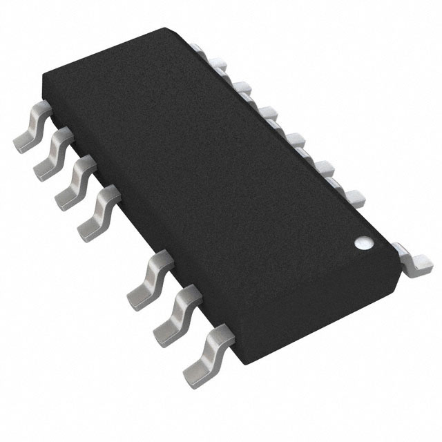


 工商网监
湘ICP备2023018690号
工商网监
湘ICP备2023018690号
