Product
Folder
Sample &
Buy
Technical
Documents
Support &
Community
Tools &
Software
UCC27210, UCC27211
SLUSAT7F – NOVEMBER 2011 – REVISED DECEMBER 2014
UCC2721x 120-V Boot, 4-A Peak, High-Frequency High-Side and Low-Side Driver
1 Features
3 Description
•
The UCC27210 and UCC27211 drivers are based on
the popular UCC27200 and UCC27201 MOSFET
drivers, but offer several significant performance
improvements. Peak output pull-up and pull-down
current has been increased to 4-A source and 4-A
sink, and pull-up and pull-down resistance have been
reduced to 0.9 Ω, thereby allowing for driving large
power MOSFETs with minimized switching losses
during the transition through the Miller Plateau of the
MOSFET. The input structure is now able to directly
handle –10 VDC, which increases robustness and
also allows direct interface to gate-drive transformers
without using rectification diodes. The inputs are also
independent of supply voltage and have a maximum
rating of 20-V.
1
•
•
•
•
•
•
•
•
•
•
•
•
Drives Two N-Channel MOSFETs in High-Side
and Low-Side Configuration With Independent
Inputs
Maximum Boot Voltage 120-V DC
4-A Sink, 4-A Source Output Currents
0.9-Ω Pullup and Pulldown Resistance
Input Pins Can Tolerate –10 V to 20 V and Are
Independent of Supply Voltage Range
TTL or Pseudo-CMOS Compatible Input Versions
8-V to 17-V VDD Operating Range, (20-V
Absolute Maximum)
7.2-ns Rise and 5.5-ns Fall Time With 1000-pF
Load
Fast Propagation Delay Times (18 ns Typical)
2-ns Delay Matching
Symmetrical Undervoltage Lockout for High-Side
and Low-Side Driver
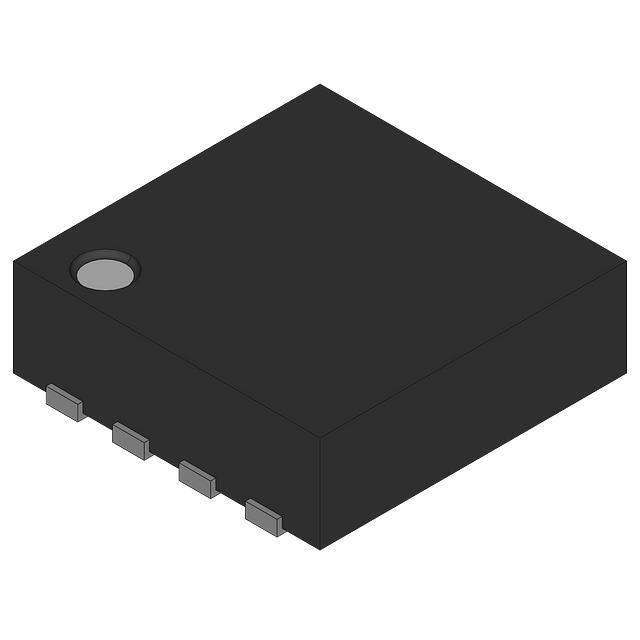
All Industry Standard Packages Available (SOIC8, PowerPAD™ SOIC-8, 4-mm × 4-mm SON-8
and 4-mm × 4-mm SON-10)
Specified from –40 to 140 °C
Device Information(1)
PART NUMBER
UCC27210,
UCC27211
PACKAGE
BODY SIZE (NOM)
SOIC (8)
4.90 mm × 3.91 mm
PowerPAD (8)
4.89 mm × 3.90 mm
WSON (10)
4.00 mm × 4.00 mm
VSON (8)
(1) For all available packages, see the orderable addendum at
the end of the datasheet.
2 Applications
•
•
•
•
•
•
•
Power Supplies for Telecom, Datacom, and
Merchant
Half-Bridge and Full-Bridge Converters
Push-Pull Converters
High-Voltage Synchronous-Buck Converters
Two-Switch Forward Converters
Active-Clamp Forward Converters
Class-D Audio Amplifiers
space
Typical Application: UCC27210
+12V
Typical Application: UCC27211
+12V
+100V
+100V
VDD
SECONDARY
SIDE
CIRCUIT
VDD
HB
HB
DRIVE
HI
LI
CONTROL
PWM
CONTROLLER
PWM
CONTROLLER
HO
LI
CONTROL
HI
DRIVE
HI
HI
SECONDARY
SIDE
CIRCUIT
HO
HS
DRIVE
LO
HS
LO
UCC27211
DRIVE
LO
LO
VSS
+12V
UCC27210
VDD
+100V
VSS
HB
HI
LI
CONTROL
ISOLATION
AND
FEEDBACK
DRIVE
HI
HO
HS
DRIVE
LO
LO
UCC27211
1
An IMPORTANT NOTICE at the end of this data sheet addresses availability, warranty, changes, use in safety-critical applications,
intellectual property matters and other important disclaimers. PRODUCTION DATA.
�UCC27210, UCC27211
SLUSAT7F – NOVEMBER 2011 – REVISED DECEMBER 2014
www.ti.com
Table of Contents
1
2
3
4
5
6
7
Features ..................................................................
Applications ...........................................................
Description .............................................................
Revision History.....................................................
Description (Continued) ........................................
Pin Configuration and Functions .........................
Specifications.........................................................
1
1
1
2
4
4
5
7.1
7.2
7.3
7.4
7.5
7.6
7.7
7.8
Absolute Maximum Ratings ...................................... 5
ESD Ratings ............................................................ 6
Recommended Operating Conditions....................... 6
Thermal Information .................................................. 6
Electrical Characteristics........................................... 7
Switching Characteristics: Propagation Delays ........ 8
Switching Characteristics: Delay Matching ............... 8
Switching Characteristics: Output Rise and Fall
Time ........................................................................... 8
7.9 Switching Characteristics: Miscellaneous ................. 8
7.10 Typical Characteristics .......................................... 10
8
Detailed Description ............................................ 13
8.1
8.2
8.3
8.4
9
Overview .................................................................
Functional Block Diagram .......................................
Feature Description.................................................
Device Functional Modes........................................
13
14
14
15
Application and Implementation ........................ 16
9.1 Application Information............................................ 16
9.2 Typical Application ................................................. 16
10 Power Supply Recommendations ..................... 21
11 Layout................................................................... 21
11.1 Layout Guidelines ................................................. 21
11.2 Layout Example .................................................... 22
11.3 Thermal Considerations ........................................ 22
12 Device and Documentation Support ................. 23
12.1
12.2
12.3
12.4
12.5
Documentation Support ........................................
Related Links ........................................................
Trademarks ...........................................................
Electrostatic Discharge Caution ............................
Glossary ................................................................
23
23
23
23
23
13 Mechanical, Packaging, and Orderable
Information ........................................................... 23
4 Revision History
NOTE: Page numbers for previous revisions may differ from page numbers in the current version.
Changes from Revision E (August 2013) to Revision F
•
Page
Added Pin Configuration and Functions section, ESD Ratings table, Feature Description section, Device Functional
Modes, Application and Implementation section, Power Supply Recommendations section, Layout section, Device
and Documentation Support section, and Mechanical, Packaging, and Orderable Information section .............................. 1
Changes from Revision D (November, 2012) to Revision E
Page
•
Added Note 2 to the Terminal Functions Table...................................................................................................................... 5
•
Changed Repetitive pulse data from -18 V to -(24V-VDD). ................................................................................................... 5
•
Added additional details to Note 2.......................................................................................................................................... 5
•
Changed Voltage on HS, VHS (repetitive pulse
很抱歉,暂时无法提供与“UCC27210DRMT”相匹配的价格&库存,您可以联系我们找货
免费人工找货- 国内价格 香港价格
- 1+29.545681+3.57806
- 10+22.2272810+2.69178
- 25+20.3922325+2.46955
- 100+18.37752100+2.22557
- 国内价格 香港价格
- 250+17.41635250+2.10917
- 500+16.83730500+2.03904
- 750+16.54719750+2.00391
- 1250+16.225781250+1.96499
- 1750+16.037971750+1.94224
- 2500+15.857332500+1.92036


 工商网监
湘ICP备2023018690号
工商网监
湘ICP备2023018690号
