UCC27512-EP
www.ti.com
SLUSBE3 – JUNE 2013
SINGLE CHANNEL HIGH-SPEED, LOW-SIDE GATE DRIVER
(WITH 4-A PEAK SOURCE AND 8-A PEAK SINK)
Check for Samples: UCC27512-EP
FEATURES
1
•
•
•
•
•
•
•
•
•
•
•
•
•
Low-Cost, Gate-Driver Device Offering
Superior Replacement of NPN and PNP
Discrete Solutions
4-A Peak Source and 8-A Peak Sink
Asymmetrical Drive
Strong Sink Current Offers Enhanced
Immunity Against Miller Turn On
Fast Propagation Delays (13-ns typical)
Fast Rise and Fall Times (9-ns and 7-ns
typical)
4.5-V to 18-V Single Supply Range
Outputs Held Low During VDD UVLO (ensures
glitch free operation at power-up and powerdown)
TTL and CMOS Compatible Input Logic
Threshold, (independent of supply voltage)
Hysteretic Logic Thresholds for High Noise
Immunity
Dual Input Design (choice of an inverting (INpin) or non-inverting (IN+ pin) driver
configuration)
– Unused Input Pin can be Used for Enable
or Disable Function
Output Held Low when Input Pins are Floating
Input Pin Absolute Maximum Voltage Levels
Not Restricted by VDD Pin Bias Supply
Voltage
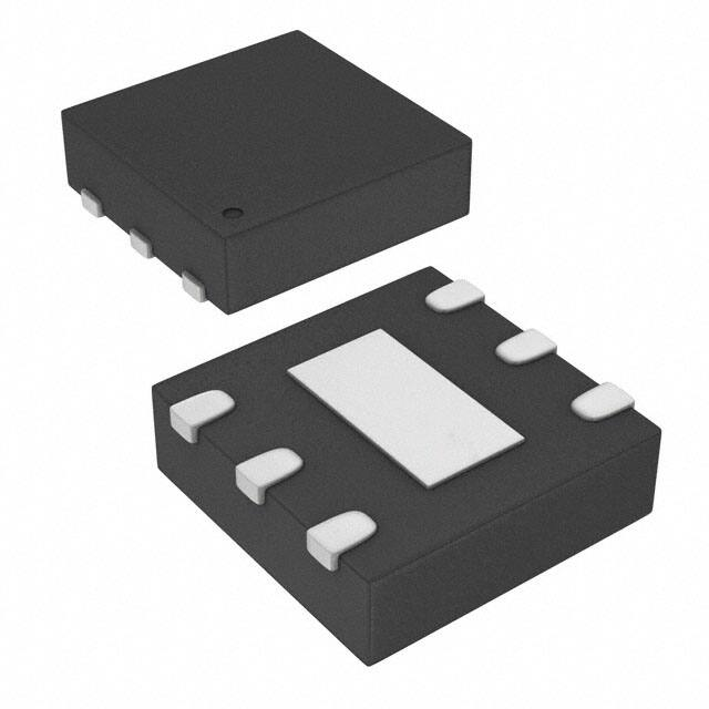
6-Pin DRS (3mm x 3 mm WSON with exposed
thermal pad) Package
APPLICATIONS
•
•
•
•
•
SUPPORTS DEFENSE, AEROSPACE,
AND MEDICAL APPLICATIONS
•
•
•
•
•
•
•
Controlled Baseline
One Assembly and Test Site
One Fabrication Site
Available in Military (–55°C to 125°C)
Temperature Range
Extended Product Life Cycle
Extended Product-Change Notification
Product Traceability
DESCRIPTION
The UCC27512 single-channel, high-speed, low-side
gate driver device is capable of effectively driving
MOSFET and IGBT power switches. Using a design
that inherently minimizes shoot-through current,
UCC27512 is capable of sourcing and sinking high,
peak-current pulses into capacitive loads offering railto-rail drive capability and extremely small
propagation delay typically 13 ns.
The UCC27512 provides 4-A source, 8-A sink
(asymmetrical drive) peak-drive current capability.
Strong sink capability in asymmetrical drive boosts
immunity against parasitic, Miller turn-on effect.
UCC27512 is designed to operate over a wide VDD
range of 4.5 V to 18 V and wide temperature range of
-55°C to 125°C. Internal Under Voltage Lockout
(UVLO) circuitry on VDD pin holds output low outside
VDD operating range. The capability to operate at low
voltage levels such as below 5 V, along with best in
class switching characteristics, is especially suited for
driving emerging wide band-gap power switching
devices such as GaN power semiconductor devices.
Switch-Mode Power Supplies
DC-to-DC Converters
Companion Gate Driver Devices for Digital
Power Controllers
Solar Power, Motor Control, UPS
Gate Driver for Emerging Wide Band-Gap
Power Devices (such as GaN)
1
Please be aware that an important notice concerning availability, standard warranty, and use in critical applications of
Texas Instruments semiconductor products and disclaimers thereto appears at the end of this data sheet.
PRODUCTION DATA information is current as of publication date.
Products conform to specifications per the terms of the Texas
Instruments standard warranty. Production processing does not
necessarily include testing of all parameters.
Copyright © 2013, Texas Instruments Incorporated
�UCC27512-EP
SLUSBE3 – JUNE 2013
www.ti.com
Typical Application Diagrams
Non-Inverting Input
Inverting Input
VSOURCE
VSOURCE
L1
L1
UCC27512
UCC27512
D1
IN+
1
IN+
IN-
D1
6
VOUT
1
IN+
2
3
IN-
6
GND
GND
5
VDD
OUT
4
IN-
Q1
2
GND
GND
5
R3
V+
3
VDD
OUT
4
C2
2
Q1
4.5 V to 18 V
+
4.5 V to 18 V
+
C1
R3
V+
C1
C2
Submit Documentation Feedback
Copyright © 2013, Texas Instruments Incorporated
Product Folder Links :UCC27512-EP
�UCC27512-EP
www.ti.com
SLUSBE3 – JUNE 2013
This integrated circuit can be damaged by ESD. Texas Instruments recommends that all integrated circuits be handled with
appropriate precautions. Failure to observe proper handling and installation procedures can cause damage.
ESD damage can range from subtle performance degradation to complete device failure. Precision integrated circuits may be more
susceptible to damage because very small parametric changes could cause the device not to meet its published specifications.
ORDERING INFORMATION (1) (2)
PART NUMBER
VID NUMBER
TOP-SIDE
MARKING
PACKAGE
PEAK CURRENT
(SOURCE/SINK)
INPUT THRESHOLD
LOGIC
OPERATING
TEMPERATURE
RANGE, TJ
UCC27512MDRSTEP
V62/13608-01XE
7512M
3 mm x 3 mm WSON,
6 pin
4-A/8-A
(Asymmetrical Drive)
CMOS/TTL-Compatible
(low voltage,
independent of VDD bias
voltage)
-55°C to 125°C
(1)
(2)
For the most current package and ordering information, see Package Option Addendum at the end of this document.
All packages use Pb-Free lead finish of Pd-Ni-Au which is compatible with MSL level 1 at 255°C to 260°C peak reflow temperature to be
compatible with either lead free or Sn/Pb soldering operations. DRS package is rated MSL level 2.
Table 1. UCC27512 Product Summary
PART NUMBER
PACKAGE
PEAK CURRENT (SOURCE/SINK)
INPUT THRESHOLD LOGIC
UCC27512MDRSTEP
3 mm x 3 mm WSON, 6 pin
4-A/8-A
(Asymmetrical Drive)
CMOS/TTL-Compatible
(low voltage, independent of VDD bias
voltage)
Submit Documentation Feedback
Copyright © 2013, Texas Instruments Incorporated
Product Folder Links :UCC27512-EP
3
�UCC27512-EP
SLUSBE3 – JUNE 2013
www.ti.com
ABSOLUTE MAXIMUM RATINGS (1) (2) (3)
over operating free-air temperature range (unless otherwise noted)
Supply voltage range
OUT voltage
MIN
MAX
VDD
-0.3
20
DC
-0.3 VDD + 0.3
Repetitive pulse less than 200 ns (4)
IOUT_DC (source)
0.3
IOUT_DC (sink)
0.6
Output pulsed current (0.5 µs)
(OUTH source current and OUTL sink current)
IOUT_pulsed(source)
4
IOUT_pulsed(sink)
8
IN+, INESD
-0.3
4000
Charged Device Model, CDM
1000
-55
150
Storage temperature range, TSTG
-65
150
(1)
(2)
(3)
(4)
(5)
4
A
20
Human Body Model, HBM
Junction temperature range, TJ
Lead temperature
V
-2 VDD + 0.3
Output continuous current
(OUTH source current and OUTL sink current)
(5)
UNIT
Soldering, 10 sec.
300
Reflow
260
V
°C
Stresses beyond those listed under “absolute maximum ratings” may cause permanent damage to the device. These are stress ratings
only and functional operation of the device at these or any other conditions beyond those indicated under “recommended operating
conditions” is not implied. Exposure to absolute-maximum-rated conditions for extended periods may affect device reliability.
All voltages are with respect to GND unless otherwise noted. Currents are positive into, negative out of the specified terminal. See
Packaging Section of the datasheet for thermal limitations and considerations of packages.
These devices are sensitive to electrostatic discharge; follow proper device handling procedures.
Values are verified by characterization on bench.
Maximum voltage on input pins is not restricted by the voltage on the VDD pin.
Submit Documentation Feedback
Copyright © 2013, Texas Instruments Incorporated
Product Folder Links :UCC27512-EP
�UCC27512-EP
www.ti.com
SLUSBE3 – JUNE 2013
RECOMMENDED OPERATING CONDITIONS
over operating free-air temperature range (unless otherwise noted)
MIN
TYP
Supply voltage range, VDD
4.5
12
18
V
Operating junction temperature range
-55
125
°C
0
18
V
Input voltage, IN+ and IN-
MAX
UNIT
THERMAL INFORMATION
UCC27512-EP
THERMAL METRIC (1)
DRS
UNITS
6 PINS
θJA
Junction-to-ambient thermal resistance (2)
85.6
θJCtop
Junction-to-case (top) thermal resistance (3)
100.1
θJB
Junction-to-board thermal resistance (4)
58.6
ψJT
Junction-to-top characterization parameter (5)
7.5
ψJB
Junction-to-board characterization parameter (6)
58.7
θJCbot
Junction-to-case (bottom) thermal resistance (7)
23.7
(1)
(2)
(3)
(4)
(5)
(6)
(7)
°C/W
For more information about traditional and new thermal metrics, see the IC Package Thermal Metrics application report, SPRA953.
The junction-to-ambient thermal resistance under natural convection is obtained in a simulation on a JEDEC-standard, high-K board, as
specified in JESD51-7, in an environment described in JESD51-2a.
The junction-to-case (top) thermal resistance is obtained by simulating a cold plate test on the package top. No specific JEDECstandard test exists, but a close description can be found in the ANSI SEMI standard G30-88.
The junction-to-board thermal resistance is obtained by simulating in an environment with a ring cold plate fixture to control the PCB
temperature, as described in JESD51-8.
The junction-to-top characterization parameter, ψJT, estimates the junction temperature of a device in a real system and is extracted
from the simulation data for obtaining θJA, using a procedure described in JESD51-2a (sections 6 and 7).
The junction-to-board characterization parameter, ψJB, estimates the junction temperature of a device in a real system and is extracted
from the simulation data for obtaining θJA , using a procedure described in JESD51-2a (sections 6 and 7).
The junction-to-case (bottom) thermal resistance is obtained by simulating a cold plate test on the exposed (power) pad. No specific
JEDEC standard test exists, but a close description can be found in the ANSI SEMI standard G30-88.
Spacer
Submit Documentation Feedback
Copyright © 2013, Texas Instruments Incorporated
Product Folder Links :UCC27512-EP
5
�UCC27512-EP
SLUSBE3 – JUNE 2013
www.ti.com
ELECTRICAL CHARACTERISTICS
VDD = 12 V, TJ = -55°C to 125°C, 1-µF capacitor from VDD to GND. Currents are positive into, negative out of the specified
terminal.
PARAMETER
TEST CONDITION
MIN
TYP
MAX
IN+ = VDD, IN- = GND
40
100
145
IN+ = IN- = GND or IN+ = IN- = VDD
25
75
138
IN+ = GND, IN- = VDD
20
60
110
UNITS
BIAS Currents
IDD(off)
Startup current
VDD = 3.4 V
µA
Under Voltage Lockout (UVLO)
VON
Supply start threshold
3.70
4.20
4.65
VOFF
Minimum operating
voltage after supply start
3.45
3.9
4.35
VDD_H
Supply voltage hysteresis
0.2
0.3
0.5
2.2
2.4
V
Inputs (IN+, IN-)
VIN_H
Input signal high
threshold
Output high for IN+ pin,
Output low for IN- pin
VIN_L
Input signal low threshold
Output low for IN+ pin,
Output high for IN- pin
1.0
VIN_HYS Input signal hysteresis
V
1.2
1.0
Source/Sink Current
ISRC/SNK
Source/sink peak
current (1)
CLOAD = 0.22 µF, FSW = 1 kHz
-4/+8
A
Outputs (OUTH, OUTL, OUT)
VDDVOH
VOL
ROH
ROL
(1)
(2)
6
High output voltage
Low output voltage
Output pull-up
resistance (2)
Output pull-down
resistance
VDD = 12 V
IOUTH = -10 mA
50
80
VDD = 4.5 V
IOUTH = -10 mA
60
125
VDD = 12
IOUTL = 10 mA
5
6
VDD = 4.5 V
IOUTL = 10 mA
5.5
9
VDD = 12 V
IOUTH = -10 mA
5
7.5
VDD = 4.5 V
IOUTH = -10 mA
5
10
VDD = 12 V
IOUTL = 10 mA
0.375
0.650
VDD = 4.5 V
IOUTL = 10 mA
0.45
0.750
mV
Ω
Ensured by Design.
ROH represents on-resistance of P-Channel MOSFET in pull-up structure of the UCC27512's output stage.
Submit Documentation Feedback
Copyright © 2013, Texas Instruments Incorporated
Product Folder Links :UCC27512-EP
�UCC27512-EP
www.ti.com
SLUSBE3 – JUNE 2013
ELECTRICAL CHARACTERISTICS (continued)
VDD = 12 V, TJ = -55°C to 125°C, 1-µF capacitor from VDD to GND. Currents are positive into, negative out of the specified
terminal.
PARAMETER
TEST CONDITION
MIN
TYP
MAX
8
12
16
22
VDD = 12 V
CLOAD = 1.8 nF, connected to OUTH and OUTL pins tied
together
7
11
VDD=4.5V
CLOAD = 1.8 nF
7
11
UNITS
Switching Time
tR
VDD = 12 V
CLOAD = 1.8 nF, connected to OUTH and OUTL pins tied
together
Rise time (3)
VDD = 4.5 V
CLOAD = 1.8 nF
tF
tD1
tD2
(3)
Fall time (3)
IN+ to output propagation
delay (3)
IN- to output propagation
delay (3)
VDD = 12 V
5-V input pulse CLOAD = 1.8 nF, connected to OUTH and
OUTL pins tied together
4
13
23
VDD = 4.5 V
5-V input pulse CLOAD = 1.8 nF, connected to OUTH and
OUTL pins tied together
4
15
26
VDD = 12 V
CLOAD = 1.8 nF, connected to OUTH and OUTL pins tied
together
4
13
23
VDD = 4.5 V
CLOAD = 1.8 nF, connected to OUTH and OUTL pins tied
together
4
19
30
ns
See timing diagrams in Figure 1, Figure 2, Figure 3 and Figure 4.
High
INPUT
(IN+ pin)
Low
High
IN- pin
Low
90%
OUTPUT
10%
tD1 t r
tD1 tf
Figure 1. Non-Inverting Configuration
(PWM Input to IN+ pin (IN- pin tied to GND),
Output represents OUTH and OUTL pins tied together)
Submit Documentation Feedback
Copyright © 2013, Texas Instruments Incorporated
Product Folder Links :UCC27512-EP
7
�UCC27512-EP
SLUSBE3 – JUNE 2013
www.ti.com
High
INPUT
(IN- pin)
Low
High
IN+ pin
Low
90%
OUTPUT
10%
tD2 tf
tD2 tr
Figure 2. Inverting Configuration
(PWM input to IN- pin (IN+ pin tied to VDD),
Output represents OUTH and OUTL pins tied together)
High
INPUT
(IN- pin)
Low
High
ENABLE
(IN+ pin)
Low
90%
OUTPUT
10%
tD1 tr
tD1
tf
Figure 3. Enable and Disable Function Using IN+ Pin
(Enable and disable signal applied to IN+ pin, PWM input to IN- pin,
Output represents OUTH and OUTL pins tied together)
High
INPUT
(IN+ pin)
Low
High
ENABLE
(IN- pin)
Low
90%
OUTPUT
10%
tD2 t f
tD2 tr
Figure 4. Enable and Disable Function Using IN- Pin
(Enable and disable signal applied to IN- pin, PWM input to IN+ pin,
Output represents OUTH and OUTL pins tied together)
8
Submit Documentation Feedback
Copyright © 2013, Texas Instruments Incorporated
Product Folder Links :UCC27512-EP
�UCC27512-EP
www.ti.com
SLUSBE3 – JUNE 2013
DEVICE INFORMATION
Functional Block Diagram
IN+
VDD
1
VDD
3
VDD
4
OUT
5
GND
230 kW
200 kW
IN-
6
VDD
GND
2
UVLO
DRS Package
(Top View)
IN+
1
6
IN-
GND
2
5
GND
VDD
3
4
OUT
TERMINAL FUNCTIONS
TERMINAL
I/O
FUNCTION
PIN NUMBER
NAME
1
IN+
I
Non-inverting input: When the driver is used in inverting configuration connect IN+
to VDD in order to enable output, OUT held LOW if IN+ is unbiased or floating.
2, 5
GND
-
Ground: All signals referenced to this pin. It is recommended to connect pin 2 and
pin 5 on PCB as close to the device as possible.
3
VDD
I
Bias supply input.
4
OUT
O
Sourcing/sinking current output of driver.
6
IN-
I
Inverting input: When the driver is used in non-inverting configuration connect IN- to
GND in order to enable output, OUT held LOW if IN- is unbiased or floating.
Table 2. Device Logic Table
(1)
IN+ PIN
IN- PIN
OUTH PIN
OUTL PIN
OUT
L
L
High impedance
L
L
L
H
High impedance
L
L
H
L
H
High impedance
H
H
H
High impedance
L
L
x (1)
Any
High impedance
L
L
Any
(1)
High impedance
L
L
x
x = Floating Condition
Submit Documentation Feedback
Copyright © 2013, Texas Instruments Incorporated
Product Folder Links :UCC27512-EP
9
�UCC27512-EP
SLUSBE3 – JUNE 2013
www.ti.com
TYPICAL CHARACTERISTICS
START-UP CURRENT
vs
TEMPERATURE
0.12
4.0
IN+ = Low, IN± = Low
Operating Supply Current (mA)
IN+ = High, IN± = Low
0.11
Startup Current (mA)
OPERATING SUPPLY CURRENT
vs
TEMPERATURE (Output Switching)
0.10
0.09
0.08
0.07
0.06
3.5
3.0
2.5
VDD = 12 V
CLoad = 500 pF
fSW = 500 kHz
VDD = 3.4 V
0.05
2.0
±60
±40
±20
0
20
40
60
80
100
120
Temperature (ƒC)
±40
±20
0
20
40
60
80
100
120
Temperature (ƒC)
C001
Figure 6.
SUPPLY CURRENT
vs
TEMPERATURE (Output in DC On/Off condition)
UVLO THRESHOLD VOLTAGE
vs
TEMPERATURE
4.6
IN+ = Low, IN± = Low
140
C013
Figure 5.
0.5
UVLO Rising
IN+ = High, IN± = Low
UVLO Falling
4.4
0.4
UVLO Threshold (V)
Operating Supply Current (mA)
±60
140
0.3
0.2
4.2
4.0
3.8
VDD = 12 V
0.1
3.6
±60
±40
±20
0
20
40
60
80
100
120
Temperature (ƒC)
3.5
±40
0
20
40
60
80
100
120
Temperature (ƒC)
140
C003
Figure 7.
Figure 8.
INPUT THRESHOLD
vs
TEMPERATURE
OUTPUT PULL-UP RESISTANCE
vs
TEMPERATURE
8
Turn-On
VDD = 12 V
CLoad = 1.8 nF
VDD = 12 V
IOUT = 10 mA
Output Pull-Up Resistance (
3.0
2.5
2.0
1.5
1.0
7
6
5
4
±60
±40
±20
0
20
40
60
Temperature (ƒC)
80
100
120
140
±60
±40
C014
Figure 9.
10
±20
C002
Turn-Off
Input Threshold (V)
±60
140
±20
0
20
40
60
Temperature (ƒC)
80
100
120
140
C004
Figure 10.
Submit Documentation Feedback
Copyright © 2013, Texas Instruments Incorporated
Product Folder Links :UCC27512-EP
�UCC27512-EP
www.ti.com
SLUSBE3 – JUNE 2013
TYPICAL CHARACTERISTICS (continued)
OUTPUT PULL-DOWN RESISTANCE
vs
TEMPERATURE
RISE TIME
vs
TEMPERATURE
8
VDD = 12 V
CLOAD = 1.8 nF
VDD = 12 V
IOUT = 10 mA
7
0.5
Rise Time (ns)
Output Pull-Down Resistance (
0.7
0.3
6
5
0.1
4
±60
±40
±20
0
20
40
60
80
100
120
±60
140
Temperature (ƒC)
±40
20
40
60
80
100
120
Figure 12.
FALL TIME
vs
TEMPERATURE
INPUT TO OUTPUT PROPAGATION DELAY
vs
TEMPERATURE
20
Turn-On
VDD = 12 V
CLoad = 1.8 nF
Propagation Delay (ns)
Turn-Off
9
8
7
6
140
C015
Figure 11.
VDD = 12 V
CLOAD = 1.8 nF
Fall Time (ns)
0
Temperature (ƒC)
10
15
10
5
±60
±40
±20
0
20
40
60
80
100
120
±60
140
Temperature (ƒC)
±20
0
20
40
60
80
100
120
Temperature (ƒC)
Figure 13.
Figure 14.
OPERATING SUPPLY CURRENT
vs
FREQUENCY
PROPAGATION DELAYS
vs
SUPPLY VOLTAGE
140
C006
20
VDD=4.5V
VDD=12V
VDD=15V
16
18
Propagation Delay (ns)
18
14
12
10
8
6
4
0
100
200
300
400
Frequency (kHz)
500
600
16
14
12
10
8
CLoad = 1.8 nF
2
0
±40
C016
20
Supply Current (mA)
±20
C005
700
6
Turn−On
Turn−Off
0
G010
Figure 15.
4
8
12
Supply Voltage (V)
16
20
G007
Figure 16.
Submit Documentation Feedback
Copyright © 2013, Texas Instruments Incorporated
Product Folder Links :UCC27512-EP
11
�UCC27512-EP
SLUSBE3 – JUNE 2013
www.ti.com
TYPICAL CHARACTERISTICS (continued)
RISE TIME
vs
SUPPLY VOLTAGE
FALL TIME
vs
SUPPLY VOLTAGE
20
10
Fall Time (ns)
Rise Time (ns)
8
15
10
6
4
5
0
4
8
12
Supply Voltage (V)
16
20
2
0
G008
Figure 17.
4
8
12
Supply Voltage (V)
16
20
G009
Figure 18.
APPLICATION INFORMATION
Introduction
High-current gate driver devices are required in switching power applications for a variety of reasons. In order to
effect fast switching of power devices and reduce associated switching power losses, a powerful gate driver can
be employed between the PWM output of controllers and the gates of the power semiconductor devices. Further,
gate drivers are indispensable when sometimes it is just not feasible to have the PWM controller directly drive
the gates of the switching devices. With advent of digital power, this situation will be often encountered since the
PWM signal from the digital controller is often a 3.3-V logic signal which is not capable of effectively turning on a
power switch. A level shifting circuitry is needed to boost the 3.3-V signal to the gate-drive voltage (such as 12 V)
in order to fully turn on the power device and minimize conduction losses. Traditional buffer drive circuits based
on NPN/PNP bipolar transistors in totem-pole arrangement, being emitter follower configurations, prove
inadequate with digital power since they lack level-shifting capability. Gate drivers effectively combine both the
level-shifting and buffer-drive functions. Gate drivers also find other needs such as minimizing the effect of highfrequency switching noise by locating the high-current driver physically close to the power switch, driving gatedrive transformers and controlling floating power-device gates, reducing power dissipation and thermal stress in
controllers by moving gate charge power losses into itself. Finally, emerging wide band-gap power device
technologies such as GaN based switches, which are capable of supporting very high switching frequency
operation, are driving very special requirements in terms of gate drive capability. These requirements include
operation at low VDD voltages (5 V or lower), low propagation delays and availability in compact, low-inductance
packages with good thermal capability. In summary gate-driver devices are extremely important components in
switching power combining benefits of high-performance, low cost, component count and board space reduction
and simplified system design.
12
Submit Documentation Feedback
Copyright © 2013, Texas Instruments Incorporated
Product Folder Links :UCC27512-EP
�UCC27512-EP
www.ti.com
SLUSBE3 – JUNE 2013
UCC27512 Product Summary
The UCC27512 is a single-channel, low-side high-speed gate driver devices featuring high-source/sink current
capability, industry best-in-class switching characteristics and a host of other features (Table 3) all of which
combine to ensure efficient, robust and reliable operation in high-frequency switching power circuits.
Table 3. UCC27512 Features and Benefits
FEATURE
BENEFIT
High Source and Sink Current Capability
4 A and 8 A (Asymmetrical)
4 A and 4 A (Symmetrical)
High current capability offers flexibility in employing UCC2751x
family of devices to drive a variety of power switching devices at
varying speeds
Best-in-class 13-ns (typ) Propagation delay
Extremely low pulse transmission distortion
Expanded VDD Operating range of 4.5 V to 18 V
Flexibility in system design
Low VDD operation ensures compatibility with emerging wide bandgap power devices such as GaN
Expanded Operating Temperature range of -55°C to 125°C
(See Electrical Characteristics table)
VDD UVLO Protection
Outputs are held low in UVLO condition, which ensures predictable,
glitch-free operation at power-up and power-down
Outputs held low when input pins (INx) in floating condition
Safety feature, especially useful in passing abnormal condition tests
during safety certification
Ability of input pins to handle voltage levels not restricted by VDD pin System simplification, especially related to auxiliary bias supply
bias voltage
architecture
Split output structure (OUTH, OUTL)
Allows independent optimization of turn-on and turn-off speeds
Strong sink current (8 A) and low pull-down impedance (0.375 Ω)
High immunity to C x dV/dt Miller turn-on events
CMOS/TTL compatible input threshold logic with wide hysteresis
Enhanced noise immunity, while retaining compatibility with
microcontroller logic level input signals (3.3 V, 5 V) optimized for
digital power
Submit Documentation Feedback
Copyright © 2013, Texas Instruments Incorporated
Product Folder Links :UCC27512-EP
13
�UCC27512-EP
SLUSBE3 – JUNE 2013
www.ti.com
Typical Application Diagram
Typical application diagram of UCC27512 is shown below illustrating use in non-inverting and inverting driver
configurations.
VSOURCE
L1
UCC27512
D1
IN+
1
IN+
6
IN-
VOUT
Q1
2
GND
GND
5
3
VDD
OUT
4
+
4.5 V to 18 V
R3
V+
C1
C2
Figure 19. Using Non-Inverting Input (IN- is grounded to enable output)
VSOURCE
L1
UCC27512
D1
1
IN+
2
GND
IN-
6
GND
5
INQ1
4.5 V to 18 V
+
R3
V+
3
VDD
OUT
4
C1
C2
Figure 20. Using Inverting Input (IN+ is tied to VDD enable output)
14
Submit Documentation Feedback
Copyright © 2013, Texas Instruments Incorporated
Product Folder Links :UCC27512-EP
�UCC27512-EP
www.ti.com
SLUSBE3 – JUNE 2013
VDD and Undervoltage Lockout
The UCC27512 has an internal Under Voltage LockOut (UVLO) protection feature on the VDD pin supply circuit
blocks. Whenever the driver is in UVLO condition (i.e. when VDD voltage less than VON during power up and
when VDD voltage is less than VOFF during power down), this circuit holds all outputs LOW, regardless of the
status of the inputs. The UVLO is typically 4.2 V with 300-mV typical hysteresis. This hysteresis helps prevent
chatter when low VDD supply voltages have noise from the power supply and also when there are droops in the
VDD bias voltage when the system commences switching and there is a sudden increase in IDD. The capability to
operate at low voltage levels such as below 5 V, along with best-in-class switching characteristics, is especially
suited for driving emerging GaN wide bandgap power semiconductor devices.
For example, at power up, the UCC27512 driver output remains LOW until the VDD voltage reaches the UVLO
threshold. The magnitude of the OUT signal rises with VDD until steady-state VDD is reached. In the non-inverting
operation (PWM signal applied to IN+ pin) shown below, the output remains LOW until the UVLO threshold is
reached, and then the output is in-phase with the input. In the inverting operation (PWM signal applied to IN- pin)
shown below the output remains LOW until the UVLO threshold is reached, and then the output is out-phase with
the input. In both cases, the unused input pin must be properly biased to enable the output. It is worth noting that
in these devices the output turns to high state only if IN+ pin is high and IN- pin is low after the UVLO threshold
is reached.
Since the driver draws current from the VDD pin to bias all internal circuits, for the best high-speed circuit
performance, two VDD bypass capacitors are recommended to prevent noise problems. The use of surface
mount components is highly recommended. A 0.1-μF ceramic capacitor should be located as close as possible to
the VDD to GND pins of the gate driver. In addition, a larger capacitor (such as 1 μF) with relatively low ESR
should be connected in parallel and close proximity, in order to help deliver the high-current peaks required by
the load. The parallel combination of capacitors should present a low impedance characteristic for the expected
current levels and switching frequencies in the application.
VDD
VDD Threshold
VDD Threshold
IN+
IN -
IN+
IN-
OUT
OUT
Figure 21. Power-Up (non-inverting drive)
Figure 22. Power-Up (inverting drive)
Operating Supply Current
The UCC27512 features very low quiescent IDD currents. The typical operating supply current in Under Voltage
LockOut (UVLO) state and fully-on state (under static and switching conditions) are summarized in Figure 5,
Figure 6 and Figure 7. The IDD current when the device is fully on and outputs are in a static state (DC high or
DC low, refer Figure 7) represents lowest quiescent IDD current when all the internal logic circuits of the device
are fully operational. The total supply current is the sum of the quiescent IDD current, the average IOUT current
due to switching and finally any current related to pull-up resistors on the unused input pin. For example when
the inverting input pin is pulled low additional current is drawn from VDD supply through the pull-up resistors
(refer to DEVICE INFORMATION for the device Block Diagram). Knowing the operating frequency (fSW) and the
MOSFET gate (QG) charge at the drive voltage being used, the average IOUT current can be calculated as
product of QG and fSW.
A complete characterization of the IDD current as a function of switching frequency at different VDD bias
voltages under 1.8-nF switching load is provided in Figure 15. The strikingly linear variation and close correlation
with theoretical value of average IOUT indicates negligible shoot-through inside the gate-driver device attesting to
its high-speed characteristics.
Submit Documentation Feedback
Copyright © 2013, Texas Instruments Incorporated
Product Folder Links :UCC27512-EP
15
�UCC27512-EP
SLUSBE3 – JUNE 2013
www.ti.com
Input Stage
The input pins of the UCC27512 is based on a TTL/CMOS compatible input threshold logic that is independent of
the VDD supply voltage. With typ high threshold = 2.2 V and typ low threshold = 1.2 V, the logic level thresholds
can be conveniently driven with PWM control signals derived from 3.3-V and 5-V digital power controllers. Wider
hysteresis (typ 1 V) offers enhanced noise immunity compared to traditional TTL logic implementations, where
the hysteresis is typically less than 0.5 V. These devices also feature tight control of the input pin threshold
voltage levels which eases system design considerations and ensures stable operation across temperature. The
very low input capacitance on these pins reduces loading and increases switching speed.
The device features an important safety function wherein, whenever any of the input pins are in a floating
condition, the output of the respective channel is held in the low state. This is achieved using VDD pull-up
resistors on all the inverting inputs (IN- pin) or GND pull-down resistors on all the non-inverting input pins (IN+
pin), (refer to DEVICE INFORMATION for the device Block Diagram).
The device also features a dual input configuration with two input pins available to control the state of the output.
The user has the flexibility to drive the device using either a non-inverting input pin (IN+) or an inverting input pin
(IN-). The state of the output pin is dependent on the bias on both the IN+ and IN- pins. Refer to the input/output
logic truth table (Table 2) and the Typical Application Diagrams, (Figure 19 and Figure 20), for additional
clarification.
Once an input pin has been chosen for PWM drive, the other input pin (the unused input pin) must be properly
biased in order to enable the output. As mentioned earlier, the unused input pin cannot remain in a floating
condition because whenever any input pin is left in a floating condition the output is disabled for safety purposes.
Alternatively, the unused input pin can effectively be used to implement an enable/disable function, as explained
below.
• In order to drive the device in a non-inverting configuration, apply the PWM control input signal to IN+ pin. In
this case, the unused input pin, IN-, must be biased low (eg. tied to GND) in order to enable the output.
– Alternately, the IN- pin can be used to implement the enable/disable function using an external logic
signal. OUT is disabled when IN- is biased high and OUT is enabled when IN- is biased low.
• In order to drive the device in an inverting configuration, apply the PWM control input signal to IN- pin. In this
case, the unused input pin, IN+, must be biased high (eg. tied to VDD) in order to enable the output.
– Alternately, the IN+ pin can be used to implement the enable/disable function using an external logic
signal. OUT is disabled when IN+ is biased low and OUT is enabled when IN+ is biased high.
• Finally, it is worth noting that the output pin can be driven into a high state ONLY when IN+ pin is biased high
and IN- input is biased low.
The input stage of the driver should preferably be driven by a signal with a short rise or fall time. Caution must be
exercised whenever the driver is used with slowly varying input signals, especially in situations where the device
is located in a mechanical socket or PCB layout is not optimal:
• High dI/dt current from the driver output coupled with board layout parasitics can cause ground bounce. Since
the device features just one GND pin which may be referenced to the power ground, this may modify the
differential voltage between input pins and GND and trigger an unintended change of output state. Because
of fast 13-ns propagation delay, this can ultimately result in high-frequency oscillations, which increases
power dissipation and poses risk of damage.
• 1-V input threshold hysteresis boosts noise immunity compared to most other industry standard drivers.
• In the worst case, when a slow input signal is used and PCB layout is not optimal, it may be necessary to add
a small capacitor (1 nF) between input pin and ground very close to the driver device. This helps to convert
the differential mode noise with respect to the input logic circuitry into common mode noise and avoid
unintended change of output state.
If limiting the rise or fall times to the power device is the primary goal, then an external resistance is highly
recommended between the output of the driver and the power device instead of adding delays on the input
signal. This external resistor has the additional benefit of reducing part of the gate charge related power
dissipation in the gate driver device package and transferring it into the external resistor itself.
16
Submit Documentation Feedback
Copyright © 2013, Texas Instruments Incorporated
Product Folder Links :UCC27512-EP
�UCC27512-EP
www.ti.com
SLUSBE3 – JUNE 2013
Enable Function
As mentioned earlier, an enable/disable function can be easily implemented in UCC27512 using the unused
input pin. When IN+ is pulled down to GND or IN- is pulled down to VDD, the output is disabled. Thus IN+ pin
can be used like an enable pin that is based on active high logic, while IN- can be used like an enable pin that is
based on active low logic.
Output Stage
The output stage of the UCC27512 is illustrated in Figure 23. OUTH and OUTL are internally connected and
pinned out as OUT pin. The UCC27512 features a unique architecture on the output stage which delivers the
highest peak source current when it is most needed during the Miller plateau region of the power switch turn-on
transition (when the power switch drain/collector voltage experiences dV/dt). The device output stage features a
hybrid pull-up structure using a parallel arrangement of N-Channel and P-Channel MOSFET devices. By turning
on the N-Channel MOSFET during a narrow instant when the output changes state from low to high, the gatedriver device is able to deliver a brief boost in the peak-sourcing current enabling fast turn on.
VCC
ROH
RNMOS, Pull Up
Input Signal Anti ShootThrough
Circuitry
Gate
Voltage
Boost
OUTH
OUTL
Narrow Pulse at
each Turn On
ROL
Figure 23. UCC27512 Gate Driver Output Structure
The ROH parameter (see ELECTRICAL CHARACTERISTICS) is a DC measurement and it is representative of
the on-resistance of the P-Channel device only, since the N-Channel device is turned on only during output
change of state from low to high. Thus the effective resistance of the hybrid pull-up stage is much lower than
what is represented by ROH parameter. The pull-down structure is composed of a N-Channel MOSFET only. The
ROL parameter (see ELECTRICAL CHARACTERISTICS), which is also a DC measurement, is representative of
true impedance of the pull-down stage in the device. In UCC27512, the effective resistance of the hybrid pull-up
structure is approximately 2.7 x ROL.
The UCC27512 is capable of delivering 4-A source, 8-A sink (asymmetrical drive) at VDD = 12 V. Strong sink
capability in asymmetrical drive results in a very low pull-down impedance in the driver output stage which boosts
immunity against parasitic, Miller turn on (C x dV/dt turn on) effect, especially where low gate-charge MOSFETs
or emerging wide band-gap GaN power switches are used.
An example of a situation where Miller turn on is a concern is synchronous rectification (SR). In SR application,
the dV/dt occurs on MOSFET drain when the MOSFET is already held in off state by the gate driver. The current
discharging the CGD Miller capacitance during this dV/dt is shunted by the pull-down stage of the driver. If the
pull-down impedance is not low enough then a voltage spike can result in the VGS of the MOSFET, which can
result in spurious turn-on. This phenomenon is illustrated in Figure 24. UCC27512 offers a best-in-class, 0.375-Ω
(typ) pull-down impedance boosting immunity against Miller turn on.
Submit Documentation Feedback
Copyright © 2013, Texas Instruments Incorporated
Product Folder Links :UCC27512-EP
17
�UCC27512-EP
SLUSBE3 – JUNE 2013
www.ti.com
VDS
VIN
Miller Turn-On Spike in VGS
CGD
Gate Driver
RG
COSS
ISNK
OUTL
VTH
VGS of
MOSFET
ON OFF
CGS
VIN
ROL
VDS of
MOSFET
Figure 24. Very Low Pull-Down Impedance, 4-A/8-A Asymmetrical Drive
(output stage mitigates Miller turn on effect)
Figure 25 and Figure 26 illustrate typical switching characteristics of UCC27512.
Figure 25. Typical Turn-On Waveform
(VDD = 10 V, CL = 1 nF)
Figure 26. Typical Turn-Off Waveform
(VDD = 10 V, CL = 1 nF)
The driver output voltage swings between VDD and GND providing rail-to-rail operation, thanks to the MOS
output stage which delivers very low dropout. The presence of the MOSFET body diodes also offers low
impedance to switching overshoots and undershoots. This means that in many cases, external Schottky diode
clamps may be eliminated. The outputs of these drivers are designed to withstand 500-mA reverse current
without either damage to the device or logic malfunction.
18
Submit Documentation Feedback
Copyright © 2013, Texas Instruments Incorporated
Product Folder Links :UCC27512-EP
�UCC27512-EP
www.ti.com
SLUSBE3 – JUNE 2013
Power Dissipation
Power dissipation of the gate driver has two portions as shown in equation below:
PDISS = PDC + PSW
(1)
The DC portion of the power dissipation is PDC = IQ x VDD where IQ is the quiescent current for the driver. The
quiescent current is the current consumed by the device to bias all internal circuits such as input stage, reference
voltage, logic circuits, protections etc and also any current associated with switching of internal devices when the
driver output changes state (such as charging and discharging of parasitic capacitances, parasitic shoot-through
etc). The UCC27512 features very low quiescent currents (less than 1 mA, refer Figure 7) and contains internal
logic to eliminate any shoot-through in the output driver stage. Thus the effect of the PDC on the total power
dissipation within the gate driver can be safely assumed to be negligible.
The power dissipated in the gate-driver package during switching (PSW) depends on the following factors:
• Gate charge required of the power device (usually a function of the drive voltage VG, which is very close to
input bias supply voltage VDD due to low VOH drop-out).
• Switching frequency.
• Use of external gate resistors.
When a driver device is tested with a discrete, capacitive load it is a fairly simple matter to calculate the power
that is required from the bias supply. The energy that must be transferred from the bias supply to charge the
capacitor is given by:
1
EG = CLOAD VDD2
2
(2)
Where CLOAD is load capacitor and VDD is bias voltage feeding the driver.
There is an equal amount of energy dissipated when the capacitor is charged. This leads to a total power loss
given by the following:
PG = CLOAD VDD2 fSW
(3)
where ƒSW is the switching frequency.
The switching load presented by a power MOSFET/IGBT can be converted to an equivalent capacitance by
examining the gate charge required to switch the device. This gate charge includes the effects of the input
capacitance plus the added charge needed to swing the drain voltage of the power device as it switches between
the ON and OFF states. Most manufacturers provide specifications of typical and maximum gate charge, in nC,
to switch the device under specified conditions. Using the gate charge Qg, one can determine the power that
must be dissipated when charging a capacitor. This is done by using the equation, QG = CLOAD x VDD, to provide
the following equation for power:
PG = CLOAD VDD2 fSW = Qg VDD fSW
(4)
This power PG is dissipated in the resistive elements of the circuit when the MOSFET/IGBT is being turned on or
off. Half of the total power is dissipated when the load capacitor is charged during turnon, and the other half is
dissipated when the load capacitor is discharged during turnoff. When no external gate resistor is employed
between the driver and MOSFET/IGBT, this power is completely dissipated inside the driver package. With the
use of external gate-drive resistors, the power dissipation is shared between the internal resistance of driver and
external gate resistor in accordance to the ratio of the resistances (more power dissipated in the higher
resistance component). Based on this simplified analysis, the driver power dissipation during switching is
calculated as follows:
ROFF
RON
PSW = QG ´ VDD ´ fSW ´ (
+
)
(ROFF +RGATE ) (RON +RGATE )
(5)
where ROFF = ROL and RON (effective resistance of pull-up structure) = 2.7 x ROL.
Submit Documentation Feedback
Copyright © 2013, Texas Instruments Incorporated
Product Folder Links :UCC27512-EP
19
�UCC27512-EP
SLUSBE3 – JUNE 2013
www.ti.com
Low Propagation Delays
The UCC27512 driver features best-in-class input-to-output propagation delay of 13 ns (typ) at VDD = 12 V. This
promises the lowest level of pulse transmission distortion available from industry standard gate driver devices for
high-frequency switching applications. As seen in Figure 14, there is very little variation of the propagation delay
with temperature and supply voltage as well, offering typically less than 20-ns propagation delays across the
entire range of application conditions.
Thermal Information
The useful range of a driver is greatly affected by the drive power requirements of the load and the thermal
characteristics of the package. In order for a gate driver to be useful over a particular temperature range the
package must allow for the efficient removal of the heat produced while keeping the junction temperature within
rated limits. The thermal metrics for the driver package is summarized in the Thermal Information section of the
datasheet. For detailed information regarding the thermal information table, please refer to the Application Note
from Texas Instruments entitled IC Package Thermal Metrics (Texas Instruments Literature Number SPRA953A).
The thermal pad in DRS package provides designers with an ability to create an excellent heat removal subsystem from the vicinity of the device, thus helping to maintain a lower junction temperature. This pad should be
soldered to the copper on the printed circuit board directly underneath the device package. Then a printed circuit
board designed with thermal lands and thermal vias completes a very efficient heat removal subsystem. In such
a design, the heat is extracted from the semiconductor junction through the thermal pad, which is then efficiently
conducted away from the location of the device on the PCB through the thermal network. This helps to maintain
a lower board temperature near the vicinity of the device leading to an overall lower device junction temperature.
Note that the exposed pad in DRS package is not directly connected to any leads of the package. However, it is
electrically and thermally connected to the substrate of the device which is the ground of the device. It is
recommended to externally connect the exposed pads to GND in PCB layout for better EMI immunity.
20
Submit Documentation Feedback
Copyright © 2013, Texas Instruments Incorporated
Product Folder Links :UCC27512-EP
�UCC27512-EP
www.ti.com
SLUSBE3 – JUNE 2013
PCB Layout
Proper PCB layout is extremely important in a high-current, fast-switching circuit to provide appropriate device
operation and design robustness. The UCC27512 gate driver incorporates short-propagation delays and powerful
output stages capable of delivering large current peaks with very fast rise and fall times at the gate of power
switch to facilitate voltage transitions very quickly. At higher VDD voltages, the peak-current capability is even
higher (4-A/8-A peak current is at VDD = 12 V). Very high di/dt can cause unacceptable ringing if the trace
lengths and impedances are not well controlled. The following circuit layout guidelines are strongly recommended
when designing with these high-speed drivers.
• Locate the driver device as close as possible to power device in order to minimize the length of high-current
traces between the output pins and the gate of the power device.
• Locate the VDD bypass capacitors between VDD and GND as close as possible to the driver with minimal
trace length to improve the noise filtering. These capacitors support high-peak current being drawn from VDD
during turnon of power MOSFET. The use of low inductance SMD components such as chip resistors and
chip capacitors is highly recommended.
• The turn-on and turn-off current loop paths (driver device, power MOSFET and VDD bypass capacitor) should
be minimized as much as possible in order to keep the stray inductance to a minimum. High dI/dt is
established in these loops at two instances – during turn-on and turn-off transients, which will induce
significant voltage transients on the output pin of the driver device and gate of the power switch.
• Wherever possible parallel the source and return traces, taking advantage of flux cancellation.
• Separate power traces and signal traces, such as output and input signals.
• Star-point grounding is a good way to minimize noise coupling from one current loop to another. The GND of
the driver should be connected to the other circuit nodes such as source of power switch, ground of PWM
controller etc at one, single point. The connected paths should be as short as possible to reduce inductance
and be as wide as possible to reduce resistance.
• Use a ground plane to provide noise shielding. Fast rise and fall times at OUT may corrupt the input signals
during transition. The ground plane must not be a conduction path for any current loop. Instead the ground
plane must be connected to the star-point with one single trace to establish the ground potential. In addition
to noise shielding, the ground plane can help in power dissipation as well.
• In noisy environments, it may be necessary to tie the unused Input pin of UCC27512 to VDD (in case of IN+)
or GND (in case of IN-) using short traces in order to ensure that the output is enabled and to prevent noise
from causing malfunction in the output.
• The UCC27512 offers two ground pins, pin 2 and pin 5. It is extremely important to short the two pins
together using the PCB trace. The shortest trace should be located as close as possible to the device.
Submit Documentation Feedback
Copyright © 2013, Texas Instruments Incorporated
Product Folder Links :UCC27512-EP
21
�PACKAGE OPTION ADDENDUM
www.ti.com
10-Dec-2020
PACKAGING INFORMATION
Orderable Device
Status
(1)
Package Type Package Pins Package
Drawing
Qty
Eco Plan
(2)
Lead finish/
Ball material
MSL Peak Temp
Op Temp (°C)
Device Marking
(3)
(4/5)
(6)
UCC27512MDRSTEP
ACTIVE
SON
DRS
6
250
RoHS & Green
NIPDAU
Level-2-260C-1 YEAR
-55 to 125
7512M
V62/13608-01XE
ACTIVE
SON
DRS
6
250
RoHS & Green
NIPDAU
Level-2-260C-1 YEAR
-55 to 125
7512M
(1)
The marketing status values are defined as follows:
ACTIVE: Product device recommended for new designs.
LIFEBUY: TI has announced that the device will be discontinued, and a lifetime-buy period is in effect.
NRND: Not recommended for new designs. Device is in production to support existing customers, but TI does not recommend using this part in a new design.
PREVIEW: Device has been announced but is not in production. Samples may or may not be available.
OBSOLETE: TI has discontinued the production of the device.
(2)
RoHS: TI defines "RoHS" to mean semiconductor products that are compliant with the current EU RoHS requirements for all 10 RoHS substances, including the requirement that RoHS substance
do not exceed 0.1% by weight in homogeneous materials. Where designed to be soldered at high temperatures, "RoHS" products are suitable for use in specified lead-free processes. TI may
reference these types of products as "Pb-Free".
RoHS Exempt: TI defines "RoHS Exempt" to mean products that contain lead but are compliant with EU RoHS pursuant to a specific EU RoHS exemption.
Green: TI defines "Green" to mean the content of Chlorine (Cl) and Bromine (Br) based flame retardants meet JS709B low halogen requirements of


 工商网监
湘ICP备2023018690号
工商网监
湘ICP备2023018690号
