Product
Folder
Sample &
Buy
Technical
Documents
Support &
Community
Tools &
Software
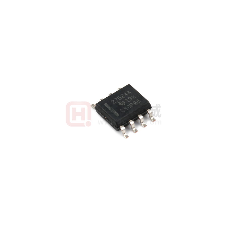
UCC27524A
SLUSBP4B – AUGUST 2013 – REVISED OCTOBER 2014
UCC27524A Dual 5-A, High-Speed, Low-Side Gate Driver With Negative Input Voltage
Capability
1 Features
3 Description
•
•
•
•
•
The UCC27524A device is a dual-channel, highspeed, low-side, gate-driver device capable of
effectively driving MOSFET and IGBT power
switches. The UCC27524A is a variant of the
UCC2752x family. The UCC27524A adds the ability
to handle –5 V directly at the input pins for increased
robustness. The UCC27524A is a dual non-inverting
driver. Using a design that inherently minimizes
shoot-through current, the UCC27524A is capable of
delivering high-peak current pulses of up to 5-A
source and 5-A sink into capacitive loads along with
rail-to-rail drive capability and extremely small
propagation delay typically 13 ns. In addition, the
drivers feature matched internal propagation delays
between the two channels which are very well suited
for applications requiring dual-gate drives with critical
timing, such as synchronous rectifiers. This also
enables connecting two channels in parallel to
effectively increase current-drive capability or driving
two switches in parallel with a single input signal. The
input pin thresholds are based on TTL and CMOS
compatible low-voltage logic, which is fixed and
independent of the VDD supply voltage. Wide
hysteresis between the high and low thresholds offers
excellent noise immunity.
1
•
•
•
•
•
•
•
•
•
•
•
•
Industry-Standard Pin Out
Two Independent Gate-Drive Channels
5-A Peak Source and Sink-Drive Current
Independent-Enable Function for Each Output
TTL and CMOS Compatible Logic Threshold
Independent of Supply Voltage
Hysteretic-Logic Thresholds for High Noise
Immunity
Ability to Handle Negative Voltages (–5 V) at
Inputs
Inputs and Enable Pin-Voltage Levels Not
Restricted by VDD Pin Bias Supply Voltage
4.5 to 18-V Single-Supply Range
Outputs Held Low During VDD-UVLO (Ensures
Glitch-Free Operation at Power Up and Power
Down)
Fast Propagation Delays (13-ns Typical)
Fast Rise and Fall Times (7-ns and 6-ns Typical)
1-ns Typical Delay Matching Between 2-Channels
Two Outputs are Paralleled for Higher Drive
Current
Outputs Held in Low When Inputs Floating
SOIC-8, HVSSOP-8 PowerPAD™ Package
Options
Operating Temperature Range of –40 to 140°C
2 Applications
•
•
•
•
Switch-Mode Power Supplies
DC-to-DC Converters
Motor Control, Solar Power
Gate Drive for Emerging Wide Band-Gap Power
Devices Such as GaN
Device Information(1)
PART NUMBER
UCC27524A
PACKAGE
BODY SIZE (NOM)
SOIC (8)
4.90 mm x 3.91 mm
HVSSOP (8)
3.00 mm x 3.00 mm
(1) For all available packages, see the orderable addendum at
the end of the datasheet.
Dual Non-Inverting Inputs
1
An IMPORTANT NOTICE at the end of this data sheet addresses availability, warranty, changes, use in safety-critical applications,
intellectual property matters and other important disclaimers. PRODUCTION DATA.
�UCC27524A
SLUSBP4B – AUGUST 2013 – REVISED OCTOBER 2014
www.ti.com
Table of Contents
1
2
3
4
5
6
7
8
Features ..................................................................
Applications ...........................................................
Description .............................................................
Revision History.....................................................
Description (Continued) ........................................
Pin Configuration and Functions .........................
Specifications.........................................................
1
1
1
2
3
3
4
7.1
7.2
7.3
7.4
7.5
7.6
7.7
4
4
4
5
6
6
8
Absolute Maximum Ratings ......................................
Handling Ratings.......................................................
Recommended Operating Conditions.......................
Thermal Information ..................................................
Electrical Characteristics...........................................
Switching Characteristics ..........................................
Typical Characteristics ..............................................
Detailed Description ............................................ 11
8.1 Overview ................................................................. 11
8.2 Functional Block Diagram ....................................... 12
8.3 Feature Description................................................. 12
8.4 Device Functional Modes........................................ 17
9
Applications and Implementation ...................... 18
9.1 Application Information............................................ 18
9.2 Typical Application .................................................. 18
10 Power Supply Recommendations ..................... 23
11 Layout................................................................... 23
11.1 Layout Guidelines ................................................. 23
11.2 Layout Example .................................................... 24
11.3 Thermal Protection................................................ 24
12 Device and Documentation Support ................. 26
12.1 Trademarks ........................................................... 26
12.2 Electrostatic Discharge Caution ............................ 26
12.3 Glossary ................................................................ 26
13 Mechanical, Packaging, and Orderable
Information ........................................................... 26
4 Revision History
Changes from Revision A (August 2013) to Revision B
•
Page
Added Pin Configuration and Functions section, Handling Rating table, Feature Description section, Device
Functional Modes, Application and Implementation section, Power Supply Recommendations section, Layout
section, Device and Documentation Support section, and Mechanical, Packaging, and Orderable Information
section ................................................................................................................................................................................... 1
Changes from Original (August 2013) to Revision A
Page
•
Changed marketing status from Product Preview to Production Data. .................................................................................. 1
•
Changed Enable voltage, ENA and ENB minimum from 0 to –2. .......................................................................................... 4
2
Submit Documentation Feedback
Copyright © 2013–2014, Texas Instruments Incorporated
Product Folder Links: UCC27524A
�UCC27524A
www.ti.com
SLUSBP4B – AUGUST 2013 – REVISED OCTOBER 2014
5 Description (Continued)
For safety purpose, internal pull-up and pull-down resistors on the input pins of the UCC27524A ensure that
outputs are held LOW when input pins are in floating condition. UCC27524A features Enable pins (ENA and
ENB) to have better control of the operation of the driver applications. The pins are internally pulled up to VDD
for active-high logic and are left open for standard operation.
UCC27524A family of devices are available in SOIC-8 (D), VSSOP-8 with exposed pad (DGN) packages.
6 Pin Configuration and Functions
8-Pin
D, DGN Package
Top View
ENA
1
8
ENB
INA
2
7
OUTA
GND
3
6
VDD
INB
4
5
OUTB
Pin Functions
PIN
I/O
DESCRIPTION
NAME
NO.
ENA
1
I
Enable input for Channel A: ENA is biased LOW to disable the Channel A output regardless of the
INA state. ENA is biased HIGH or left floating to enable the Channel A output. ENA is allowed to
float; hence the pin-to-pin compatibility with the UCC2732X N/C pin.
ENB
8
I
Enable input for Channel B: ENB is biased LOW to disables the Channel B output regardless of the
INB state. ENB is biased HIGH or left floating to enable Channel B output. ENB is allowed to float
hence; the pin-to-pin compatibility with the UCC2752A N/C pin.
GND
3
-
Ground: All signals are referenced to this pin.
INA
2
I
Input to Channel A: INA is the non-inverting input in the UCC27524A device. OUTA is held LOW if
INA is unbiased or floating.
INB
4
I
Input to Channel B: INB is the non-inverting input in the UCC27524A device. OUTB is held LOW if
INB is unbiased or floating.
OUTA
7
O
Output of Channel A
OUTB
5
O
Output of Channel B
VDD
6
I
Bias supply input
Submit Documentation Feedback
Copyright © 2013–2014, Texas Instruments Incorporated
Product Folder Links: UCC27524A
3
�UCC27524A
SLUSBP4B – AUGUST 2013 – REVISED OCTOBER 2014
www.ti.com
7 Specifications
7.1 Absolute Maximum Ratings (1) (2)
over operating free-air temperature range (unless otherwise noted)
Supply voltage range
OUTA, OUTB voltage
MIN
MAX
UNIT
VDD
–0.3
20
V
DC
–0.3
VDD + 0.3
V
–2
VDD + 0.3
V
0.3
A
5
A
Repetitive pulse < 200 ns (3)
Output continuous source/sink current
IOUT_DC
Output pulsed source/sink current (0.5 µs)
IOUT_pulsed
INA, INB, ENA, ENB voltage (4)
–5
20
V
Operating virtual junction temperature, TJ range
–40
150
°C
Soldering, 10 seconds
300
°C
Reflow
260
°C
Lead temperature
(1)
(2)
(3)
(4)
Stresses beyond those listed under Absolute Maximum Ratings may cause permanent damage to the device. These are stress ratings
only and functional operation of the device at these or any other conditions beyond those indicated under Recommended Operating
Conditions is not implied. Exposure to absolute-maximum-rated conditions for extended periods may affect device reliability.
All voltages are with respect to GND unless otherwise noted. Currents are positive into, negative out of the specified terminal. See
Packaging Section of the datasheet for thermal limitations and considerations of packages.
Values are verified by characterization on bench.
The maximum voltage on the Input and Enable pins is not restricted by the voltage on the VDD pin.
7.2 Handling Ratings
Tstg
V(ESD)
(1)
(2)
MIN
MAX
UNIT
–65
150
°C
Human body model (HBM), per ANSI/ESDA/JEDEC JS-001, all
pins (1)
–4000
4000
Charged device model (CDM), per JEDEC specification
JESD22-C101, all pins (2)
–1000
1000
Storage temperature range
Electrostatic discharge
V
JEDEC document JEP155 states that 500-V HBM allows safe manufacturing with a standard ESD control process.
JEDEC document JEP157 states that 250-V CDM allows safe manufacturing with a standard ESD control process.
7.3 Recommended Operating Conditions
over operating free-air temperature range (unless otherwise noted)
MIN
TYP
MAX
Supply voltage range, VDD
4.5
12
18
V
Operating junction temperature range
°C
–40
140
Input voltage, INA, INB
–2
18
Enable voltage, ENA and ENB
–2
18
4
Submit Documentation Feedback
UNIT
V
Copyright © 2013–2014, Texas Instruments Incorporated
Product Folder Links: UCC27524A
�UCC27524A
www.ti.com
SLUSBP4B – AUGUST 2013 – REVISED OCTOBER 2014
7.4 Thermal Information
THERMAL METRIC
UCC27524A
UCC27524A
SOIC (D)
MSOP (DGN) (1)
8 PINS
8 PINS
θJA
Junction-to-ambient thermal resistance (2)
130.9
71.8
θJCtop
Junction-to-case (top) thermal resistance (3)
80.0
65.6
(4)
θJB
Junction-to-board thermal resistance
71.4
7.4
ψJT
Junction-to-top characterization parameter (5)
21.9
7.4
ψJB
Junction-to-board characterization parameter (6)
70.9
31.5
θJCbot
Junction-to-case (bottom) thermal resistance (7)
n/a
19.6
(1)
(2)
(3)
(4)
(5)
(6)
(7)
UNIT
°C/W
For more information about traditional and new thermal metrics, see the IC Package Thermal Metrics application report, SPRA953.
The junction-to-ambient thermal resistance under natural convection is obtained in a simulation on a JEDEC-standard, high-K board, as
specified in JESD51-7, in an environment described in JESD51-2a.
The junction-to-case (top) thermal resistance is obtained by simulating a cold plate test on the package top. No specific JEDECstandard test exists, but a close description can be found in the ANSI SEMI standard G30-88.
The junction-to-board thermal resistance is obtained by simulating in an environment with a ring cold plate fixture to control the PCB
temperature, as described in JESD51-8.
The junction-to-top characterization parameter, ψJT, estimates the junction temperature of a device in a real system and is extracted
from the simulation data for obtaining θJA, using a procedure described in JESD51-2a (sections 6 and 7).
The junction-to-board characterization parameter, ψJB, estimates the junction temperature of a device in a real system and is extracted
from the simulation data for obtaining θJA , using a procedure described in JESD51-2a (sections 6 and 7).
The junction-to-case (bottom) thermal resistance is obtained by simulating a cold plate test on the exposed (power) pad. No specific
JEDEC standard test exists, but a close description can be found in the ANSI SEMI standard G30-88.
Spacer
Submit Documentation Feedback
Copyright © 2013–2014, Texas Instruments Incorporated
Product Folder Links: UCC27524A
5
�UCC27524A
SLUSBP4B – AUGUST 2013 – REVISED OCTOBER 2014
www.ti.com
7.5 Electrical Characteristics
VDD = 12 V, TA = TJ = –40 °C to 140 °C, 1-µF capacitor from VDD to GND. Currents are positive into, negative out of the
specified terminal (unless otherwise noted,)
PARAMETER
TEST CONDITION
MIN
TYP
MAX
VDD = 3.4 V,
INA = VDD,
INB = VDD
55
110
175
VDD = 3.4 V,
INA = GND,
INB = GND
25
75
145
3.91
4.2
4.5
UNIT
BIAS CURRENTS
Startup current,
(based on UCC27524 Input
configuration)
IDD(off)
μA
UNDER VOLTAGE LOCKOUT (UVLO)
TJ = 25 °C
VON
Supply start threshold
3.7
4.2
4.65
VOFF
Minimum operating voltage
after supply start
3.4
3.9
4.4
VDD_H
Supply voltage hysteresis
0.2
0.3
0.5
1.9
2.1
2.3
1
1.2
1.4
0.7
0.9
1.1
TJ = –40 °C to 140 °C
V
INPUTS (INA, INB, INA+, INA–, INB+, INB–), UCC27524A (D, DGN)
VIN_H
Input signal high threshold
Output high for non-inverting input pins
Output low for inverting input pins
VIN_L
Input signal low threshold
Output low for non-inverting input pins
Output high for inverting input pins
VIN_HYS
Input hysteresis
V
OUTPUTS (OUTA, OUTB)
ISNK/SRC
Sink/source peak current (1)
CLOAD = 0.22 µF, FSW = 1 kHz
VDD-VOH
High output voltage
IOUT = –10 mA
0.075
VOL
Low output voltage
IOUT = 10 mA
0.01
ROH
Output pullup resistance (2)
IOUT = –10 mA
2.5
5
7.5
Ω
ROL
Output pulldown resistance
IOUT = 10 mA
0.15
0.5
1
Ω
(1)
(2)
±5
A
V
Ensured by design.
ROH represents on-resistance of only the P-Channel MOSFET device in the pullup structure of the UCC27524A output stage.
7.6 Switching Characteristics
over operating free-air temperature range (unless otherwise noted)
TYP
MAX
tR
Rise time (1)
PARAMETER
CLOAD = 1.8 nF
7
18
tF
Fall time (1)
CLOAD = 1.8 nF
6
10
tM
Delay matching between 2 channels
INA = INB, OUTA and OUTB at 50%
transition point
1
4
tPW
Minimum input pulse width that
changes the output state
15
25
tD1, tD2
Input to output propagation delay (1)
CLOAD = 1.8 nF, 5-V input pulse
6
13
23
tD3, tD4
EN to output propagation delay (1)
CLOAD = 1.8 nF, 5-V enable pulse
6
13
23
(1)
6
TEST CONDITIONS
MIN
UNIT
ns
See the timing diagrams in Figure 1 and Figure 2
Submit Documentation Feedback
Copyright © 2013–2014, Texas Instruments Incorporated
Product Folder Links: UCC27524A
�UCC27524A
www.ti.com
SLUSBP4B – AUGUST 2013 – REVISED OCTOBER 2014
High
Input
Low
High
Enable
Low
90%
Output
10%
tD3
tD4
UDG-11217
Figure 1. Enable Function
(For Non-Inverting Input-Driver Operation)
High
Input
Low
High
Enable
Low
90%
Output
10%
tD1
tD2
UDG-11219
Figure 2. Non-Inverting Input-Driver Operation
Submit Documentation Feedback
Copyright © 2013–2014, Texas Instruments Incorporated
Product Folder Links: UCC27524A
7
�UCC27524A
SLUSBP4B – AUGUST 2013 – REVISED OCTOBER 2014
www.ti.com
7.7 Typical Characteristics
4
Operating Supply Current (mA)
Startup Current (mA)
0.14
Input=VDD
Input=GND
0.12
0.1
0.08
3.5
3
VDD = 12 V
fSW = 500 kHz
CL = 500 pF
VDD=3.4V
0.06
−50
0
50
Temperature (°C)
100
2.5
−50
150
0
G001
Figure 3. Start-Up Current vs Temperature
0.5
UVLO Threshold (V)
Supply Current (mA)
0.4
0.3
Enable=12 V
VDD = 12 V
0
50
Temperature (°C)
100
4.5
4
3.5
3
−50
150
0
G012
2.5
2.5
2
2
VDD = 12 V
1.5
1
50
Temperature (°C)
100
150
G003
VDD = 12 V
1
Enable High Threshold
Enable Low Threshold
150
0.5
−50
G004
Figure 7. Input Threshold vs Temperature
100
1.5
Input High Threshold
Input Low Threshold
0
50
Temperature (°C)
Figure 6. UVLO Threshold vs Temperature
Enable Threshold (V)
Input Threshold (V)
G002
UVLO Rising
UVLO Falling
Figure 5. Supply Current vs Temperature (Outputs In DC
On/Off Condition)
8
150
5
Input=GND
Input=VDD
0.5
−50
100
Figure 4. Operating Supply Current vs Temperature
(Outputs Switching)
0.6
0.2
−50
50
Temperature (°C)
0
50
Temperature (°C)
100
150
G005
Figure 8. Enable Threshold vs Temperature
Submit Documentation Feedback
Copyright © 2013–2014, Texas Instruments Incorporated
Product Folder Links: UCC27524A
�UCC27524A
www.ti.com
SLUSBP4B – AUGUST 2013 – REVISED OCTOBER 2014
Typical Characteristics (continued)
1
VDD = 12 V
IOUT = −10 mA
Output Pull−down Resistance (Ω)
Output Pull−up Resistance (Ω)
7
6
5
4
3
−50
0
50
Temperature (°C)
100
VDD = 12 V
IOUT = 10 mA
0.8
0.6
0.4
0.2
−50
150
Figure 9. Output Pullup Resistance vs Temperature
G007
8
Fall Time (ns)
Rise Time (ns)
150
VDD = 12 V
CLOAD = 1.8 nF
9
8
7
7
6
6
0
50
Temperature (°C)
100
5
−50
150
0
G008
Figure 11. Rise Time vs Temperature
50
Temperature (°C)
100
150
G009
Figure 12. Fall Time vs Temperature
18
18
Turn−on
Turn−off
EN to Output Propagation Delay (ns)
Input to Output Propagation Delay (ns)
100
9
VDD = 12 V
CLOAD = 1.8 nF
16
14
12
10
VDD = 12 V
CLOAD = 1.8 nF
8
−50
50
Temperature (°C)
Figure 10. Output Pulldown Resistance vs Temperature
10
5
−50
0
G006
0
50
Temperature (°C)
100
150
EN to Output High
EN to Output Low
16
14
12
10
VDD = 12 V
CLOAD = 1.8 nF
8
−50
G010
Figure 13. Input to Output Propagation Delay vs
Temperature
0
50
Temperature (°C)
100
150
G011
Figure 14. En to Output Propagation Delay vs Temperature
Submit Documentation Feedback
Copyright © 2013–2014, Texas Instruments Incorporated
Product Folder Links: UCC27524A
9
�UCC27524A
SLUSBP4B – AUGUST 2013 – REVISED OCTOBER 2014
www.ti.com
Typical Characteristics (continued)
22
VDD = 4.5 V
VDD = 12 V
VDD = 15 V
50
Propagation Delays (ns)
Operating Supply Current (mA)
60
40
CLOAD = 1.8 nF
Both channels switching
30
20
Input to Output On delay
Input to Ouptut Off Delay
EN to Output On Delay
EN to Output Off Delay
18
14
10
10
0
CLOAD = 1.8 nF
0
6
100 200 300 400 500 600 700 800 900 1000
Frequency (kHz)
G013
Figure 15. Operating Supply Current vs Frequency
4
8
12
Supply Voltage (V)
G014
10
CLOAD = 1.8 nF
CLOAD = 1.8 nF
14
Fall Time (ns)
Rise Time (ns)
20
Figure 16. Propagation Delays vs Supply Voltage
18
10
6
16
4
8
12
Supply Voltage (V)
16
8
6
4
20
4
8
12
Supply Voltage (V)
G015
Figure 17. Rise Time vs Supply Voltage
16
20
G016
Figure 18. Fall Time vs Supply Voltage
2.5
VDD = 4.5 V
Enable Threshold (V)
Enable High Threshold
Enable Low Threshold
2
1.5
1
0.5
−50
0
50
Temperature (°C)
100
150
G017
Figure 19. Enable Threshold vs Temperature
10
Submit Documentation Feedback
Copyright © 2013–2014, Texas Instruments Incorporated
Product Folder Links: UCC27524A
�UCC27524A
www.ti.com
SLUSBP4B – AUGUST 2013 – REVISED OCTOBER 2014
8 Detailed Description
8.1 Overview
The UCC27524A device represents Texas Instruments’ latest generation of dual-channel low-side high-speed
gate-driver devices featuring a 5-A source and sink current capability, industry best-in-class switching
characteristics, and a host of other features listed in Table 1 all of which combine to ensure efficient, robust and
reliable operation in high-frequency switching power circuits.
Table 1. UCC27524A Features and Benefits
FEATURE
BENEFIT
Best-in-class 13-ns (typ) propagation delay
Extremely low-pulse transmission distortion
1-ns (typ) delay matching between channels
Ease of paralleling outputs for higher (2 times) current capability,
ease of driving parallel-power switches
Expanded VDD Operating range of 4.5 to 18 V
Expanded operating temperature range of –40 °C to +140 °C
(See Electrical Characteristics table)
Flexibility in system design
VDD UVLO Protection
Outputs are held Low in UVLO condition, which ensures predictable,
glitch-free operation at power-up and power-down
Outputs held Low when input pins (INx) in floating condition
Safety feature, especially useful in passing abnormal condition tests
during safety certification
Outputs enable when enable pins (ENx) in floating condition
Pin-to-pin compatibility with the UCC27324 device from Texas
Instruments, in designs where Pin 1 and Pin 8 are in floating
condition
CMOS/TTL compatible input and enable threshold with wide
hysteresis
Enhanced noise immunity, while retaining compatibility with
microcontroller logic-level input signals (3.3 V, 5 V) optimized for
digital power
Ability of input and enable pins to handle voltage levels not restricted System simplification, especially related to auxiliary bias supply
by VDD pin bias voltage
architecture
Ability to handle –5 VDC (max) at input pins
Increased robustness in noisy environments
Submit Documentation Feedback
Copyright © 2013–2014, Texas Instruments Incorporated
Product Folder Links: UCC27524A
11
�UCC27524A
SLUSBP4B – AUGUST 2013 – REVISED OCTOBER 2014
www.ti.com
8.2 Functional Block Diagram
VDD
VDD
200 kW
ENA
200 kW
1
8
ENB
VDD
INA
OUTA
2
7
400 kW
VDD
VDD
VDD
UVLO
GND
6
3
VDD
INB
OUTB
4
5
400 kW
8.3 Feature Description
8.3.1 Operating Supply Current
The UCC27524A products feature very low quiescent IDD currents. The typical operating-supply current in UVLO
state and fully-on state (under static and switching conditions) are summarized in Figure 3, Figure 4 and
Figure 5. The IDD current when the device is fully on and outputs are in a static state (DC high or DC low, see
Figure 4) represents lowest quiescent IDD current when all the internal logic circuits of the device are fully
operational. The total supply current is the sum of the quiescent IDD current, the average IOUT current because of
switching, and finally any current related to pullup resistors on the enable pins and inverting input pins. For
example when the inverting input pins are pulled low additional current is drawn from the VDD supply through the
pullup resistors (see though ). Knowing the operating frequency (fSW) and the MOSFET gate (QG) charge at the
drive voltage being used, the average IOUT current can be calculated as product of QG and fSW.
A complete characterization of the IDD current as a function of switching frequency at different VDD bias voltages
under 1.8-nF switching load in both channels is provided in Figure 15. The strikingly linear variation and close
correlation with theoretical value of average IOUT indicates negligible shoot-through inside the gate-driver device
attesting to its high-speed characteristics.
8.3.2 Input Stage
The input pins of UCC27524A gate-driver devices are based on a TTL and CMOS compatible input-threshold
logic that is independent of the VDD supply voltage. With typically high threshold = 2.1 V and typically low
threshold = 1.2 V, the logic level thresholds are conveniently driven with PWM control signals derived from 3.3-V
and 5-V digital power-controller devices. Wider hysteresis (typ 0.9 V) offers enhanced noise immunity compared
to traditional TTL logic implementations, where the hysteresis is typically less than 0.5 V. UCC27524A devices
also feature tight control of the input pin threshold voltage levels which eases system design considerations and
ensures stable operation across temperature (refer to Figure 7). The very low input capacitance on these pins
reduces loading and increases switching speed.
12
Submit Documentation Feedback
Copyright © 2013–2014, Texas Instruments Incorporated
Product Folder Links: UCC27524A
�UCC27524A
www.ti.com
SLUSBP4B – AUGUST 2013 – REVISED OCTOBER 2014
Feature Description (continued)
The UCC27524A device features an important safety feature wherein, whenever any of the input pins is in a
floating condition, the output of the respective channel is held in the low state. This is achieved using GND
pulldown resistors on all the non-inverting input pins (INA, INB), as shown in the device block diagrams.
The input stage of each driver is driven by a signal with a short rise or fall time. This condition is satisfied in
typical power supply applications, where the input signals are provided by a PWM controller or logic gates with
fast transition times (


 工商网监
湘ICP备2023018690号
工商网监
湘ICP备2023018690号
