User’s Guide
UCC28514 User’s Guide
User’s Guide
�EVM IMPORTANT NOTICE (CATEGORY B)
IMPORTANT: TI is providing the enclosed HPA013B/HPA020A evaluation module under the
following conditions:
This evaluation module (EVM) being provided by Texas Instruments (TI) is intended for use for
ENGINEERING DEVELOPMENT OR EVALUATION PURPOSES ONLY and is not considered
by Texas Instruments to be fit for commercial use. As such, this EVM may not be complete in
terms of design and/or manufacturing related protective considerations including product safety
measures typically found in the end−product incorporating the module. As a prototype, this
product does not fall within the scope of the European Union Directive on electromagnetic
compatibility and on low voltage and therefore may not meet the technical requirements of the
directive. This EVM is not subject to the EU marking requirements.
2
•
Should this EVM not meet the specifications indicated in the User’s Guide the EVM may be
returned within 30 days from the date of delivery for a full refund. THE FOREGOING
WARRANTY IS THE EXCLUSIVE WARRANTY MADE BY TI AND IS IN LIEU OF ALL
OTHER WARRANTIES, EXPRESSED, IMPLIED, OR STATUTORY, INCLUDING ANY
WARRANTY OF MERCHANTABILITY OR FITNESS FOR ANY PARTICULAR PURPOSE.
•
The user assumes all responsibility and liability for proper and safe handling of the EVM.
The user acknowledge that the use of the EVM could present serious hazards and that it is
the user’s responsibility to take all precautions for the handling and use of the EVMs in
accordance with good laboratory practices. Please be aware that the products received may
not be regulatory compliant or agency certified (FCC, UL, etc.). Due to the open construction
of the product, it is the user’s responsibility to take any and all appropriate precautions with
regard to electrostatic discharge.
•
NEITHER PARTY WILL BE LIABLE TO THE OTHER FOR ANY INDIRECT, SPECIAL,
INCIDENTAL, OR CONSEQUENTIAL DAMAGES.
•
TI is currently dealing with various customers for products, and therefore our arrangement
with the user will not be exclusive.
•
TI assumes no liability for applications assistance, customer product design, software
performance, or infringement of patents or services described herein.
•
Please read the User’s Guide and specifically the section in the User’s Guide pertaining to
warnings and restrictions prior to handling the product. This section contains important
information regarding high temperature and voltages which TI recommends to be read
before handling the EVMs. In case of any doubt regarding safety, please contact the TI
application engineer.
•
Persons handling the product should have electronics training and observe good laboratory
practice standards.
•
No license is granted under any patent right or other intellectual property right of TI covering
or relating to any combination, machine, or process in which such TI products or services
might be or are used.
•
This Agreement is subject to the laws of the State of Texas, excluding the body of conflicts of
laws and the United Nations Convention on the International Sale of Goods, and will be
subject to the exclusive jurisdiction of the courts of the State of Texas.
�DYNAMIC WARNINGS AND RESTRICTIONS
It is important to operate this EVM within the maximum input voltage ranges specified in section 6.
Exceeding the specified input range may cause unexpected operation and/or irreversible damage to the EVM.
If there are questions concerning the input range, please contact a TI field representative prior to connecting
the input power.
Applying loads outside of the specified output range may result in unintended operation and/or possible
permanent damage to the EVM. Please consult the EVM User’s Guide prior to connecting any load to the EVM
output. If there is uncertainty as to the load specification, please contact a TI field representative.
During normal operation, some circuit components may have case temperatures greater than 50°C. The EVM
is designed to operate properly with certain components above 50°C as long as the input and output ranges are
maintained. These components include but are not limited to linear regulators, switching transistors, pass
transistors, and current sense resistors. These types of devices can be identified using the EVM schematic
located in the EVM User’s Guide. When placing measurement probes near these devices during operation,
please be aware that these devices may be very warm to the touch.
Mailing Address:
Texas Instruments
Post Office Box 655303
Dallas, Texas 75265
Copyright 2003, Texas Instruments Incorporated
3
�SLUU165A − November 2003 − Revised July 2004
UCC28514 User’s Guide
Power Supply Control Products
Contents
1
Introduction . . . . . . . . . . . . . . . . . . . . . . . . . . . . . . . . . . . . . . . . . . . . . . . . . . . . . . . . . . . . . . . . . . . . . . . . . 4
2
Caution . . . . . . . . . . . . . . . . . . . . . . . . . . . . . . . . . . . . . . . . . . . . . . . . . . . . . . . . . . . . . . . . . . . . . . . . . . . . . 4
3
Schematic . . . . . . . . . . . . . . . . . . . . . . . . . . . . . . . . . . . . . . . . . . . . . . . . . . . . . . . . . . . . . . . . . . . . . . . . . . . 5
4
List of Materials . . . . . . . . . . . . . . . . . . . . . . . . . . . . . . . . . . . . . . . . . . . . . . . . . . . . . . . . . . . . . . . . . . . . . 8
5
Reference Design Layout . . . . . . . . . . . . . . . . . . . . . . . . . . . . . . . . . . . . . . . . . . . . . . . . . . . . . . . . . . . . 11
6
Electrical Characteristics . . . . . . . . . . . . . . . . . . . . . . . . . . . . . . . . . . . . . . . . . . . . . . . . . . . . . . . . . . . . 12
7
Reference Design Performance . . . . . . . . . . . . . . . . . . . . . . . . . . . . . . . . . . . . . . . . . . . . . . . . . . . . . . 13
1
Introduction
The UCC28514 module is a 100-W offline ac-to-dc voltage converter with power factor
correction (PFC). The prototype was designed to show how the UCC28514 could be configured
to control a dc-regulated output offline with one control integrated circuit. The module was
design to operate over a universal input range of 85 V to 265 V with a regulated 24-V, 100-W
output.
To correctly operate this EVM a fan is required to keep the ambient temperature at or below
40°C. Not keeping the temperature at or below 40°C could damage the EVM.
2
Caution
High-voltage levels are present on the evaluation module whenever it is energized. Proper
precautions must be taken when working with the module. The evaluation module has a large
energy storage capacitor and must be completely discharged before the module can be
handled. Serious injury can occur if proper safety precautions are not followed.
4
UCC28514 User’s Guide
�SLUU165A − November 2003 − Revised July 2004
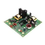
Schematic
The schematic is broken up into three sections to make it more legible for the user.
+
3
Figure 1. Mother Board HPA013
UCC28514 User’s Guide
5
�+
SLUU165A − November 2003 − Revised July 2004
Figure 2. Mother Board HPA013
6
UCC28514 User’s Guide
�+
SLUU165A − November 2003 − Revised July 2004
Figure 3. Daughter Board HPA020
UCC28514 User’s Guide
7
�SLUU165A − November 2003 − Revised July 2004
4
List of Materials
Table 1 lists the components used in this design. With minor component tweaks this design
could be modified to meet a wide range of applications.
Table 1. Mother Board List of Materials
REFERENCE
QTY
DESCRIPTION
MANUFACTURER
PART NUMBER
AC_L1
0
Connector, binding post, insulated, for standard banana
plug, black, 15 A, 141860
Johnson
111−0703−001
AC_N1
0
Connector, binding post, insulated, for standard banana
plug, red, 15 A, 141860
Johnson
111−0702−001
C1
1
Capacitor, film, 0.047 µF, 300 VAC, ±20%, 0.236 x 0.591
Panasonic
ECQU3A473MG
C2
1
Capacitor, polyester, .047 µF, 630 V, 10%, 0.256 x 0.650
Panasonic
ECQ−E6473KZ
C3
1
Capacitor, electrolytic, 100 µF, 450 V, TS series
Panasonic
ECO−S2WB101BA
C4, C9
2
Capacitor, ceramic, 1 µF, 25 V, X7R, 10%, 1206
Panasonic
ECJ−3YB1E105K
C5, C6, C15
3
Capacitor, film, 1.0 µF, 50 V, 5%, 7380
Panasonic
ECQ−V1H105JL
C7, C8
2
Capacitor, ceramic, 0.1 µF, 50 V, X7R, +\−10%, 43200
Panasonic
ECU−S1H104KBB
C10
1
Capacitor, film, 0.01 µF, 300 VAC, ±20%, 0.197 x 0.591
Panasonic
ECQU3A103MG
C11
1
Capacitor, ceramic, 0.01 µF, 50 V, X7R, 10%, 1206
Panasonic − ECG
ECU−V1H103KBM
C12
1
Capacitor, ceramic, 1 nF, 50 V, X7R, 10%, 805
Panasonic
ECU−V1H102KBN
C13
1
Capacitor, ceramic, 1 µF, 50 V, X7R, 10%, 1206
Panasonic
ECJ−3YB1E105K
C14
1
Capacitor, electrolytic, 270 µF, 35 V, 0.394 x 0.630
Panasonic
EEUFC1V271
C16
1
Capacitor, ceramic, 0.0015 µF, 50 V, X7R, 10%, 805
Panasonic
ECJ−2VB2D152K
Daughter Card
1
Controller board plugs into J1
Any
HPA020
D1
1
Bridge rectifier, 6 A, 600 V, GBJ series
General Semiconductor
PB66
D2
1
Diode, 600 V, 6 A, 400 A peak surge, 252000
Diodes Inc
6A6−T
D3
1
Diode, ultra fast, 8 A, 600 V, 5 mA
International Rectifier
HFA08TB60
D4, D12
2
Adjustable precision shunt regulator, SOT−89
Texas Instruments
TL431CPK
D5
1
Diode, rectifier, 2 A, 50 V, SMA
Vishay
BYG22A
D7, D6
2
Diode, schottky, 1.5 A, 25 V, SMA
Vishay
BYS10−25
D8
1
Diode, zener, 18 V, 83 mA, 1 W, DO−41
On Semi
1N4746
D10, D9
2
Diode, fast recovery, SOD−57
Phillips
BYV26
D11
1
Diode, dual schottky, 1.5 A, 100 V, TO220
OnSemi
MBR20100CT
D13
1
Diode, zener, 10 V, 35 mA, 350 mW, SOT23
Diodes Inc
BZX84C10−7
F1
1
Fuseholder, 1/4 fuses, 0.42
Cooper/Bussman
BK/1A1907−06
Fuse at F1
1
6 A, 250 V, 3AG Glass Fast Acting *Cartridge Type,
1.25” x 0.25”
Littlefuse
312 006
HS1
1
Heatsink, TO−220, vertical mount, 5*C/W, 0.5 x 1.38in.
Aavid
513201
HS2
1
Heatsink, TO−220, Vertical mount, 0.98 x 0.44
Aavid
579402B00000
HS3, HS4, HS5
3
Heatsink, TO−220, Vertical mount, 15°C/W, 0.5” x 0.95”
Aavid
593002B33402
J1**
1
Receptacle, female 28 pins, 0.197 x 1181
Hirose Electric
DF11−28DS−2DSA(xx)
L1**
1
Inductor, 50 µH, 5.6 A, 21.5 mΩ, 1,102 X 1,102
Cooper
CTX16−16366
OUT+1
0
Connector, binding post, insulated, for standard banana
plug, black, 15 A, 141860
Johnson
111−0703−001
PCB
1
Mother board
Any
HPA013
Q1, Q3, Q4**
3
MOSFET, N-channel, 500 V, 5 A, 1500 mΩ, TO−220
International Rectifier
IRF830A
Q2**
1
Bipolar, NPN, 400 V, 1 A, 15 W, DPAK
On Semi
MJD50
8
UCC28514 User’s Guide
�SLUU165A − November 2003 − Revised July 2004
REFERENCE
QTY
DESCRIPTION
MANUFACTURER
PART NUMBER
R1
1
Resistor, wirewound, 3 W, axial, 187500
Huntington Electric
ALSR−3−.33−1%
R2, R4
2
Resistor, chip, 10 kΩ, 1/4 W, 1%, 1210
Panasonic
ERJ−14NF1002U
R3
1
Resistor, chip, 49.9 kΩ, 1/4 W, 1%, 1210
Panasonic
ERJ−14NF4992U
R5
1
Resistor, power metal film, 500 V, 3 W, 5±%, 1,000 X
0.200
BCcomponents
5093NW82K00J08AFX
R6
1
Resistor, power metal film, 2 kΩ, 3 W, 5±%, 1,000 X
0.200
BCcomponents
5093NW2K00J08AFX
R7
1
Resistor, chip, 20 Ω, 1/4 W, 5%, 1210
Panasonic
ERJ−14YJ200U
R8
1
Resistor, chip, 3 kΩ, 1/10 W, 1%, 805
Std
Std
R9
1
Resistor, power metal film, 82 kΩ, 3 W, 5±%, 1,000 X
0.200
BCcomponents
5093NW82K00J08AFX
R10
1
Resistor, chip, 100 Ω, 1/4 W, 5%, 1210
Panasonic
ERJ−14YJ101U
R11
1
Resistor, metal oxide, 1.0 Ω, 1 W, 5%, 0.150 x 0.700
Yageo
RSF100JB−1R0
R12
1
Resistor, chip, 10 kΩ, 1/10 W, 1%, 805
Panasonic
ERJ−6ENF1002V
R13, R20
2
Resistor, chip, 1 kΩ, 1/10 W, 1%, 805
Panasonic
ERJ−6ENF1001V
R14
1
Resistor, chip, 680 Ω, 1/10 W, 1%, 805
Yageo America
9C08052A6800FKHFT
R15
1
Resistor, chip, 100 Ω, 1/10 W, 1%, 805
Std
Std
R16, R21
2
Resistor, chip, 866 Ω, 1/10 W, 1%, 805
Panasonic
ERJ−6ENF8660V
R17
1
Resistor, chip, 1.4 kΩ, 1/10 W, 1%, 805
Std
Std
R18
1
Resistor, chip, 47 Ω, 1/10 W, 1%, 805
Panasonic
ERA−S27J470V
R19
1
Resistor, chip, 8.66 kΩ, 1/10 W, 1%, 805
Panasonic
ERJ−6ENF8661V
RETURN1
0
Connector, binding post, insulated, for standard banana
plug, black, 15 A, 141860
Johnson
111−0703−001
T1**
1
Boost Inductor, 20 primary, 1 secondary, 1.7 mH, 2.5 A,
1,260 x 1,220
Cooper
CTX16−16364
T2**
1
XFMR, 100 kHz, 750 µH, toroid, ferrite
Coiltronics, Inc
CTX08−14225
T3**
1
Transformer, 5.78 primary, 1 secondary, 37 mH, 0.75 A,
1,260 x 1,220
Cooper
CTX16−16365
TP1, TP2
0
Jack, test point, clrcle
Farnell
240−3xx
U1**
1
Optocoupler, 5300 V, 100% center, SMD
Fairchild
4N36S
X1 at HS1, HS3,
HS4, HS5
4
Thermal pad silicon TO220
BERQUIST
X1 at HS1, HS3,
HS4, HS5
4
Nut #6X32 (steel)
X1 at HS1, HS3,
HS4, HS5
4
Split lock washer #6(steel)
X1 at HS1, HS3,
HS4, HS5
4
Flat washer #6 (steel)
X1 at HS1, HS3,
HS4, HS5
4
Nylon shoulder washer #6
X1 at HS1, HS3,
HS4, HS5
4
Pan head screw #6−32X7/16 (steel)
NOTES: (1)
(2)
(3)
(4)
Keystone Electronics
These assemblies are ESD sensitive, ESD precautions shall be observed.
These assemblies must be clean and free from flux and all contaminants. Use of no clean flux is not acceptable.
These assemblies must comply with workmanship standards IPC−A−610 Class 2.
Reference designators marked with an asterisk (’**’) cannot be substituted. All other components can be substituted with equivalent
MFG’s components.
UCC28514 User’s Guide
9
�SLUU165A − November 2003 − Revised July 2004
Table 2. Daughter Board List of Materials
REFERENCE
QTY
DESCRIPTION
MANUFACTURER
PART NUMBER
C1
1
Capacitor, ceramic, 390 pF, 50 V, X7R, 10%, 805
Panasonic
ECU−V1H391KBN
C2
1
Capacitor, ceramic, 2.2 nF, 50 V, X7R, 10%, 805
Panasonic
ECJ−2VB1H222K
C3, C6
2
Capacitor, ceramic, 10 nF, 50 V, X7R, 10%, 805
Panasonic
ECJ−2VB1H103K
C4, C11
2
Capacitor, ceramic, 100 pF, 50 V, X7R, 10%, 805
Panasonic
ECJ−2VC1H101J
C5
1
Capacitor, ceramic, 2.2 µF, 16 V, X7R, 10%, 1206
muRata
ECJ−3YB1C225K
C7
1
Capacitor, ceramic, 1 µF, 50 V, X7R, 10%, 1206
Panasonic
ECJ−3YB1E105K
C8
1
Capacitor, ceramic, 150 nF, 50 V, X7R, 10%, 805
Panasonic
ECJ−2YB1E154K
C9
1
Capacitor, aluminum, 100 µF, 25 V, 20% (FC Series), 0.2
Panasonic
EEU−FC1E101S
C10
1
Capacitor, ceramic, 0.1 µF, 50 V, X7R, 10%, 805
Panasonic
ECJ−2YB1H104K
C12
1
Capacitor, ceramic, 1.5 µF, 16 V, X7R, 10%, 1206
Panasonic
ECJ−3YB1C155K
C13
1
Capacitor, ceramic, 56 pF, 50 V, X7R, 10%, 805
Panasonic
ECJ−2VC1H560J
C14
1
Capacitor, ceramic, 330 pF, 50 V, X7R, 10%, 805
Yageo America
08052R331K9B20D
D1, D2, D3,
D4
4
Diode, schottky, 500 mA, 25 V, SMA
Vishay Telefunken
BYS10−25
J1
1
Header, right angle 100 mil, 12 pin , 0.495 x 1,200
Hirose Electronic
DF11-28DP-2DS(22)
Q1
1
Bipolar, NPN, SOT23
Vishay Telefunken
MMBT2222A
R1, R11
2
Resistor, chip, 1.5 kΩ, 1/10 W, 1%, 805
Panasonic
ERJ−6ENF1501V
R2
1
Resistor, chip, 47 Ω, 1/10 W, 1%, 805
std
std
R3, R7
2
Resistor, chip, 3.92 kΩ, 1/10 W, 1%, 805
Panasonic
ERJ−6ENF3921V
R4, R5
2
Resistor, chip, 390 kΩ, 1/2 W, 1%, 2010
Std
Std
R6
1
Resistor, chip, 10 kΩ, 1/10 W, 1%, 805
Panasonic
ERJ−6ENF1002V
R8
1
Resistor, chip, 7.5 kΩ, 1/10 W, 1%, 805
Panasonic
ERJ−6ENF7501V
R9
1
Resistor, chip, 30.1 kΩ, 1/10 W, 1%, 805
Panasonic
ERJ−6ENF3012V
R10, R13
2
Resistor, chip, 10 Ω, 1/4 W, 1%, 1210
Panasonic
ERJ−14NF10R0U
R12, R18,
R21
3
Resistor, chip, 1 kΩ, 1/10 W, 1%, 805
Panasonic
ERJ−6ENF1001V
R14
1
Resistor, chip, 133 kΩ, 1/10 W, 1%, 805
Yageo America
9C08052A1333FKH
FT
R15
1
Resistor, chip, 48.7 kΩ, 1/10 W, 1%, 805
Panasonic
ERJ−6ENF4872V
R16
1
Resistor, chip, 22.1 kΩ, 1/4 W, 1%, 1210
Panasonic
ERJ−14NF2212U
R17, R20
2
Resistor, chip, 562 kΩ, 1/4 W, 1%, 1210
Panasonic
ERJ−8ENF5623V
R19
1
Resistor, chip, 9.09 kΩ, 1/10 W, 1%, 805
Std
Std
R22
1
Resistor, chip, 100 Ω, 1/10 W, 1%, 805
std
std
R23
1
Resistor, chip, 15 kΩ, 1/10 W, 1%, 805
std
std
TP1, TP2
0
Jack, test point, Clr,
Farnell
240−3xx
1
IC, Bi CMOS PFC\PWM Controller, 273600
TI
UCC28514DW
U1
NOTES: (1)
(2)
(3)
(4)
10
These assemblies are ESD sensitive, ESD precautions shall be observed.
These assemblies must be clean and free from flux and all contaminants. Use of no clean flux is not acceptable.
These assemblies must comply with workmanship standards IPC−A−610 Class 2.
Ref designators marked with an asterisk (’**’) cannot be substituted. All other components can be substituted with equivalent MFG’s
components.
UCC28514 User’s Guide
�SLUU165A − November 2003 − Revised July 2004
R9
R6
Reference Design Layout
R5
5
Figure 4. Mother Board HPA013
UCC28514 User’s Guide
11
�SLUU165A − November 2003 − Revised July 2004
NOTE: R23 can be found on the back of the daughter board.
Figure 5. Daughter Board HPA020
6
Electrical Characteristics
MIN
12
VIN
Output
85
POUT
Output Ripple A
10
UCC28514 User’s Guide
23
TYP
24
MAX
UNITS
265
VRMS
V
25
100
W
500
mV
�SLUU165A − November 2003 − Revised July 2004
7
Reference Design Performance
OUTPUT A EFFICIENCY
vs
OUTPUT POWER
OUTPUT A POWER FACTOR
vs
OUTPUT POWER
1
90
VIN = 265 V
85
PF − Power Factor
75
VIN = 175 V
70
VIN = 85 V
65
VIN = 175 V
VIN = 265 V
50
80
0.95
VIN = 85 V
0.90
60
55
0.85
50
10
20
30
40
50
60
70
80
90
10
100
20
30
40
60
70
90
100
POUT − Output Power − W
POUT − Output Power − W
Figure 6
Figure 7
OUTPUT A THD
vs
OUTPUT POWER
35
30
Current THD − %
Efficiency − %
80
VIN = 265 V
25
20
VIN = 175 V
15
10
VIN = 85 V
5
0
10
20
30
40
50
60
70
80
90
100
POUT − Output Power − W
Figure 8
UCC28514 User’s Guide
13
�IMPORTANT NOTICE
Texas Instruments Incorporated and its subsidiaries (TI) reserve the right to make corrections, modifications,
enhancements, improvements, and other changes to its products and services at any time and to discontinue
any product or service without notice. Customers should obtain the latest relevant information before placing
orders and should verify that such information is current and complete. All products are sold subject to TI’s terms
and conditions of sale supplied at the time of order acknowledgment.
TI warrants performance of its hardware products to the specifications applicable at the time of sale in
accordance with TI’s standard warranty. Testing and other quality control techniques are used to the extent TI
deems necessary to support this warranty. Except where mandated by government requirements, testing of all
parameters of each product is not necessarily performed.
TI assumes no liability for applications assistance or customer product design. Customers are responsible for
their products and applications using TI components. To minimize the risks associated with customer products
and applications, customers should provide adequate design and operating safeguards.
TI does not warrant or represent that any license, either express or implied, is granted under any TI patent right,
copyright, mask work right, or other TI intellectual property right relating to any combination, machine, or process
in which TI products or services are used. Information published by TI regarding third-party products or services
does not constitute a license from TI to use such products or services or a warranty or endorsement thereof.
Use of such information may require a license from a third party under the patents or other intellectual property
of the third party, or a license from TI under the patents or other intellectual property of TI.
Reproduction of information in TI data books or data sheets is permissible only if reproduction is without
alteration and is accompanied by all associated warranties, conditions, limitations, and notices. Reproduction
of this information with alteration is an unfair and deceptive business practice. TI is not responsible or liable for
such altered documentation.
Resale of TI products or services with statements different from or beyond the parameters stated by TI for that
product or service voids all express and any implied warranties for the associated TI product or service and
is an unfair and deceptive business practice. TI is not responsible or liable for any such statements.
Following are URLs where you can obtain information on other Texas Instruments products and application
solutions:
Products
Applications
Amplifiers
amplifier.ti.com
Audio
www.ti.com/audio
Data Converters
dataconverter.ti.com
Automotive
www.ti.com/automotive
DSP
dsp.ti.com
Broadband
www.ti.com/broadband
Interface
interface.ti.com
Digital Control
www.ti.com/digitalcontrol
Logic
logic.ti.com
Military
www.ti.com/military
Power Mgmt
power.ti.com
Optical Networking
www.ti.com/opticalnetwork
Microcontrollers
microcontroller.ti.com
Security
www.ti.com/security
Telephony
www.ti.com/telephony
Video & Imaging
www.ti.com/video
Wireless
www.ti.com/wireless
Mailing Address:
Texas Instruments
Post Office Box 655303 Dallas, Texas 75265
Copyright 2004, Texas Instruments Incorporated
�