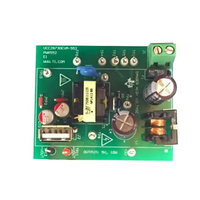
User's Guide
SLUUB75 – February 2015
Using the UCC28730EVM-552 10-W Adaptor Module With
PSR and Wake-Up Monitor
The UCC28730EVM-552 evaluation module is a 10-W off-line discontinuous mode (DCM) flyback
converter that provides constant-voltage (CV) and constant-current (CC) output regulation without the use
of an optical coupler. The controller uses primary-side regulation (PSR) and detects a wake-up signal from
the UCC24650 secondary-side voltage-droop monitor for improved transient response to large load steps.
The EVM demonstrates how the UCC28730 can provide ultra-low standby power without sacrificing startup time or output transient response with an internal 700-V start-up switch, dynamically controlled
operating states, and a tailored modulation profile. The UCC28730 uses frequency modulation, peak
primary current modulation, valley switching and valley skipping in its control algorithm in order to
maximize efficiency over the entire operating range.
1
2
3
4
5
6
7
Contents
Description .................................................................................................................... 2
1.1
Typical Applications ................................................................................................ 3
1.2
Features .............................................................................................................. 3
Electrical Performance Specifications ..................................................................................... 4
Schematic ..................................................................................................................... 5
Test Setup .................................................................................................................... 6
4.1
Test Equipment ..................................................................................................... 6
4.2
Recommended Test Setup ........................................................................................ 7
4.3
List of Test Points ................................................................................................... 8
4.4
Applying Power to the EVM ....................................................................................... 9
4.5
No-Load Power Consumption ..................................................................................... 9
4.6
Line/Load Regulation and Efficiency Measurement Procedure .............................................. 9
4.7
Output Voltage Ripple .............................................................................................. 9
4.8
Equipment Shutdown ............................................................................................. 10
Performance Data and Typical Characteristic Curves................................................................. 10
5.1
Efficiency ........................................................................................................... 10
5.2
No-Load Power Consumption ................................................................................... 11
5.3
Output Voltage vs Output Current .............................................................................. 11
5.4
Transient Response............................................................................................... 12
5.5
Output Ripple ...................................................................................................... 13
5.6
Turn On Waveform ................................................................................................ 14
5.7
Switching Waveform .............................................................................................. 15
5.8
EMI Dithering Waveform ......................................................................................... 16
5.9
ENS Function ...................................................................................................... 16
EVM Assembly Drawing and PCB Layout .............................................................................. 18
Bill of Materials ............................................................................................................. 20
List of Figures
1
UCC28730EVM-552 Schematic ........................................................................................... 5
2
UCC28730EVM-552 Recommended Test Set Up For No-Load Operation .......................................... 7
3
FUCC28730EVM-552 Recommended Test Set Up With Load ........................................................ 8
4
UCC28730EVM-552 Average Efficiency ................................................................................ 10
5
UCC28730EVM-552 Efficiency ........................................................................................... 10
6
UCC28730EVM-552 No-Load Power Consumption ................................................................... 11
SLUUB75 – February 2015
Submit Documentation Feedback
Using the UCC28730EVM-552 10-W Adaptor Module With PSR and WakeUp Monitor
Copyright © 2015, Texas Instruments Incorporated
1
�Description
www.ti.com
7
UCC28730EVM-552 Output Voltage as a Function of Load Current................................................ 11
8
FUCC28730EVM-552 Load Transient ................................................................................... 12
9
UCC28730EVM-552 WAKE Signal During Load Transient
10
UCC28730EVM-552 WAKE Signal Transmitted to the AUX Winding............................................... 13
11
Output Ripple ............................................................................................................... 13
12
Output Voltage Turn On Waveform ...................................................................................... 14
13
CS and DRV at Turn On
14
Primary-Side Switching Waveform ....................................................................................... 15
15
Secondary Side Switching Waveform ................................................................................... 15
16
EMI Dithering Waveform .................................................................................................. 16
17
ENS and SR Gate as Load Decreases.................................................................................. 16
18
ENS and SR GATE as Load Increases ................................................................................. 17
19
UCC28730EVM-552 Top Layer Assembly Drawing (Top view)
20
UCC28730EVM-552 Bottom Layer Assembly Drawing (Bottom view) .............................................. 18
21
UCC28730EVM-552 Top Copper (Top View) .......................................................................... 19
22
UCC28730EVM-552 Bottom Copper (Bottom View)
..........................................................
..................................................................................................
.....................................................
..................................................................
12
14
18
19
List of Tables
1
1
UCC28730EVM-552 Electrical Performance Specifications ........................................................... 4
2
Test Point Functional Description.......................................................................................... 8
3
Bill of Materials
.............................................................................................................
20
Description
This evaluation module uses the UCC28730 Constant-Voltage, Constant-Current Flyback Controller with
PSR and Wake-Up Monitoring with the UCC24650 200-V Wake-Up Monitor for Fast Transient PSR in a
10-W converter to provide 2 A of constant charge current. The input accepts a voltage range of 85 VAC to
265 VAC. The output is designed for 5 V when in constant voltage mode and will deliver 2 A of constant
current down to an output voltage of less than 2 V.
Depending upon the operating conditions, the control law algorithm will modulate the switching frequency
or the peak primary current to satisfy the power transfer requirements. As the load is increased from zero,
the converter will transition through a frequency modulation (FM) mode where the peak primary current is
held constant at one-third of its full-load peak value as the switching frequency increases from a minimum
value to maintain energy transfer up to 28 kHz. When the load is increased to the level at which the
switching frequency reaches 28 kHz, the controller will keep the switching frequency fixed and modulate
the amplitude of peak primary current, increasing it from one-third its peak value up to its maximum full
load peak current value; this area of operation is referred to as the amplitude modulation (AM) range.
Further increase in load demand will transition the controller into another frequency modulation mode
where the peak primary current is constant at its maximum designed value and the switching frequency is
increased, as needed, up to the controller’s maximum 83 kHz switching frequency.
Using PSR, the output voltage is indirectly sensed on the auxiliary winding at the end of the transfer of
stored transformer energy to the secondary to maintain a tightly regulated output. The Wake-Up
monitoring feature operates in conjunction with the secondary-side UCC24650 to allow light-load and noload switching frequencies to approach 32 Hz, minimizing no-load power consumption to less than 5 mW,
yet provide a fast dynamic response to load transients without requiring large output capacitance. The
controller will further enhance its efficient operation with valley switching. The UCC28730 also uses
dithering of the gate drive which helps to ease EMI compliance.
This user’s guide provides the schematic, component list, assembly drawing, art work, and test set up
necessary to evaluate the UCC28730 and UCC24650 in a typical off-line converter application.
2
Using the UCC28730EVM-552 10-W Adaptor Module With PSR and WakeUp Monitor
Copyright © 2015, Texas Instruments Incorporated
SLUUB75 – February 2015
Submit Documentation Feedback
�Description
www.ti.com
1.1
Typical Applications
The UCC28730 is suited for use in isolated off-line systems requiring minimal stand-by power, high
efficiency, and fault protection; applications such as:
• Adapters/chargers for smart phones, tablets, and consumer electronics
• TV and monitor power supplies
• SMPS for home appliance and building automation
• Housekeeping power supply
1.2
Features
The UCC28730EVM-552 features include:
• AC input range 85 VAC to 265 VAC
• DC output of 5 V, 2 A
• No-load stand-by power consumption less than 5 mW (“Zero-Power”)
• Wake-up detection for fast dynamic response
• Primary-side regulation eliminates opto-coupler
• ±5% output voltage regulation
• ±5% output current regulation
• Average efficiency > 83%; exceeds Level VI and CoC Tier 2 specifications, effective 2016
• Output overcurrent and short circuit protection
• Output overvoltage protection
• Input brown-out protection
• Auto re-start on fault
• Resonant ring valley switching operation for highest overall efficiency
• Frequency dither
• Internal 700-V start-up switch to start up the supply directly from the bulk rail
• 10% efficiency > 80%; complies with CoC Tier 2 specification
• Secondary-side synchronous rectification driven by UCC24610
WARNING
High voltage levels are present on the evaluation module whenever
it is energized. Proper precautions must be taken when working
with the EVM. The large bulk capacitors, C3 and C4, and the output
capacitors, C9 and C10, must be completely discharged before the
EVM can be handled. Serious injury can occur if proper safety
precautions are not followed.
SLUUB75 – February 2015
Submit Documentation Feedback
Using the UCC28730EVM-552 10-W Adaptor Module With PSR and WakeUp Monitor
Copyright © 2015, Texas Instruments Incorporated
3
�Electrical Performance Specifications
2
www.ti.com
Electrical Performance Specifications
Table 1. UCC28730EVM-552 Electrical Performance Specifications
Parameter
Test Conditions
MIN
NOM
MAX
UNIT
85
115/230
265
VRMS
0.250
ARMS
47
60/50
Input Characteristics
VIN
Voltage range
Maximum input current
VIN = VINmin, IOUT = IOUTmax
Line frequency
VINmin ≤ VIN ≤ VINmax, IOUT = 0 A
No-load power consumption
63
Hz
5
mW
Output Characteristics
VOUT
Output voltage, CV mode
VINmin ≤ VIN ≤ VINmax, 0 A ≤ IOUT ≤ IOUTmax
4.75
5
5.25
V
IOUTmax
Output load current, CV mode
VINmin ≤ VIN ≤ VINmax
1.95
2.05
2.15
A
Output voltage regulation
Line Regulation: VINmin ≤ VIN ≤ VINmax,
IOUT = IOUTmax
5
Load Regulation: 0A ≤ IOUT ≤ IOUTmax
5
Output voltage ripple
VINmin ≤ VIN ≤ VINmax, 0A ≤ IOUT ≤ IOUTmax
80
mVpp
Output over current,
VINmin ≤ VIN ≤ VINmax
2.15
A
Minimum output voltage, CC
mode
VINmin ≤ VIN ≤ VINmax, IOUT = IOCC
1.4
2
V
IOUT = IOUTmax
62
IOUT = 10% IOUTmax
34
IOCC
Brown-out protection
%
VRMS
Systems Characteristics
fSW
Switching frequency
0.05
Average efficiency
25%, 50%, 75%, 100% load average
84
10% efficiency
10% load
80
Operating temperature
4
50
%
25
Using the UCC28730EVM-552 10-W Adaptor Module With PSR and WakeUp Monitor
Copyright © 2015, Texas Instruments Incorporated
kHz
°C
SLUUB75 – February 2015
Submit Documentation Feedback
�Schematic
www.ti.com
3
Schematic
Figure 1 illustrates the UCC28730EVM-552 schematic.
DANGER HIGH VOLTAGE
L1
BU9H-103R25BL
10mH
TP7
BULK
3
T1
OUTPUT: 5V @ 2A MAX
9
TP4
-
D2
HD06-T
RT1
D4
MRA4007T3G
PGND
t°
8
TP9
SW
PGND
33
7508111120
C9
330uF
C10
330uF
R20
100k
C11
1 μF
SGND
TP12
VOUT-
J2
VOUT+
2
D+
3
D-
4
VOUT-
1,2,3
7,8
5,6,
R15
0
D1
U2
1
TP6
DRV
BAV21W-7-F
200V
C7
1 μF
D5
NF
R1
24.3
TP8
DRAIN
R5
100k
R8
U1
1
2
3
C2
2.2μF
R3
31.6k
R4
NF
4
VDD
HV
VDD
GND
ENSR
DRV
JMP1
GND
CS
3
R7
5
732
TP5
CS
R9
9.09
R11
1.96
R17
10.0
R18
10
R19
0
JMP2
U3
1
R6
0
6
R16
10.0
4
NC
2
CBC
5
WAKE
UCC24650DBV
Q1
STU7NM60N
5.11
8
VS
UCC28730D
R12
1.96
4
SYNC
EN/TOFF
VD
VS
TON
GND
VCC
GATE
8
7
6
TP10
SR GATE
5
UCC24610D
C5
27pF
R13
255k
TP3
PGND
PGND
2
3
R2
110k
TP2
VDD
C1
4.7μF
Q2
CSD18534Q5A
4
6
R10
TP1
VAUX
10 ohm
1
7
PGND
~
NEUTRAL
+
10
1
5
4
4
LINE
D3
SMBJ130A-13-F
C4
10μF
3
~
C3
10μF
J1
L2
1 μH
6
TP11
VOUT+
2
5
1
F1
277 VAC, 2 A
2
INPUT: 85 VRMS - 265 VRMS, 0.35 A PEAK, 47 Hz TO 63 Hz
PGND
R14
56.2k
C8
1uF
PGND
C6
680pF
NF = NOT FITTED
PGND
SGND
Figure 1. UCC28730EVM-552 Schematic
SLUUB75 – February 2015
Submit Documentation Feedback
Using the UCC28730EVM-552 10-W Adaptor Module With PSR and Wake-Up
Monitor
Copyright © 2015, Texas Instruments Incorporated
5
�Test Setup
4
www.ti.com
Test Setup
Figure 2 shows the equipment set up when measuring the input power consumption during no-load
operation. Note the addition of the 1-kΩ shunt resistor in Figure 2. During the no-load test, set the power
analyzer for long averaging mode in order to include several cycles of operation. Use an appropriate
current scale factor for the external shunt. Due to the extremely low measured values, placement of the
shunt is critical and should be positioned right at the input terminals of the EVM. Figure 3 shows the
recommended test equipment set up to evaluate the UCC28730EVM-552 with a load.
WARNING
High voltages that may cause injury exist on this evaluation
module (EVM). Please ensure all safety procedures are followed
when working on this EVM. Never leave a powered EVM
unattended.
4.1
Test Equipment
AC Voltage Source: For an input source, use an isolated variable AC source capable of supplying
between 85 VAC and 265 VAC at no less than 20 W and connected as shown in Figure 2 and Figure 3. For
accurate efficiency calculations, insert a power meter between the neutral line of the AC source and the
Neutral terminal of the EVM. For highest accuracy in loaded conditions, connect the voltage terminals of
the power meter directly across the Line and Neutral terminals of the EVM. For highest accuracy at noload, connect the V+ voltage terminal of the power meter at the Line terminal of the EVM and the V–
terminal of the power meter ahead of the shunt resistor (refer to Figure 2).
Output Load: Use a programmable electronic load capable of sinking 0 A to 3 A. For constant current
mode testing of the EVM, set the electronic load to constant resistance mode.
Power Meter: Use a power analyzer capable of measuring low input current, typically less than 1 mA, and
a long integration mode, when low power standby mode input power measurements are taken. An
example of such an analyzer is the Voltech PM100 Single Phase Power Analyzer. An external precision 1kΩ shunt, with a current scale factor of 100000 mV/A, was used. The power analyzer was set to
integration mode over 6 minutes for a reading of mW-hour in order to display one-tenth the averaged
results (refer to Figure 2).
Multimeters: For highest accuracy, VOUT can be monitored by connecting a DC voltmeter, DMM V1,
directly across the VOUT+, TP 11, and VOUT–, TP12, as shown in Figure 3. Place a DC current meter,
DMM A1, in series with the electronic load for accurate output current measurements.
Oscilloscope: A digital or analog oscilloscope with 500 MHz scope probes is recommended.
Fan: Forced air cooling is not required.
Recommended Wire Gauge: a minimum of 18-AWG wire is recommended. The wire connections
between the AC source and the EVM and the wire connections between the EVM and the load should be
less than two feet long.
6
Using the UCC28730EVM-552 10-W Adaptor Module With PSR and WakeUp Monitor
Copyright © 2015, Texas Instruments Incorporated
SLUUB75 – February 2015
Submit Documentation Feedback
�Test Setup
www.ti.com
4.2
Recommended Test Setup
POWER METER
AC SOURCE
+ - + VHI
VLO
AHI
ALO
Line
Neutral
AEXT
1k
Figure 2. UCC28730EVM-552 Recommended Test Set Up For No-Load Operation
SLUUB75 – February 2015
Submit Documentation Feedback
Using the UCC28730EVM-552 10-W Adaptor Module With PSR and WakeUp Monitor
Copyright © 2015, Texas Instruments Incorporated
7
�Test Setup
www.ti.com
AC SOURCE
Line
Neutral
POWER METER
+ - + VHI
VLO
AHI
ALO
AEXT
DMM A1
+
-
ELECTRONIC
LOAD
-
+
DMM V1
+
-
Oscilloscope
Figure 3. FUCC28730EVM-552 Recommended Test Set Up With Load
4.3
List of Test Points
Table 2. Test Point Functional Description
8
Test Point
Name
Description
TP1
VAUX
Auxiliary windings voltage
TP2
VDD
U1, pin 1 bias supply
TP3
PGND
Primary-side ground
TP4
PGND
Primary-side ground
TP5
CS
TP6
DRV
U1, pin 6 gate drive
TP7
BULK
Bulk input voltage
TP8
DRAIN
Q1 drain
TP9
SW
TP10
SR GATE
TP11
VOUT+
Positive output terminal of the EVM to the load
TP12
VOUT–
Return connection of the EVM output to the load
U1, pin 5 current sense
Switch node, WAKE signal
U3, pin 5 synchronous rectifier gate drive
Using the UCC28730EVM-552 10-W Adaptor Module With PSR and WakeUp Monitor
Copyright © 2015, Texas Instruments Incorporated
SLUUB75 – February 2015
Submit Documentation Feedback
�Test Setup
www.ti.com
4.4
Applying Power to the EVM
Use the following steps when applying power to the EVM:
1. Set up the EVM as shown in Figure 2 if testing at no-load, or Figure 3 if testing with a load.
2. If testing with a load, set the electronic load to constant resistance mode.
3. Set the AC source voltage between 85 VAC and 265 VAC.
4. Monitor the output voltage on DMM V1.
5. Monitor the output current on DMM A1.
4.5
No-Load Power Consumption
Use the following steps when testing no-load power consumption:
1. Use the test set up shown in Figure 2. Careful placement of the shunt resistor is required.
(a) Set the power analyzer to external shunt mode.
(b) Set the appropriate current scale factor for using an external shunt on the power analyzer. A 1-kΩ
shunt scales to 100000 mV/A, this is one-tenth the actual current scale factor that is needed for a
1-kΩ shunt but the value is limited by the Voltech PM100.
(c) Using integration mode for 6 minutes for mW-hour requires multiplying the readings by 10 to obtain
the input power consumption. Because the shunt must be scaled by one-tenth and the integration
requires a 10x factor, the combined result is that the no-load power can be read directly from the
power analyzer meter with this method.
2. Ramp up the input voltage to the EVM slowly (per Section 4.4), to avoid surge damage to the 1-kΩ
sense resistor.
3. Monitor the input power on the power analyzer while varying the input voltage.
4. Make sure the EVM is off and the bulk capacitors and output capacitors are completely discharged
before handling the EVM.
4.6
Line/Load Regulation and Efficiency Measurement Procedure
For line/load regulation and efficiency measurement, use the following steps:
1. For load regulation, use the test set up shown in Figure 3.
(a) Be sure to remove the external 1-kΩ shunt from the power analyzer and set the analyzer to normal
mode (not long averaging).
(b) Set the AC source to a constant voltage between 85 VAC and 265 VAC.
(c) Vary the load so that the output current varies from 0 A up to 2 A, as measured on DMM A1.
(d) Observe that the output voltage on DMM V1 remains within 5% of the 5-V constant voltage
regulation value.
(e) Observe that if the constant resistance level of the electronic load is decreased lower than the full
load value, the EVM will maintain constant current regulation within 5% of the programed value until
the output voltage drops below 2 V. The EVM will automatically restart once the constant resistance
load is increased.
2. For line regulation, use the test set up shown in Figure 3.
(a) Set the constant resistance load to sink the rated full load current.
(b) Vary the AC source from 85 VAC to 265 VAC.
(c) Observe that the output voltage on DMM V1 stays within 5% of the 5 V constant voltage regulation
value.
4.7
Output Voltage Ripple
Expose the ground barrel of the scope probe and place the tip of the probe on TP11, VOUT+, and rest the
exposed ground barrel of the probe on TP12, VOUT–, for output voltage ripple measurements.
SLUUB75 – February 2015
Submit Documentation Feedback
Using the UCC28730EVM-552 10-W Adaptor Module With PSR and WakeUp Monitor
Copyright © 2015, Texas Instruments Incorporated
9
�Test Setup
4.8
www.ti.com
Equipment Shutdown
1. To quickly discharge the output capacitors, make sure there is a load greater than 0 A on the EVM.
2. Turn off the AC source and wait for the bulk capacitors to discharge to a safe level.
5
Performance Data and Typical Characteristic Curves
Figure 4 through Figure 16 present typical performance curves and waveforms for UCC28730EVM-552.
5.1
Efficiency
The average efficiency at 115-VAC, 60-Hz nominal input and 230-VAC, 50-Hz nominal input exceeds the
0.84 design goal.
0.86
Efficiency Average
0.855
0.85
0.845
0.84
0.835
0.83
85
115
145
175
Input Voltage (VAC)
205
235
265
D001
Figure 4. UCC28730EVM-552 Average Efficiency
Figure 5 shows the actual measured efficiency with respect to load.
0.88
0.87
0.86
0.85
0.84
Efficiency
0.83
0.82
0.81
0.8
0.79
0.78
265 VAC, 50 Hz
230 VAC, 50 Hz
115 VAC, 60 Hz
85 VAC, 60 Hz
0.77
0.76
0.75
0
0.1
0.2
0.3
0.4
0.5
0.6
0.7
0.8
0.9
1
1.1
Load (A)
1.2
1.3
1.4
1.5
1.6
1.7
1.8
1.9
2
D002
Figure 5. UCC28730EVM-552 Efficiency
10
Using the UCC28730EVM-552 10-W Adaptor Module With PSR and WakeUp Monitor
Copyright © 2015, Texas Instruments Incorporated
SLUUB75 – February 2015
Submit Documentation Feedback
�Performance Data and Typical Characteristic Curves
www.ti.com
5.2
No-Load Power Consumption
No-load power consumption measured less than 4 mW over the entire line input range.
5
4.5
4
Input Power (mW)
3.5
3
2.5
2
1.5
1
0.5
0
85
135
185
Input Voltage (VAC)
235
265
D003
Figure 6. UCC28730EVM-552 No-Load Power Consumption
5.3
Output Voltage vs Output Current
In Figure 7, the converter is in constant-voltage operating mode from 0-A load up to approximately 2.1 A.
Once reaching this output over-current threshold, the converter transitions into constant-current mode
where the load current remains constant until the output voltage falls below 2 V, at which point the
converter shuts down. If the load demand is decreased to the constant current operating region, the
converter automatically re-starts.
6
Output Voltage (V)
5
4
3
2
265 VAC, 50 Hz
230 VAC, 50 Hz
115 VAC, 60 Hz
85 VAC, 60 Hz
1
0
0
0.5
1
1.5
2
Load Current (A)
2.5
D004
Figure 7. UCC28730EVM-552 Output Voltage as a Function of Load Current
SLUUB75 – February 2015
Submit Documentation Feedback
Using the UCC28730EVM-552 10-W Adaptor Module With PSR and WakeUp Monitor
Copyright © 2015, Texas Instruments Incorporated
11
�Performance Data and Typical Characteristic Curves
5.4
www.ti.com
Transient Response
The transient response shown in Figure 8 was taken with a 115-VAC, 60-Hz input voltage and a load
transition from 0 A to full load. Channel 4 is the load current on a scale of 1 A per division, channel 1 is
the output voltage on a scale of 200 mV per division, offset from the center line by –5.20 V. The cursors
show the undershoot from the regulated output voltage, under full load transient conditions. Output voltage
undershoot may vary dependent upon the specific time the transient occurs during the switching cycle.
Figure 8. FUCC28730EVM-552 Load Transient
Figure 9 shows the WAKE signal from the UCC24650 Wake-Up Monitor activating when the output
voltage falls below approximately 3% of its regulated value. Figure 10 shows the wake-up alert signal
transmitted to the PSR controller on the AUX winding.
Figure 9. UCC28730EVM-552 WAKE Signal During Load Transient
12
Using the UCC28730EVM-552 10-W Adaptor Module With PSR and WakeUp Monitor
Copyright © 2015, Texas Instruments Incorporated
SLUUB75 – February 2015
Submit Documentation Feedback
�Performance Data and Typical Characteristic Curves
www.ti.com
Figure 10. UCC28730EVM-552 WAKE Signal Transmitted to the AUX Winding
5.5
Output Ripple
Figure 11 shows the output voltage ripple, measured across TP11 and TP12 on the EVM. The
measurement was taken at full load with an input voltage of 115-VAC, 60-Hz and the waveform is AC
coupled, with 20-MHz bandwidth limit. The cursor indicates the maximum peak-to-peak limit of 80 mV
permitted for the design. The ripple pattern seen is characteristic of the EMI dithering method used by the
UCC28730 controller.
Figure 11. Output Ripple
SLUUB75 – February 2015
Submit Documentation Feedback
Using the UCC28730EVM-552 10-W Adaptor Module With PSR and WakeUp Monitor
Copyright © 2015, Texas Instruments Incorporated
13
�Performance Data and Typical Characteristic Curves
5.6
www.ti.com
Turn On Waveform
Figure 12 shows the output voltage at turn on under full load conditions with an input voltage of 115 VAC,
60 Hz.
Figure 12. Output Voltage Turn On Waveform
Figure 13 shows how the UCC28730 limits the first four switching-cycle current peaks to IPP(min) in order to
monitor for any initial input or output faults with limited power delivery. After these initial four pulses, the
controller will limit the amplitude of the peak primary current to approximately 0.67 × IPP(max). Modifications
are also made to DMAGCC, increasing it from 0.432 to 0.650. These modifications during startup allow high
frequency charge-up of the output capacitor to avoid audible noise. Once the VS signal is greater than
1.36 V (approximately 1.45 V on the output), DMAGCC is restored to its normal value and the peak primary
current resumes at IPP(max).
Figure 13. CS and DRV at Turn On
14
Using the UCC28730EVM-552 10-W Adaptor Module With PSR and WakeUp Monitor
Copyright © 2015, Texas Instruments Incorporated
SLUUB75 – February 2015
Submit Documentation Feedback
�www.ti.com
5.7
Performance Data and Typical Characteristic Curves
Switching Waveform
The typical switching waveform can be seen in Figure 14. Channel 1 shows the MOSFET drain-to-source
voltage at 100 V per division, channel 2 shows the AUX winding at 50 V per division, channel 3 is the CS
waveform at 500 mV per division, and channel 4 shows the gate drive at 10 V per division. The scan was
taken at 2-A load, 115-VAC, 60-Hz input voltage. At this operating point, the switching frequency is
dithering between 48 kHz and 40 kHz, due to valley skipping.
Figure 14. Primary-Side Switching Waveform
Figure 15 shows the switching waveforms on the secondary side, channel 1 is the SW node and channel
2 shows the UCC24610 gate drive for the secondary side synchronous rectifier.
Figure 15. Secondary Side Switching Waveform
SLUUB75 – February 2015
Submit Documentation Feedback
Using the UCC28730EVM-552 10-W Adaptor Module With PSR and WakeUp Monitor
Copyright © 2015, Texas Instruments Incorporated
15
�Performance Data and Typical Characteristic Curves
5.8
www.ti.com
EMI Dithering Waveform
The UCC28730 controller employs a unique control mechanism to help with EMI compliance. The DRV
pin drives the gate of the MOSFET with a sequence of pulses in which there are two longer pulses, two
medium pulses, and two shorter pulses at any operating point starting with the amplitude modulation
mode. The EMI dithering is not enabled at light load. Figure 16 shows the result of these varying pulse
widths on the CS signal, shown on channel 1. The medium length pulses are shown measured at 748 mV,
the longer pulses result in a peak current slightly greater, and the shorter pulses are slightly less. This
dithering adds to the frequency jitter caused by valley skipping and results in a spread spectrum for better
EMI compliance.
Figure 16. EMI Dithering Waveform
5.9
ENS Function
The ENS open-drain MOSFET output of the UCC24650 Wake-Up Monitor will disable the UCC24610
Synchronous Rectifier Driver when the load decreases below 0.03 A, as shown in Figure 17.
Figure 17. ENS and SR Gate as Load Decreases
16
Using the UCC28730EVM-552 10-W Adaptor Module With PSR and WakeUp Monitor
Copyright © 2015, Texas Instruments Incorporated
SLUUB75 – February 2015
Submit Documentation Feedback
�www.ti.com
Performance Data and Typical Characteristic Curves
The ENS re-enables the UCC24610 when the load increases above 0.09 A, as shown in Figure 18.
Controlling the secondary-side circuit during no-load and light-load conditions helps to reduce stand-by
and light-load power loss.
Figure 18. ENS and SR GATE as Load Increases
SLUUB75 – February 2015
Submit Documentation Feedback
Using the UCC28730EVM-552 10-W Adaptor Module With PSR and WakeUp Monitor
Copyright © 2015, Texas Instruments Incorporated
17
�EVM Assembly Drawing and PCB Layout
6
www.ti.com
EVM Assembly Drawing and PCB Layout
Figure 19 through Figure 22 show the design of the UCC28730EVM-552 printed circuit board. The final
dimensions of the single copper layer circuit measure 2.00 in by 2.40 in.
Figure 19. UCC28730EVM-552 Top Layer Assembly Drawing (Top view)
Figure 20. UCC28730EVM-552 Bottom Layer Assembly Drawing (Bottom view)
18
Using the UCC28730EVM-552 10-W Adaptor Module With PSR and WakeUp Monitor
Copyright © 2015, Texas Instruments Incorporated
SLUUB75 – February 2015
Submit Documentation Feedback
�EVM Assembly Drawing and PCB Layout
www.ti.com
Figure 21. UCC28730EVM-552 Top Copper (Top View)
Figure 22. UCC28730EVM-552 Bottom Copper (Bottom View)
SLUUB75 – February 2015
Submit Documentation Feedback
Using the UCC28730EVM-552 10-W Adaptor Module With PSR and WakeUp Monitor
Copyright © 2015, Texas Instruments Incorporated
19
�Bill of Materials
7
www.ti.com
Bill of Materials
The EVM components list shown in Table 3 according to the schematic shown in Figure 1.
Table 3. Bill of Materials
QTY
Designator
Description
Manufacturer
Part Number
1
C1
CAP, CERM, 4.7µF, 50V, ±10%, X5R, 0805
TDK
C2012X5R1H475K125AB
1
C2
CAP, CERM, 0.47µF, 50V, ±10%, X5R, 0805
Taiyo Yuden
UMK212BB7225KG-T
2
C3, C4
CAP, AL, 10 µF, 400 V, ±20%, TH
Nichicon
UCS2G100MPD1TD
1
C5
CAP, CERM, 27pF, 50V, ±5%, C0G/NP0, 0603
AVX
06035A270JAT2A
1
C6
CAP, CERM, 680 pF, 566 V, ±20%, CD, 7x11x7mm
TDK
CD65ZU2GA681MYNKA
3
C7, C8, C11
CAP, CERM, 1µF, 25V, ±10%, X7R, 0603
TDK
C1608X7R1E105K080AB
2
C9, C10
CAP, AL, 330µF, 6.3V, ±20%, 0.008 Ω, TH
Nichicon
RS80J331MDN1JT
1
D1
Diode, Switching, 200V, 0.2A, SOD-123
Diodes Inc.
BAV21W-7-F
1
D2
Diode, Switching-Bridge, 600 V, 0.8 A, MiniDIP
Diodes Inc.
HD06-T
1
D3
Diode, TVS, Uni, 130V, 600W, SMB
Diodes Inc.
SMBJ130A-13-F
1
D4
Diode, Standard Recovery Rectifier, 1000V, 1A, SMA
ON Semiconductor
MRA4007T3G
1
D5
Diode, Switching, 75V, 0.25A, SOD-323
Micro Commercial Components
1N4448WX-TP
1
F1
Fuse, 2 A, 250 V, TH
Bel Fuse Inc
RST 2
1
J1
Conn Term Block, 2POS, 5.08mm, TH
Phoenix Contact
1715721
1
J2
Connector, Receptable, USB Type A, Vertical, TH
CnC Tech
1002-021-01000
2
JMP1, JMP2
Jumper Wire, 200mil spacing, Red, pkg of 200
3M
923345-02-C
1
L1
Coupled inductor, 10mH, A, 3.5 Ω, TH
Coilcraft
BU9H-103R25BL
1
L2
Inductor, Shielded, Composite, 1 µH, 8.7 A, 13.25 mΩ, SMD
Coilcraft
XAL4020-102MEB
1
Q1
MOSFET, N-CH, 600V, 5A, IPAK
ST Microelectronics
STU7NM60N
1
Q2
MOSFET, N-CH, 60V, 50A, SON 5x6mm
Texas Instruments
CSD18534Q5A
1
R1
RES, 24.3 Ω, ±1%, 0.1 W, 0603
Yageo America
RC0603FR-0724R3L
1
R2
RES, 110kΩ, 1%, 0.1W, 0603
Vishay-Dale
CRCW0603110KFKEA
1
R3
RES, 31.6kΩ, 1%, 0.1W, 0603
Yageo America
RC0603FR-0731K6L
1
R4
RES, 16.0kΩ, 1%, 0.1W, 0603
Yageo America
RC0603FR-0716KL
1
R5
RES, 100kΩ, 1%, 0.25W, TH
Vishay-Dale
CMF50100K00FHEB
3
R6, R15, R19
RES, 0 Ω, ±5%, 0.1 W, 0603
Vishay-Dale
CRCW06030000Z0EA
1
R7
RES, 732 Ω, 1%, 0.1W, 0603
Yageo America
RC0603FR-07732RL
1
R8
RES, 5.11 Ω, 1%, 0.1W, 0603
Vishay-Dale
CRCW06035R11FKEA
1
R9
RES, 9.09 Ω, 1%, 0.1W, 0603
Vishay-Dale
CRCW06039R09FKEA
1
R10
RES, 33 Ω, 5%, 0.25W, 1206
Vishay-Dale
CRCW120633R0JNEA
2
R11, R12
RES, 1.96 Ω, 1%, 0.125W, 0805
Vishay-Dale
CRCW08051R96FKEA
1
R13
RES, 255k Ω, 1%, 0.1W, 0603
Vishay-Dale
CRCW0603255KFKEA
1
R14
RES, 56.2 k, 1%, 0.1 W, 0603
Vishay-Dale
CRCW060356K2FKEA
2
R16, R17
RES, 10.0 Ω, 1%, 0.1W, 0603
Vishay-Dale
CRCW060310R0FKEA
1
R18
RES, 10 Ω, 5%, 0.125W, 0805
Vishay-Dale
CRCW080510R0JNEA
1
R20
RES, 100kΩ, 5%, 0.1W, 0603
Vishay-Dale
CRCW0603100KJNEA
1
RT1
Thermistor NTC, 10 Ω, ±20%, Leaded
Ametherm
SL03 10001
1
T1
Tramformer, 667µH, TH
Wurth Elektronik eiSos
7508111120
10
TP1–TP10
Test Point, Multipurpose, White, TH
Keystone
5012
1
TP11
Test Point, Multipurpose, Red, TH
Keystone
5010
1
TP12
Test Point, Multipurpose, Black, TH
Keystone
5011
1
U1
Constant-Voltage Constant-Current Flyback Controller With PSR
and Wake-Up Monitoring, D0007A
Texas Instruments
UCC28730D
1
U2
Voltage Droop Monitor with Wake-Up Output, DBV0005A
Texas Instruments
UCC24650DBV
1
U3
GREEN Rectifier Controller Device, D0008A
Texas Instruments
UCC24610D
20
Using the UCC28730EVM-552 10-W Adaptor Module With PSR and WakeUp Monitor
Copyright © 2015, Texas Instruments Incorporated
SLUUB75 – February 2015
Submit Documentation Feedback
�STANDARD TERMS AND CONDITIONS FOR EVALUATION MODULES
1.
Delivery: TI delivers TI evaluation boards, kits, or modules, including any accompanying demonstration software, components, or
documentation (collectively, an “EVM” or “EVMs”) to the User (“User”) in accordance with the terms and conditions set forth herein.
Acceptance of the EVM is expressly subject to the following terms and conditions.
1.1 EVMs are intended solely for product or software developers for use in a research and development setting to facilitate feasibility
evaluation, experimentation, or scientific analysis of TI semiconductors products. EVMs have no direct function and are not
finished products. EVMs shall not be directly or indirectly assembled as a part or subassembly in any finished product. For
clarification, any software or software tools provided with the EVM (“Software”) shall not be subject to the terms and conditions
set forth herein but rather shall be subject to the applicable terms and conditions that accompany such Software
1.2 EVMs are not intended for consumer or household use. EVMs may not be sold, sublicensed, leased, rented, loaned, assigned,
or otherwise distributed for commercial purposes by Users, in whole or in part, or used in any finished product or production
system.
2
Limited Warranty and Related Remedies/Disclaimers:
2.1 These terms and conditions do not apply to Software. The warranty, if any, for Software is covered in the applicable Software
License Agreement.
2.2 TI warrants that the TI EVM will conform to TI's published specifications for ninety (90) days after the date TI delivers such EVM
to User. Notwithstanding the foregoing, TI shall not be liable for any defects that are caused by neglect, misuse or mistreatment
by an entity other than TI, including improper installation or testing, or for any EVMs that have been altered or modified in any
way by an entity other than TI. Moreover, TI shall not be liable for any defects that result from User's design, specifications or
instructions for such EVMs. Testing and other quality control techniques are used to the extent TI deems necessary or as
mandated by government requirements. TI does not test all parameters of each EVM.
2.3 If any EVM fails to conform to the warranty set forth above, TI's sole liability shall be at its option to repair or replace such EVM,
or credit User's account for such EVM. TI's liability under this warranty shall be limited to EVMs that are returned during the
warranty period to the address designated by TI and that are determined by TI not to conform to such warranty. If TI elects to
repair or replace such EVM, TI shall have a reasonable time to repair such EVM or provide replacements. Repaired EVMs shall
be warranted for the remainder of the original warranty period. Replaced EVMs shall be warranted for a new full ninety (90) day
warranty period.
3
Regulatory Notices:
3.1 United States
3.1.1
Notice applicable to EVMs not FCC-Approved:
This kit is designed to allow product developers to evaluate electronic components, circuitry, or software associated with the kit
to determine whether to incorporate such items in a finished product and software developers to write software applications for
use with the end product. This kit is not a finished product and when assembled may not be resold or otherwise marketed unless
all required FCC equipment authorizations are first obtained. Operation is subject to the condition that this product not cause
harmful interference to licensed radio stations and that this product accept harmful interference. Unless the assembled kit is
designed to operate under part 15, part 18 or part 95 of this chapter, the operator of the kit must operate under the authority of
an FCC license holder or must secure an experimental authorization under part 5 of this chapter.
3.1.2
For EVMs annotated as FCC – FEDERAL COMMUNICATIONS COMMISSION Part 15 Compliant:
CAUTION
This device complies with part 15 of the FCC Rules. Operation is subject to the following two conditions: (1) This device may not
cause harmful interference, and (2) this device must accept any interference received, including interference that may cause
undesired operation.
Changes or modifications not expressly approved by the party responsible for compliance could void the user's authority to
operate the equipment.
FCC Interference Statement for Class A EVM devices
NOTE: This equipment has been tested and found to comply with the limits for a Class A digital device, pursuant to part 15 of
the FCC Rules. These limits are designed to provide reasonable protection against harmful interference when the equipment is
operated in a commercial environment. This equipment generates, uses, and can radiate radio frequency energy and, if not
installed and used in accordance with the instruction manual, may cause harmful interference to radio communications.
Operation of this equipment in a residential area is likely to cause harmful interference in which case the user will be required to
correct the interference at his own expense.
SPACER
SPACER
SPACER
SPACER
SPACER
SPACER
SPACER
SPACER
�FCC Interference Statement for Class B EVM devices
NOTE: This equipment has been tested and found to comply with the limits for a Class B digital device, pursuant to part 15 of
the FCC Rules. These limits are designed to provide reasonable protection against harmful interference in a residential
installation. This equipment generates, uses and can radiate radio frequency energy and, if not installed and used in accordance
with the instructions, may cause harmful interference to radio communications. However, there is no guarantee that interference
will not occur in a particular installation. If this equipment does cause harmful interference to radio or television reception, which
can be determined by turning the equipment off and on, the user is encouraged to try to correct the interference by one or more
of the following measures:
•
•
•
•
Reorient or relocate the receiving antenna.
Increase the separation between the equipment and receiver.
Connect the equipment into an outlet on a circuit different from that to which the receiver is connected.
Consult the dealer or an experienced radio/TV technician for help.
3.2 Canada
3.2.1
For EVMs issued with an Industry Canada Certificate of Conformance to RSS-210
Concerning EVMs Including Radio Transmitters:
This device complies with Industry Canada license-exempt RSS standard(s). Operation is subject to the following two conditions:
(1) this device may not cause interference, and (2) this device must accept any interference, including interference that may
cause undesired operation of the device.
Concernant les EVMs avec appareils radio:
Le présent appareil est conforme aux CNR d'Industrie Canada applicables aux appareils radio exempts de licence. L'exploitation
est autorisée aux deux conditions suivantes: (1) l'appareil ne doit pas produire de brouillage, et (2) l'utilisateur de l'appareil doit
accepter tout brouillage radioélectrique subi, même si le brouillage est susceptible d'en compromettre le fonctionnement.
Concerning EVMs Including Detachable Antennas:
Under Industry Canada regulations, this radio transmitter may only operate using an antenna of a type and maximum (or lesser)
gain approved for the transmitter by Industry Canada. To reduce potential radio interference to other users, the antenna type
and its gain should be so chosen that the equivalent isotropically radiated power (e.i.r.p.) is not more than that necessary for
successful communication. This radio transmitter has been approved by Industry Canada to operate with the antenna types
listed in the user guide with the maximum permissible gain and required antenna impedance for each antenna type indicated.
Antenna types not included in this list, having a gain greater than the maximum gain indicated for that type, are strictly prohibited
for use with this device.
Concernant les EVMs avec antennes détachables
Conformément à la réglementation d'Industrie Canada, le présent émetteur radio peut fonctionner avec une antenne d'un type et
d'un gain maximal (ou inférieur) approuvé pour l'émetteur par Industrie Canada. Dans le but de réduire les risques de brouillage
radioélectrique à l'intention des autres utilisateurs, il faut choisir le type d'antenne et son gain de sorte que la puissance isotrope
rayonnée équivalente (p.i.r.e.) ne dépasse pas l'intensité nécessaire à l'établissement d'une communication satisfaisante. Le
présent émetteur radio a été approuvé par Industrie Canada pour fonctionner avec les types d'antenne énumérés dans le
manuel d’usage et ayant un gain admissible maximal et l'impédance requise pour chaque type d'antenne. Les types d'antenne
non inclus dans cette liste, ou dont le gain est supérieur au gain maximal indiqué, sont strictement interdits pour l'exploitation de
l'émetteur
3.3 Japan
3.3.1
Notice for EVMs delivered in Japan: Please see http://www.tij.co.jp/lsds/ti_ja/general/eStore/notice_01.page 日本国内に
輸入される評価用キット、ボードについては、次のところをご覧ください。
http://www.tij.co.jp/lsds/ti_ja/general/eStore/notice_01.page
3.3.2
Notice for Users of EVMs Considered “Radio Frequency Products” in Japan: EVMs entering Japan are NOT certified by
TI as conforming to Technical Regulations of Radio Law of Japan.
If User uses EVMs in Japan, User is required by Radio Law of Japan to follow the instructions below with respect to EVMs:
1.
2.
3.
Use EVMs in a shielded room or any other test facility as defined in the notification #173 issued by Ministry of Internal
Affairs and Communications on March 28, 2006, based on Sub-section 1.1 of Article 6 of the Ministry’s Rule for
Enforcement of Radio Law of Japan,
Use EVMs only after User obtains the license of Test Radio Station as provided in Radio Law of Japan with respect to
EVMs, or
Use of EVMs only after User obtains the Technical Regulations Conformity Certification as provided in Radio Law of Japan
with respect to EVMs. Also, do not transfer EVMs, unless User gives the same notice above to the transferee. Please note
that if User does not follow the instructions above, User will be subject to penalties of Radio Law of Japan.
SPACER
SPACER
SPACER
SPACER
SPACER
�【無線電波を送信する製品の開発キットをお使いになる際の注意事項】
本開発キットは技術基準適合証明を受けておりません。
本製品のご使用に際しては、電波法遵守のため、以下のいずれかの措置を取っていただく必要がありますのでご注意ください。
1.
2.
3.
電波法施行規則第6条第1項第1号に基づく平成18年3月28日総務省告示第173号で定められた電波暗室等の試験設備でご使用
いただく。
実験局の免許を取得後ご使用いただく。
技術基準適合証明を取得後ご使用いただく。
なお、本製品は、上記の「ご使用にあたっての注意」を譲渡先、移転先に通知しない限り、譲渡、移転できないものとします。
上記を遵守頂けない場合は、電波法の罰則が適用される可能性があることをご留意ください。
日本テキサス・インスツルメンツ株式会社
東京都新宿区西新宿6丁目24番1号
西新宿三井ビル
3.3.3
Notice for EVMs for Power Line Communication: Please see http://www.tij.co.jp/lsds/ti_ja/general/eStore/notice_02.page
電力線搬送波通信についての開発キットをお使いになる際の注意事項については、次のところをご覧くださ
い。http://www.tij.co.jp/lsds/ti_ja/general/eStore/notice_02.page
SPACER
4
EVM Use Restrictions and Warnings:
4.1 EVMS ARE NOT FOR USE IN FUNCTIONAL SAFETY AND/OR SAFETY CRITICAL EVALUATIONS, INCLUDING BUT NOT
LIMITED TO EVALUATIONS OF LIFE SUPPORT APPLICATIONS.
4.2 User must read and apply the user guide and other available documentation provided by TI regarding the EVM prior to handling
or using the EVM, including without limitation any warning or restriction notices. The notices contain important safety information
related to, for example, temperatures and voltages.
4.3 Safety-Related Warnings and Restrictions:
4.3.1
User shall operate the EVM within TI’s recommended specifications and environmental considerations stated in the user
guide, other available documentation provided by TI, and any other applicable requirements and employ reasonable and
customary safeguards. Exceeding the specified performance ratings and specifications (including but not limited to input
and output voltage, current, power, and environmental ranges) for the EVM may cause personal injury or death, or
property damage. If there are questions concerning performance ratings and specifications, User should contact a TI
field representative prior to connecting interface electronics including input power and intended loads. Any loads applied
outside of the specified output range may also result in unintended and/or inaccurate operation and/or possible
permanent damage to the EVM and/or interface electronics. Please consult the EVM user guide prior to connecting any
load to the EVM output. If there is uncertainty as to the load specification, please contact a TI field representative.
During normal operation, even with the inputs and outputs kept within the specified allowable ranges, some circuit
components may have elevated case temperatures. These components include but are not limited to linear regulators,
switching transistors, pass transistors, current sense resistors, and heat sinks, which can be identified using the
information in the associated documentation. When working with the EVM, please be aware that the EVM may become
very warm.
4.3.2
EVMs are intended solely for use by technically qualified, professional electronics experts who are familiar with the
dangers and application risks associated with handling electrical mechanical components, systems, and subsystems.
User assumes all responsibility and liability for proper and safe handling and use of the EVM by User or its employees,
affiliates, contractors or designees. User assumes all responsibility and liability to ensure that any interfaces (electronic
and/or mechanical) between the EVM and any human body are designed with suitable isolation and means to safely
limit accessible leakage currents to minimize the risk of electrical shock hazard. User assumes all responsibility and
liability for any improper or unsafe handling or use of the EVM by User or its employees, affiliates, contractors or
designees.
4.4 User assumes all responsibility and liability to determine whether the EVM is subject to any applicable international, federal,
state, or local laws and regulations related to User’s handling and use of the EVM and, if applicable, User assumes all
responsibility and liability for compliance in all respects with such laws and regulations. User assumes all responsibility and
liability for proper disposal and recycling of the EVM consistent with all applicable international, federal, state, and local
requirements.
5.
Accuracy of Information: To the extent TI provides information on the availability and function of EVMs, TI attempts to be as accurate
as possible. However, TI does not warrant the accuracy of EVM descriptions, EVM availability or other information on its websites as
accurate, complete, reliable, current, or error-free.
SPACER
SPACER
SPACER
SPACER
SPACER
SPACER
�SPACER
6.
Disclaimers:
6.1 EXCEPT AS SET FORTH ABOVE, EVMS AND ANY WRITTEN DESIGN MATERIALS PROVIDED WITH THE EVM (AND THE
DESIGN OF THE EVM ITSELF) ARE PROVIDED "AS IS" AND "WITH ALL FAULTS." TI DISCLAIMS ALL OTHER
WARRANTIES, EXPRESS OR IMPLIED, REGARDING SUCH ITEMS, INCLUDING BUT NOT LIMITED TO ANY IMPLIED
WARRANTIES OF MERCHANTABILITY OR FITNESS FOR A PARTICULAR PURPOSE OR NON-INFRINGEMENT OF ANY
THIRD PARTY PATENTS, COPYRIGHTS, TRADE SECRETS OR OTHER INTELLECTUAL PROPERTY RIGHTS.
6.2 EXCEPT FOR THE LIMITED RIGHT TO USE THE EVM SET FORTH HEREIN, NOTHING IN THESE TERMS AND
CONDITIONS SHALL BE CONSTRUED AS GRANTING OR CONFERRING ANY RIGHTS BY LICENSE, PATENT, OR ANY
OTHER INDUSTRIAL OR INTELLECTUAL PROPERTY RIGHT OF TI, ITS SUPPLIERS/LICENSORS OR ANY OTHER THIRD
PARTY, TO USE THE EVM IN ANY FINISHED END-USER OR READY-TO-USE FINAL PRODUCT, OR FOR ANY
INVENTION, DISCOVERY OR IMPROVEMENT MADE, CONCEIVED OR ACQUIRED PRIOR TO OR AFTER DELIVERY OF
THE EVM.
7.
USER'S INDEMNITY OBLIGATIONS AND REPRESENTATIONS. USER WILL DEFEND, INDEMNIFY AND HOLD TI, ITS
LICENSORS AND THEIR REPRESENTATIVES HARMLESS FROM AND AGAINST ANY AND ALL CLAIMS, DAMAGES, LOSSES,
EXPENSES, COSTS AND LIABILITIES (COLLECTIVELY, "CLAIMS") ARISING OUT OF OR IN CONNECTION WITH ANY
HANDLING OR USE OF THE EVM THAT IS NOT IN ACCORDANCE WITH THESE TERMS AND CONDITIONS. THIS OBLIGATION
SHALL APPLY WHETHER CLAIMS ARISE UNDER STATUTE, REGULATION, OR THE LAW OF TORT, CONTRACT OR ANY
OTHER LEGAL THEORY, AND EVEN IF THE EVM FAILS TO PERFORM AS DESCRIBED OR EXPECTED.
8.
Limitations on Damages and Liability:
8.1 General Limitations. IN NO EVENT SHALL TI BE LIABLE FOR ANY SPECIAL, COLLATERAL, INDIRECT, PUNITIVE,
INCIDENTAL, CONSEQUENTIAL, OR EXEMPLARY DAMAGES IN CONNECTION WITH OR ARISING OUT OF THESE
TERMS ANDCONDITIONS OR THE USE OF THE EVMS PROVIDED HEREUNDER, REGARDLESS OF WHETHER TI HAS
BEEN ADVISED OF THE POSSIBILITY OF SUCH DAMAGES. EXCLUDED DAMAGES INCLUDE, BUT ARE NOT LIMITED
TO, COST OF REMOVAL OR REINSTALLATION, ANCILLARY COSTS TO THE PROCUREMENT OF SUBSTITUTE GOODS
OR SERVICES, RETESTING, OUTSIDE COMPUTER TIME, LABOR COSTS, LOSS OF GOODWILL, LOSS OF PROFITS,
LOSS OF SAVINGS, LOSS OF USE, LOSS OF DATA, OR BUSINESS INTERRUPTION. NO CLAIM, SUIT OR ACTION SHALL
BE BROUGHT AGAINST TI MORE THAN ONE YEAR AFTER THE RELATED CAUSE OF ACTION HAS OCCURRED.
8.2 Specific Limitations. IN NO EVENT SHALL TI'S AGGREGATE LIABILITY FROM ANY WARRANTY OR OTHER OBLIGATION
ARISING OUT OF OR IN CONNECTION WITH THESE TERMS AND CONDITIONS, OR ANY USE OF ANY TI EVM
PROVIDED HEREUNDER, EXCEED THE TOTAL AMOUNT PAID TO TI FOR THE PARTICULAR UNITS SOLD UNDER
THESE TERMS AND CONDITIONS WITH RESPECT TO WHICH LOSSES OR DAMAGES ARE CLAIMED. THE EXISTENCE
OF MORE THAN ONE CLAIM AGAINST THE PARTICULAR UNITS SOLD TO USER UNDER THESE TERMS AND
CONDITIONS SHALL NOT ENLARGE OR EXTEND THIS LIMIT.
9.
Return Policy. Except as otherwise provided, TI does not offer any refunds, returns, or exchanges. Furthermore, no return of EVM(s)
will be accepted if the package has been opened and no return of the EVM(s) will be accepted if they are damaged or otherwise not in
a resalable condition. If User feels it has been incorrectly charged for the EVM(s) it ordered or that delivery violates the applicable
order, User should contact TI. All refunds will be made in full within thirty (30) working days from the return of the components(s),
excluding any postage or packaging costs.
10. Governing Law: These terms and conditions shall be governed by and interpreted in accordance with the laws of the State of Texas,
without reference to conflict-of-laws principles. User agrees that non-exclusive jurisdiction for any dispute arising out of or relating to
these terms and conditions lies within courts located in the State of Texas and consents to venue in Dallas County, Texas.
Notwithstanding the foregoing, any judgment may be enforced in any United States or foreign court, and TI may seek injunctive relief
in any United States or foreign court.
Mailing Address: Texas Instruments, Post Office Box 655303, Dallas, Texas 75265
Copyright © 2015, Texas Instruments Incorporated
spacer
�IMPORTANT NOTICE
Texas Instruments Incorporated and its subsidiaries (TI) reserve the right to make corrections, enhancements, improvements and other
changes to its semiconductor products and services per JESD46, latest issue, and to discontinue any product or service per JESD48, latest
issue. Buyers should obtain the latest relevant information before placing orders and should verify that such information is current and
complete. All semiconductor products (also referred to herein as “components”) are sold subject to TI’s terms and conditions of sale
supplied at the time of order acknowledgment.
TI warrants performance of its components to the specifications applicable at the time of sale, in accordance with the warranty in TI’s terms
and conditions of sale of semiconductor products. Testing and other quality control techniques are used to the extent TI deems necessary
to support this warranty. Except where mandated by applicable law, testing of all parameters of each component is not necessarily
performed.
TI assumes no liability for applications assistance or the design of Buyers’ products. Buyers are responsible for their products and
applications using TI components. To minimize the risks associated with Buyers’ products and applications, Buyers should provide
adequate design and operating safeguards.
TI does not warrant or represent that any license, either express or implied, is granted under any patent right, copyright, mask work right, or
other intellectual property right relating to any combination, machine, or process in which TI components or services are used. Information
published by TI regarding third-party products or services does not constitute a license to use such products or services or a warranty or
endorsement thereof. Use of such information may require a license from a third party under the patents or other intellectual property of the
third party, or a license from TI under the patents or other intellectual property of TI.
Reproduction of significant portions of TI information in TI data books or data sheets is permissible only if reproduction is without alteration
and is accompanied by all associated warranties, conditions, limitations, and notices. TI is not responsible or liable for such altered
documentation. Information of third parties may be subject to additional restrictions.
Resale of TI components or services with statements different from or beyond the parameters stated by TI for that component or service
voids all express and any implied warranties for the associated TI component or service and is an unfair and deceptive business practice.
TI is not responsible or liable for any such statements.
Buyer acknowledges and agrees that it is solely responsible for compliance with all legal, regulatory and safety-related requirements
concerning its products, and any use of TI components in its applications, notwithstanding any applications-related information or support
that may be provided by TI. Buyer represents and agrees that it has all the necessary expertise to create and implement safeguards which
anticipate dangerous consequences of failures, monitor failures and their consequences, lessen the likelihood of failures that might cause
harm and take appropriate remedial actions. Buyer will fully indemnify TI and its representatives against any damages arising out of the use
of any TI components in safety-critical applications.
In some cases, TI components may be promoted specifically to facilitate safety-related applications. With such components, TI’s goal is to
help enable customers to design and create their own end-product solutions that meet applicable functional safety standards and
requirements. Nonetheless, such components are subject to these terms.
No TI components are authorized for use in FDA Class III (or similar life-critical medical equipment) unless authorized officers of the parties
have executed a special agreement specifically governing such use.
Only those TI components which TI has specifically designated as military grade or “enhanced plastic” are designed and intended for use in
military/aerospace applications or environments. Buyer acknowledges and agrees that any military or aerospace use of TI components
which have not been so designated is solely at the Buyer's risk, and that Buyer is solely responsible for compliance with all legal and
regulatory requirements in connection with such use.
TI has specifically designated certain components as meeting ISO/TS16949 requirements, mainly for automotive use. In any case of use of
non-designated products, TI will not be responsible for any failure to meet ISO/TS16949.
Products
Applications
Audio
www.ti.com/audio
Automotive and Transportation
www.ti.com/automotive
Amplifiers
amplifier.ti.com
Communications and Telecom
www.ti.com/communications
Data Converters
dataconverter.ti.com
Computers and Peripherals
www.ti.com/computers
DLP® Products
www.dlp.com
Consumer Electronics
www.ti.com/consumer-apps
DSP
dsp.ti.com
Energy and Lighting
www.ti.com/energy
Clocks and Timers
www.ti.com/clocks
Industrial
www.ti.com/industrial
Interface
interface.ti.com
Medical
www.ti.com/medical
Logic
logic.ti.com
Security
www.ti.com/security
Power Mgmt
power.ti.com
Space, Avionics and Defense
www.ti.com/space-avionics-defense
Microcontrollers
microcontroller.ti.com
Video and Imaging
www.ti.com/video
RFID
www.ti-rfid.com
OMAP Applications Processors
www.ti.com/omap
TI E2E Community
e2e.ti.com
Wireless Connectivity
www.ti.com/wirelessconnectivity
Mailing Address: Texas Instruments, Post Office Box 655303, Dallas, Texas 75265
Copyright © 2015, Texas Instruments Incorporated
�