User Guide
SLUUAL8 – July 2013
Using the UCC28740EVM-525 10 W ConstantVoltage, Constant-Current Charger Adaptor
Module
User’s Guide
Literature Number: SLUUAL8
July, 2013
�SLUUAL8
Using the UCC28740EVM-525 10 W Constant-Voltage, Constant-Current Charger Adapter Module
PSS- High Performance Isolated
1
2
3
4
5
6
7
8
Contents
Introduction ..................................................................................................................................... 4
Description ...................................................................................................................................... 4
2.1 Typical Applications .................................................................................................................. 4
2.2 Features .................................................................................................................................... 5
Electrical Performance Specifications ......................................................................................... 6
Schematic ........................................................................................................................................ 7
Test Setup ....................................................................................................................................... 8
5.1 Test Equipment ......................................................................................................................... 8
5.2 Recommended Test Setup ....................................................................................................... 9
5.3 List of Test Points ................................................................................................................... 10
5.4 Applying Power to the EVM .................................................................................................... 11
5.5 No-Load Power Consumption ................................................................................................. 11
5.6 Line/Load Regulation and Efficiency Measurement Procedure .............................................. 11
5.7 Output Voltage Ripple ............................................................................................................. 12
5.8 Equipment Shutdown .............................................................................................................. 12
Performance Data and Typical Characteristic Curves .............................................................. 13
6.1 Efficiency ................................................................................................................................. 13
6.2 Load Regulation ...................................................................................................................... 14
6.3 Line Regulation ....................................................................................................................... 15
6.4 No-Load Power Consumption ................................................................................................. 15
6.5 Output Voltage vs Output Current ........................................................................................... 16
6.6 Control Law ............................................................................................................................. 17
6.7 Bode Plot ................................................................................................................................ 18
6.8 Transient Response ................................................................................................................ 19
6.9 Output Ripple .......................................................................................................................... 20
6.10 Turn On Waveform ................................................................................................................. 21
6.11 Switching Waveform ............................................................................................................... 22
6.12 EMI Dithering Waveform ......................................................................................................... 23
EVM Assembly Drawing and PCB layout ................................................................................... 23
Bill of Materials ............................................................................................................................. 28
Figures
Figure 1. UCC28740EVM-525 Schematic ......................................................................................... 7
Figure 2. UCC28740EVM-525 Recommended Test Set Up For No-Load Operation .................... 9
Figure 3. UCC28740EVM-525 Recommended Test Set Up With Load ........................................ 10
Figure 4. UCC28740EVM-525 Average Efficiency ......................................................................... 13
Figure 5. UCC28740EVM-525 Load Regulation ............................................................................. 14
Figure 6. UCC28740EVM-525 Line Regulation .............................................................................. 15
Figure 7. UCC28740EVM-525 No-Load Power Consumption ....................................................... 15
Figure 8. UCC28740EVM-525 Output Voltage as a Function of Load Current ........................... 16
Figure 9. UCC28740EVM-525 Control Law Showing Switching Frequency as a Function of
Load Current .................................................................................................................... 17
Figure 10. UCC28740EVM-525 Loop Response Gain and Phase .................................................. 18
�SLUUAL8
Figure 11.
Figure 12.
Figure 13.
Figure 14.
Figure 15.
Figure 16.
Figure 17.
Figure 18.
Figure 19.
UCC28740EVM-525 Load Transient ............................................................................... 19
Output Ripple ................................................................................................................... 20
Output voltage Turn On Waveform ................................................................................ 21
Switching Waveform ........................................................................................................ 22
EMI Dithering Waveform ................................................................................................. 23
UCC28740EVM-525 Top Layer Assembly Drawing (Top view) .................................... 24
UCC28740EVM-525 Bottom Layer Assembly Drawing (Bottom view) ........................ 25
UCC28740EVM-525 Top Copper (Top View) .................................................................. 26
UCC28740EVM-525 Bottom Copper (Bottom View) ...................................................... 27
Table 1.
Table 2.
Table 3.
Tables
UCC28740EVM-525 EVM-001 Electrical Performance Specifications ........................... 6
Test Point Functional Description .................................................................................. 10
The EVM components list according to the schematic shown in Figure 1 ................ 28
�SLUUAL8
1 Introduction
The UCC28740EVM-525 evaluation module is a 10 Watt off-line discontinuous mode (DCM) flyback
converter that provides constant-voltage (CV) and constant-current (CC) output regulation by using
an optical coupler for tight voltage regulation and improved the transient response to large load
steps and primary side control for accurate constant current regulation. The target application for this
converter design is USB adapters for consumer electronics. The UCC28740 uses frequency
modulation, peak primary current modulation, valley switching and valley skipping in its control
algorithm in order to maximize efficiency over the entire operating range.
2 Description
This evaluation module uses the UCC28740 Constant-Voltage, Constant-Current Flyback Controller
Using Opto-Coupled Feed-Back in a 10 W converter to provide 2 A of constant charge current. The
input accepts a voltge range of 85 VAC to 265 VAC. The output is designed for 5 V when in
constant voltage mode and will deliver 2.1 A of constant charge down to an output voltage of less
than 2 V. Depending upon the operating conditions, the control law algorithm will modulate the
switching frequency or the peak primary current to satisfy the power transfer requirements. As the
load is increased from zero, the converter will transition through a frequency modulation mode
where the peak primary current is held constant at one-quarter of its full-load peak value as the
switching frequency increases from a minimum value to maintain energy transfer up to 32 kHz.
When the load is increased to the level at which the switching frequency reaches 32 kHz, the
controller will keep the switching frequency fixed and modulate the peak primary current, increasing
it from one-quarter its peak value up to its maximum full load peak current value; this area of
operation is refered to as the amplitude modulation range. Further increase in load demand will
transition the controller into another frequency modulation mode where the peak primary current is
constant at its maximum designed value and the switching frequency is increased as needed, up to
the controller’s maximum 100 kHz switching frequency. Opto-coupled feed-back maintains a tightly
regulated output with fast dynamic response to load transients. The controller will further enhance
its efficient operation with valley switching. The UCC28740 also uses dithering of the gate drive
helps to ease EMI compliance.
This user’s guide provides the schematic, component list, assembly drawing, art work, and test set
up necessary to evaluate the UCC28740 in a typical off-line converter application.
2.1
Typical Applications
The UCC28740 is suited for use in isolated off-line systems requiring high efficiency and fault
protection features including:
USB-Compliant Adapters and Chargers for Consumer Electronics such as smart phones, tablet
computers, and cameras
Stand-by Supply for TV and Desktop
White Goods
�SLUUAL8
2.2
Features
The UCC28740EVM-525 features include:
AC Input Range 85 VAC to 265 VAC
DC Output of 5 V, 2.1 A
No-Load Power Consumption less than 20 mW
Opto-Coupled Feedback for Constant Voltage Regulation and Fast Dynamic Response
Primary Side Control for Tight Constant Current Performance
± 3% Output Volage Regulation
± 5% Output Current Regulation
Average Efficiency > 80%
Output Over Current and Short Circuit Protection
Output Over Voltage Protection
Input Brown-Out Protection
Auto Re-Start on Fault
Quasi-Resonant Valley Switching
Frequency Dither
Internal 700V Start-Up Switch to Start up the Supply Directly From the Bulk Rail
Caution
High voltage levels are present on the evaluation module whenever it is energized. Proper precautions
must be taken when working with the EVM. The large bulk capacitors, C3 and C4, and the output
capacitors, C8 and C10, must be completely discharged before the EVM can be handled. Serious injury
can occur if proper safety precautions are not followed.
�SLUUAL8
3 Electrical Performance Specifications
Table 1.
UCC28740EVM-525 EVM-001 Electrical Performance Specifications
PARAMETER
TEST CONDITIONS
MIN
NOM
MAX
UNITS
85
115/230
265
VRMS
47
60/50
Input Characteristics
Voltage range, VIN
Maximum input current
VIN = VINmin, IOUT = IOUTmax
Line frequency
No-load power
consumption
0.265
VINmin ≤ VIN ≤ VINmax, IOUT = 0A
ARMS
63
Hz
20
mW
Output Characteristics
Output voltage, VOUT
VINmin ≤ VIN ≤ VINmax, 0A ≤ IOUT ≤ IOUTmax
4.85
5
5.15
V
Output load current, CV
mode, IOUTmax
VINmin ≤ VIN ≤ VINmax
1.995
2.1
2.205
A
Line Regulation:
Output voltage regulation
VINmin ≤ VIN ≤ VINmax, IOUT = IOUTmax
Load Regulation: 0A ≤ IOUT ≤ IOUTmax
Output over current, IOCC
VINmin ≤ VIN ≤ VINmax, 0A ≤ IOUT ≤ IOUTmax
VINmin ≤ VIN ≤ VINmax
Minimum output voltage,
CC mode
VINmin ≤ VIN ≤ VINmax, IOUT = IOCC
Brown-out protection
IOUT = IOUTmax
Transient response
undershoot
IOUT = IOUTmax to 0A load transient
Transient response time
IOUT = IOUTmax to 0A load transient
Output voltage ripple
0.1
%
0.1
%
1.78
150
mVpp
2.5
A
2
V
68
VRMS
4.3
V
20
ms
71
kHz
Systems Characteristics
Switching frequency, fSW
Average efficiency
Operating temperature
1.2
25%, 50%, 75%, 100% load average at
nominal input voltages
81
%
25
ºC
�LINE
NEUTRAL
J1
2
1
10 ohm
t°
RT1
RST 2
F1
277 VAC, 2 A
UCC28740EVM-525 Schematic
PGND
TP1
C1
2.2 µF
D1
BAS21
-
C2
2.2 µF
24.3
R1
+
~
~
Figure 1.
R3
27.4k
R2
105k
D2
HD06-T
0
R5
R4
22.0k
C3
6.8 µF
4
3
2
1
GND
FB
VS
VDD
R6
0
PGND
C5
196k
R7
5
6
8
0.047 µF
CS
DRV
HV
JMP1
C4
6.8 µF
U1
UCC28740D
L1
220 µH
JMP2
1.27k
R9
0
R8
1.87
R11
1.87
R10
R12
49.9
D4
US1M-E3/61T
D3
SMBJ120A-13-F
PGND
LTV-817A
T1
560 µH
2
1
SGND
FLb
OUT
FLa
1 Do Not Populate
3
4
U2
5
3
4
2
1
C6
100 pF
BIAS
PRI
Q1
STU7NM60N
DANGER HIGH VOLTAGE
C7
1 µF
1
BAS16-7-F
D7
D6
SBR10U45SP5-13
D5
SBR10U45SP5-13
1
R13
1
C9
C8
270 µF
1
R14
L2
1 µH
SGND
C11
1 µF
C10
270 µF
R18 1
2700pF
C13
1
R17
0
JMP3
TL431AIDBZ
U3
C12
R16
1.00k
R15
1.50k
R20
42.2k
R19
42.2k
TP3
R21
49.9
TP2
SGND
TP4
C14
1 µF
1
2
3
4
OUTPUT: 5V, 2.1A MAX
5
6
INPUT: 100 VRMS - 265 VRMS, 0.3 A PEAK, 47 Hz TO 63 Hz
J2
TP5
TP6
C15
1 µF
-VOUT
NC
NC
+VOUT
SLUUAL8
4 Schematic
�SLUUAL8
5 Test Setup
Figure 2 shows the equipment set up when measuring the input power consumption during no-load
operation. Note the addition of the 10 Ω shunt resistor in Figure 2. During the no-load test, the
power analyzer should be set for long averging mode in order the include several cycles of operation
and an appropriate current scale factor for using the external shunt must be used. Figure 3 shows
the recommended test equipment set up to evaluate the UCC28740EVM-525 with a load.
Warning
High voltages that may cause injury exist on this evaluation module (EVM). Please ensure
all safety procedures are followed when working on this EVM. Never leave a powered EVM
unattended.
5.1
Test Equipment
AC Voltage Source: The input source shall be an isolated variable AC source capable of supplying
between 85 VAC and 265 VAC at no less than 20 W and connected as shown in Figures 2 and 3. For
accurate efficiency calculations, a power meter should be inserted between the neutral line of the
AC source and the Neutral terminal of the EVM. For highest accuracy, connect the voltage
terminals of the power meter directly across the Line and Neutral terminals of the EVM.
Output Load: A programmable electronic load capable of sinking 0 A to 3 A shall be used. For
constant current mode testing of the EVM, the electronic load should be set to constant resistance
mode.
Power Meter: A power analyzer shall be capable of measuring low input current, typically less than
10mA, and a long averaging mode, if low power standby mode input power measurements are to be
taken. An example of such an analyzer is the Voltech PM100 Single Phase Power Analyzer. An
external 10 Ω shunt, with a current scale factor of 10 A/V, was used at a high sample rate over an
extended period of time in order to display the averaged results (refer to Figure 2).
Multimeters: For highest accuracy, VOUT can be monitored by connecting a DC voltmeter, DMM V1,
directly across the +VOUT and –VOUT terminals as shown in Figure 2 and Figure 3. A DC current
meter, DMM A1, should be placed in series with the electronic load for accurate output current
measurements.
Oscilloscope: A digital or analog oscilloscope with 500 MHz scope probes is recommended.
Fan: Forced air cooling is not required.
Recommended Wire Gauge: a minimum of AWG 18 wire is recommended. The wire connections
between the AC source and the EVM, and the wire connections between the EVM and the load
should be less than two feet long.
�SLUUAL8
5.2
Recommended Test Setup
Figure 2.
UCC28740EVM-525 Recommended Test Set Up For No-Load Operation
�SLUUAL8
Figure 3.
5.3
UCC28740EVM-525 Recommended Test Set Up With Load
List of Test Points
Table 2.
TEST POINT
Test Point Functional Description
NAME
DESCRIPTION
TP1
PGND
Primary side power ground
TP2
+LOOP
Loop injection point, EVM output
TP3
-LOOP
Loop injection point
�SLUUAL8
5.4
TEST POINT
NAME
TP4
SGND
Secondary side ground
DESCRIPTION
TP5
+VOUT
Positive output terminal of the EVM to the load
TP6
-VOUT
Return connection of the EVM output to the load
Applying Power to the EVM
1. Set up the EVM as shown in Figure 2 if testing at no-load, or Figure 3 if testing with a load.
2. If testing with a load, set the electronic load to constant resistance mode.
3. Set the AC source voltage between 85 VAC and 265 VAC.
4. Monitor the output voltage on DMM V1.
5. Monitor the output current on DMM A1.
5.5
No-Load Power Consumption
1. Use the test set up shown in Figure 2.
a.
Set the power analyzer to external shunt mode.
b.
Set the appropriate current scale factor for using an external shunt on the power analyzer.
A 10 Ω shunt scales to 10,000 mV/A for the PM100 Voltech.
c.
Set the power analyzer for long averaging time to include several cycles of operation. The
PM100 Voltech used for this test data was set to a long averaging time of 30 for accurate
power consumption measurement.
2. Apply power to the EVM per section 5.4.
3. Monitor the input power on the power analyzer while varying thinput voltage.
4. Make sure the EVM is off and the bulk capacitors and output capacitors are completely
discharged before handling the EVM.
5.6
Line/Load Regulation and Efficiency Measurement Procedure
1.
For load regulation, use the test set up shown in Figure 3.
a.
Be sure to remove the exteranal 10 Ω shunt from the power analyzer and set the analyzer
to normal mode (not long averaging).
b.
Set the AC source to a constant voltage between 85 VAC and 265 VAC.
c.
Vary the load so that the output current varies from 0 A up to 2.1 A, as measured on DMM
A1.
d.
Observe that the output voltage on DMM V1 remains within 3% of the 5 V constant voltage
regulation value.
�SLUUAL8
e.
2.
5.7
Observe that if the constant resistance level of the electronic load is decreased lower than
the full load value, the EVM will maintain constant current regulation within 5% of the
programed value until the output voltge drops below 2 V. The EVM will automatically
restart once the constant resistance load is increased.
For line regulation, use the test set up shown in Figure 3
a.
Set the constant resistance load to sink the full load current, approximately 2.38 Ω.
b.
Vary the AC source from 85 VAC to 265 VAC
c.
Observe that the output voltage on DMM V1 stays within 3% of the 5 V constant voltage
regulation value.
Output Voltage Ripple
1. Expose the ground barrel of the scope probe and place the tip of the probe on TP5, +VOUT,
and rest the exposed ground barrel of the probe on TP6, -VOUT, for output voltage ripple
measurements.
5.8
Equipment Shutdown
1. To quickly discharge the output capacitors, make sure there is a load greater than 0 A on the
EVM.
2. Turn off the AC source.
�SLUUAL8
6 Performance Data and Typical Characteristic Curves
Figure 4 through 11 present typical performance curves for UCC28740EVM-525.
Efficiency
AVERAGE EFFICIENCY
EFFICIENCY
6.1
0.820
0.815
0.810
0.805
0.800
0.795
0.790
0.785
0.780
0.775
0.770
0.765
0.760
0.755
0.750
230
115
265
85
85
115
145
175
205
235
265
INPUT VOLTAGE (VAC)
Figure 4.
UCC28740EVM-525 Average Efficiency
The average efficiency at 115 VAC, 60 Hz nominal input and 230 VAC, 50 Hz nominal input exceeds
the 0.80 design goal. Further increases in efficiency could be achieved with a transformer made
with a custom core and designed to operate at lower switching frequency over the entire operating
range.
�SLUUAL8
Load Regulation
LOAD REGULATION
0.5
OUTPUT VOLTAGE REGULATION (%)
6.2
0.4
0.3
0.2
0.1
85
0
115
230
‐0.1
‐0.2
‐0.3
‐0.4
‐0.5
85
135
185
235
INPUT VOLTAGE (VAC)
Figure 5.
UCC28740EVM-525 Load Regulation
Figure 5 shows the actual measured load regulation exceeded the 3% design goal.
265
�SLUUAL8
6.3
Line Regulation
LINE REGULATION
OUTPUT VOLTAGE REGULATION (%)
0.5
0.4
0.3
0.2
0.1
0
‐0.1
‐0.2
‐0.3
‐0.4
‐0.5
0
10
20
30
40
50
60
70
80
90
PERCENT OF FULL LOAD (%)
Figure 6.
UCC28740EVM-525 Line Regulation
Figure 6 shows the actual measured line regulation exceeded the 3% design goal.
No-Load Power Consumption
NO‐LOAD POWER CONSUMPTION
20
18
16
INPUT POWER (mW)
6.4
14
12
10
8
6
4
2
0
85
115
145
175
205
235
INPUT VOLTAGE (VAC)
Figure 7.
UCC28740EVM-525 No-Load Power Consumption
265
100
�SLUUAL8
No load power consumption measured less than 20 mW over the entire line input range.
Output Voltage vs Output Current
OUTPUT VOLTAGE AS A FUNCTION OF LINE
AND LOAD
6
5.5
5
4.5
OUTPUT VOLTAGE (V)
6.5
4
3.5
3
2.5
2
1.5
1
0.5
0
0
0.5
1
1.5
2
2.5
LOAD CURRENT (A)
85 VAC, 60 Hz
Figure 8.
115 VAC, 60 Hz
230 VAC, 50 Hz
265 VAC, 50 Hz
UCC28740EVM-525 Output Voltage as a Function of Load Current
In Figure 8, the converter is in constant-voltage operating mode from 0 A load up to approximately
2.2 A. Once reaching this output over-current threshold, the converter transitions into constantcurrent mode where the load current remains constant until the output voltge falls below 2 V, at
which point the converter shuts down. If the load demand is decreased to the constant current
operating region, the converter will automatically re-start.
�SLUUAL8
6.6
Control Law
CONTROL LAW in CV MODE
100
SWITCHING FREQUENCY (kHz)
90
80
70
60
50
40
30
20
10
0
0
0.3
0.6
0.9
1.2
1.5
1.8
2.1
LOAD CURRENT (A)
120VDC
Figure 9.
163VDC
325VDC
375VDC
UCC28740EVM-525 Control Law Showing Switching Frequency as a Function of Load
Current
As the load increases, the UCC28740 will transition from a frequency modulation mode at light load,
where the peak primary current is fixed at ¼ of its maximum programmed value, into a 32 kHz fixed
frequency, peak current amplitude modulation mode. Further increase in load will force a transition
into another frequency modulation mode where the peak primary side current is fixed at its peak
programmed value and the frequency will increase from 32 kHz up to the maimum frequency
required for energy transfer. The maximum designed switching frequency for this module is 71 kHz.
For ease in measuring the switching frequency, the data was taken with a DC input voltage. This
reduced the frequency dithering to only the controller’s EMI dithering scheme and limited the valley
skipping that would have been a result of the line frequency modulating the AC input.
�SLUUAL8
Bode Plot
60
180
30
90
0
0
‐30
‐90
‐60
10
100
1000
PHASE (degrees)
GAIN (dB)
6.7
‐180
10000
FREQUENCY (Hz)
GAIN (dB)
PHASE (degrees)
Figure 10. UCC28740EVM-525 Loop Response Gain and Phase
The gain, phase plot was measured with an AP Instruments Inc. Model 200 analog network
analyzer. The loop result was obtained by inserting a 200mV AC signal across TP2 and TP3. The
crossover frequency, with a 115 VAC, 60 Hz input and load current of 2 A, measured 1.38 kHz with a
phase margin of 71 degrees.
�SLUUAL8
6.8
Transient Response
Figure 11. UCC28740EVM-525 Load Transient
The transient response shown in Figure 11 was taken with a 115 VAC, 60 Hz input voltage and a
load transition from 0 A to full load. Channel 1 is the load current on a scale of 1 A per division,
channel 4 is the otutput voltage on a scale of 1 V per division. The cursor shows the minimum
acceptable voltage limit, 4.30 V, under transient conditions. Also note that the output waveform was
taken with the probe on TP5 with the ground referenced to TP4 but not using the tip and barrel
technique accounting for the high frequency noise seen on the waveform.
�SLUUAL8
6.9
Output Ripple
Figure 12. Output Ripple
Figure 12 shows the output voltage ripple, measured using tip and barrel across TP5 and TP6 on
the EVM. The measurement was taken at full load with an input voltage of 85 VAC, 60 Hz and the
waveform is AC coupled. The cursor shows the maximum peak to peak limit permitted for the
design.
�SLUUAL8
6.10 Turn On Waveform
Figure 13. Output voltage Turn On Waveform
Figure 13 shows the output voltage at turn on under full load conditions with an input voltage of 115
VAC, 60 Hz. The maximum voltage at the output was measured to be 5.12 VDC.
�SLUUAL8
6.11 Switching Waveform
Figure 14. Switching Waveform
The typical switching waveform can be seen inFigure 14. Channel 1 shows the VS pin at 2 V per
division and channel 2 shows the MOSFET drain to source voltage at 100 V per division. The scan
was taken at 1.8 A load, 115 VAC, 60 Hz input voltage. At this operating point, the switching
frequency is dithering between 58.8 kHz and 52.6 kHz due to valley skipping.
�SLUUAL8
6.12 EMI Dithering Waveform
Figure 15. EMI Dithering Waveform
The UCC28740 controller employs a unique control mechanism to help with EMI compliance. As
shown in Figure 15, the DRV pin, shown as channel 3, drives the gate of the MOSFET with a
sequence of pulses in which there will be two longer pulses, two medium pulses, and two shorter
pulses at any operating point starting with the amplitude modulation mode. The EMI dithering is not
enabled at light load. Figure 15 shows the result of these varying pulse widths on the CS signal,
shown on channel 4. The longer pulses result in a peak current threshold of 808 mV, the medium
length pulses are shown measured at 780 mV, and the shorter pulses measure a threshold voltage
of 752 mV. This dithering adds to the frequency jitter caused by valley skipping and results in a
spread spectrum for better EMI compliance.
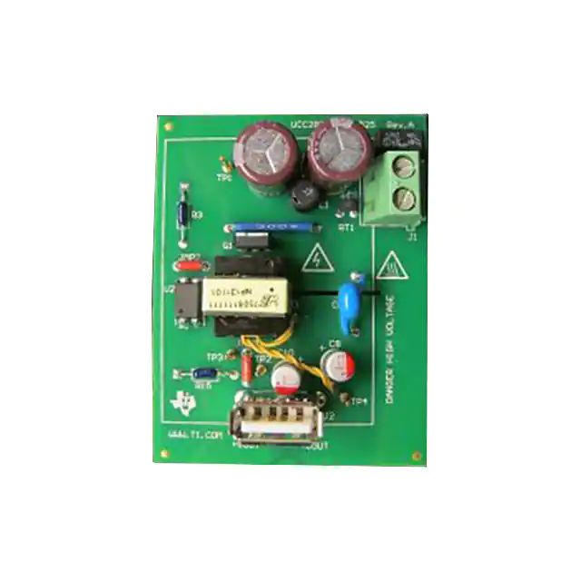
7 EVM Assembly Drawing and PCB layout
The following figures (Figure 16 through Figure 19) show the design of the UCC28740EVM-525
printed circuit board. The final dimensions of the single copper layer circuit measure 50.93 mm by
37.36 mm and the height is dominated by the USB connector at 18.4 mm.
�SLUUAL8
Figure 16. UCC28740EVM-525 Top Layer Assembly Drawing (Top view)
�SLUUAL8
Figure 17. UCC28740EVM-525 Bottom Layer Assembly Drawing (Bottom view)
�SLUUAL8
Figure 18. UCC28740EVM-525 Top Copper (Top View)
�SLUUAL8
Figure 19. UCC28740EVM-525 Bottom Copper (Bottom View)
�SLUUAL8
8 Bill of Materials
Table 3.
QTY
REFDES
The EVM components list according to the schematic shown in Figure 1
DESCRIPTION
MFR
PART NUMBER
2 C1, C2
CAP, CERM, 2.2 µF, 50 V, X7R, ±10%, 0805
Taiyo Yuden
UMK212BB7225KG‐T
2 C3, C4
CAP, ALUM, 6.8 µF, 400 V, ±20%, 110 mA, Radial
United Chemi‐Con
EKXG401ELL6R8MJ16S
1 C5
CAP, CERM, 0.047 µF, 25 V, X7R, ±5%, 0603
AVX
06033C473JAT2A
1 C6
CAP, CERM, 100 pF, 250 V, X1Y2, ±10%, Radial, Disc
TDK Corporation
CD70‐B2GA101KYNS
C7, C11,
4 C14, C15
CAP, CERM, 1 µF, 16 V, ±10%, X7R, 0603
TDK
C1608X7R1C105K
2 C8, C10
CAP, ALUM, 270 µF, 6.3 V, ±20%, 11 mΩ ESR, Radial
Nichicon
RNE0J271MDS1
0 C9
CAP, CERM, 1 µF, 16 V, ±10%, X7R, 0603
TDK
C1608X7R1C105K
0 C12
CAP, CERM, 4700 pF, 100 V, ±5%, X7R, 0603
AVX
06031C472JAT2A
1 C13
CAP, CERM, 2700 pF, 100 V, +/‐5%, X7R, 0603
AVX
06031C272JAT2A
1 D1
Diode, Switching, 200 V, 250 mA, SOD‐323
Infineon
Technologies
BAS 21‐03W E6327
1 D2
Diode, Switching‐Bridge, 600 V, 0.8 A, MiniDIP
Diodes Inc.
HD06‐T
1 D3
Diode, Transient Voltage Suppressor, 600 W, 120 V,
SMB
Diodes Inc
SMBJ120A‐13‐F
1 D4
Diode, Ultra Fast, 1000 V, 1 A, SMA
Vishay
Semiconductor
Diodes Division
US1M‐E3/61T
2 D5, D6
Diode, Super Barrier Rectifier, 45 V, 10 A, PowerDI5
Diodes Inc.
SBR10U45SP5‐13
0 D7
Diode, Ultrafast, 75 V, 0.3 A, SOT‐23
Diodes Inc.
BAS16‐7‐F
1 F1
Fuse, 2 A, 250 V, TH, 8.35 x 7.7 x 4 mm
Bel Fuse Inc
RST 2
1 J1
Conn, Term Block, 2POS, 5.08 mm, TH
Phoenix Contact
1715721
1 J2
Connector, Receptable, USB Type A, Vertical, TH
CnC Tech
1002‐021‐01000
1 JMP1
Jumper, 0.600 inch length, PVC Insulation, AWG 22
3M
923345‐06‐C
JMP2,
2 JMP3
Jumper, 0.200 inch length, PVC Insulation, AWG 22
3M
923345‐02‐C
1 L1
Inductor, RF Choke, 220 µH, ± 10%, 6 mm Dia.
Wurth Electronics
Inc
7447462221
1 L2
Inductor, Shielded, Composite, 1 µH, 8.7 A, 13.25 mΩ,
SMD, 4 mm x 2.1 mm x 4 mm
Coilcraft
XAL4020‐102MEB
1 Q1
MOSFET, N‐CH, 600 V, 5 A, 0.9 Ω, TO251‐3
STMicroelectronics
STU7NM60N
1 R1
RES, 24.3 Ω, ±1%, 0.1 W, 0603
Yageo America
RC0603FR‐0724R3L
1 R2
RES, 105 kΩ, ±1%, 0.1 W, 0603
Vishay‐Dale
CRCW0603105KFKEA
1 R3
RES, 27.4 kΩ, ±1%, 0.25 W, TH
Vishay‐Dale
CMF5027K400FHEB
1 R4
RES, 22.0 kΩ, ±1%, 0.1 W, 0603
Yageo America
RC0603FR‐0722KL
1 R5
RES, 0 Ω, ±5%, 0.125 W, 0805
Vishay‐Dale
CRCW08050000Z0EA
Vishay‐Dale
CRCW06030000Z0EA
3 R6, R8, R17 RES, 0 Ω, ±5%, 0.1 W, 0603
�SLUUAL8
QTY
REFDES
DESCRIPTION
MFR
PART NUMBER
1 R7
RES, 196 kΩ, ±1%, 0.1 W, 0603
Yageo America
RC0603FR‐07196KL
1 R9
RES, 1.27 kΩ, ±1%, 0.1 W, 0603
Vishay‐Dale
CRCW06031K27FKEA
2 R10, R11
RES, 1.87 Ω, ±1%, 0.125 W, 0805
Vishay‐Dale
CRCW08051R87FKEA
1 R12
RES, 49.9 Ω, ±1%, 0.25 W, 1206
Vishay‐Dale
CRCW120649R9FKEA
0 R13
RES, 820 Ω, ±1%, 0.1 W, 0603
Yageo America
RC0603FR‐07820RL
0 R14
RES, 2.00 kΩ, ±1%, 0.1 W, 0603
Vishay‐Dale
CRCW06032K00FKEA
1 R15
RES, 1.50 kΩ, ±1%, 0.25 W, TH
Vishay‐Dale
CMF501K5000FHEB
1 R16
RES, 1.00 kΩ, ±1%, 0.1 W, 0603
Yageo America
RC0603FR‐071KL
0 R18
RES, 140 kΩ, ±1%, 0.1 W, 0603
Vishay‐Dale
CRCW0603140KFKEA
2 R19, R20
RES, 42.2 kΩ, ±1%, 0.1 W, 0603
Vishay‐Dale
CRCW060342K2FKEA
1 R21
RES, 49.9 Ω, ±1%, 0.1 W, 0603
Yageo America
RC0603FR‐0749R9L
1 RT1
Thermistor NTC, 10 Ω, ±20%, Leaded
Ametherm
SL03 10001
1 T1
Transformer, 560 µH, TH, 580 mil x 600 mil x 580 mil
Wurth Elektronik
eiSos
7508111111 Rev 001
TP1, TP2,
TP3, TP4,
6 TP5, TP6
Pin, Thru Hole, Tin Plate, for 0.062 PCB's
Vector
K24C/M
1 U1
Constant‐Voltage, Constant‐Current Flyback Controller
Using Opto‐Coupler Feedback, D0007A
Texas Instruments
UCC28740D
1 U2
Opto‐Isolator, 1 Channel, TH, DIP‐4
Lite‐On
LTV‐817A
1 U3
IC, Precision Adjustable Shunt Regulator, ±1%, SOT23‐3
Texas Instruments
TL431AIDBZ
�EVALUATION BOARD/KIT/MODULE (EVM) WARNINGS, RESTRICTIONS AND DISCLAIMER
For Feasibility Evaluation Only, in Laboratory/Development Environments. The EVM is not a complete product. It is intended solely for use for
preliminary feasibility evaluation in laboratory / development environments by technically qualified electronics experts who are familiar with the dangers
and application risks associated with handling electrical / mechanical components, systems and subsystems. It should not be used as all or part of a
production unit.
Your Sole Responsibility and Risk. You acknowledge, represent and agree that:
1.
You have unique knowledge concerning Federal, State and local regulatory requirements (including but not limited to Food and Drug
Administration regulations, if applicable) which relate to your products and which relate to your use (and/or that of your employees, affiliates,
contractors or designees) of the EVM for evaluation, testing and other purposes.
2.
You have full and exclusive responsibility to assure the safety and compliance of your products with all such laws and other
applicable regulatory requirements, and also to assure the safety of any activities to be conducted by you and/or your employees, affiliates,
contractors or designees, using the EVM. Further, you are responsible to assure that any interfaces (electronic and/or mechanical) between the
EVM and any human body are designed with suitable isolation and means to safely limit accessible leakage currents to minimize the risk of
electrical shock hazard.
3.
Since the EVM is not a completed product, it may not meet all applicable regulatory and safety compliance standards (such as UL, CSA, VDE,
CE, RoHS and WEEE) which may normally be associated with similar items. You assume full responsibility to determine and/or assure
compliance with any such standards and related certifications as may be applicable. You will employ reasonable safeguards to ensure that your
use of the EVM will not result in any property damage, injury or death, even if the EVM should fail to perform as described or expected.
Certain Instructions. Exceeding the specified EVM ratings (including but not limited to 85 VAC to 265 VAC input and 5 V output voltage, 2.5 A current,
10.5 W power, and 25 C environmental ranges) may cause property damage, personal injury or death. If there are questions concerning these ratings please
contact a TI field representative prior to connecting interface electronics including input power and intended loads. Any loads applied outside of the
specified output range may result in unintended and/or inaccurate operation and/or possible permanent damage to the EVM and/or interface electronics.
Please consult the EVM User’s Guide prior to connecting any load to the EVM output. If there is uncertainty as to the load specification, please contact a TI
field representative. During normal operation, some circuit components may have case temperatures greater than 60°C as long as the input and output ranges
are maintained at nominal ambient operating temperature. These components include but are not limited to linear regulators, switching transistors, pass
transistors, and current sense resistors which can be indentified using the EVM schematic located in the EVM User’s Guide. When placing measurement
probes near these devices during normal operation, please be aware that these devices may be very warm to the touch.
Agreement to Defend, Indemnify and Hold Harmless. You agree to defend, indemnify and hold TI, its licensors and their representatives harmless from
and against any and all claims, damages, losses, expenses, costs and liabilities (collectively, “Claims”) arising out of or in connection with any use of the
EVM that is not in accordance with the terms of this agreement. This obligation shall apply whether Claims arise under the law of tort or contract or any
other legal theory, and even if the EVM fails to perform as described or expected.
Safety-Critical or Life-Critical Applications. If you intend to evaluate TI components for possible use in safety-critical applications (such as life support)
where a failure of the TI product would reasonably be expected to cause severe personal injury or death, such as devices which are classified as FDA Class
III or similar classification, then you must specifically notify TI of such intent and enter into a separate Assurance and Indemnity Agreement.
�IMPORTANT NOTICE
Texas Instruments Incorporated and its subsidiaries (TI) reserve the right to make corrections, modifications, enhancements, improvements, and other
changes to its products and services at any time and to discontinue any product or service without notice. Customers should obtain the latest relevant
information before placing orders and should verify that such information is current and complete. All products are sold subject to TI’s terms and conditions
of sale supplied at the time of order acknowledgment.
TI warrants performance of its hardware products to the specifications applicable at the time of sale in accordance with TI’s standard warranty. Testing and
other quality control techniques are used to the extent TI deems necessary to support this warranty. Except where mandated by government requirements,
testing of all parameters of each product is not necessarily performed.
TI assumes no liability for applications assistance or customer product design. Customers are responsible for their products and applications using TI
components. To minimize the risks associated with customer products and applications, customers should provide adequate design and operating safeguards.
TI does not warrant or represent that any license, either express or implied, is granted under any TI patent right, copyright, mask work right, or other TI
intellectual property right relating to any combination, machine, or process in which TI products or services are used. Information published by TI regarding
third-party products or services does not constitute a license from TI to use such products or services or a warranty or endorsement thereof. Use of such
information may require a license from a third party under the patents or other intellectual property of the third party, or a license from TI under the patents
or other intellectual property of TI.
Reproduction of TI information in TI data books or data sheets is permissible only if reproduction is without alteration and is accompanied by all associated
warranties, conditions, limitations, and notices. Reproduction of this information with alteration is an unfair and deceptive business practice. TI is not
responsible or liable for such altered documentation. Information of third parties may be subject to additional restrictions.
Resale of TI products or services with statements different from or beyond the parameters stated by TI for that product or service voids all express and any
implied warranties for the associated TI product or service and is an unfair and deceptive business practice. TI is not responsible or liable for any such
statements.
TI products are not authorized for use in safety-critical applications (such as life support) where a failure of the TI product would reasonably be expected to
cause severe personal injury or death, unless officers of the parties have executed an agreement specifically governing such use. Buyers represent that they
have all necessary expertise in the safety and regulatory ramifications of their applications, and acknowledge and agree that they are solely responsible for
all legal, regulatory and safety-related requirements concerning their products and any use of TI products in such safety-critical applications,
notwithstanding any applications-related information or support that may be provided by TI. Further, Buyers must fully indemnify TI and its representatives
against any damages arising out of the use of TI products in such safety-critical applications.
TI products are neither designed nor intended for use in military/aerospace applications or environments unless the TI products are specifically designated
by TI as military-grade or "enhanced plastic." Only products designated by TI as military-grade meet military specifications. Buyers acknowledge and agree
that any such use of TI products which TI has not designated as military-grade is solely at the Buyer's risk, and that they are solely responsible for
compliance with all legal and regulatory requirements in connection with such use.
TI products are neither designed nor intended for use in automotive applications or environments unless the specific TI products are designated by TI as
compliant with ISO/TS 16949 requirements. Buyers acknowledge and agree that, if they use any non-designated products in automotive applications, TI will
not be responsible for any failure to meet such requirements.
Following are URLs where you can obtain information on other Texas Instruments products and application solutions:
Products
Amplifiers
Data Converters
DSP
Clocks and Timers
Interface
Logic
Power Mgmt
Microcontrollers
RFID
RF/IF and ZigBee® Solutions
amplifier.ti.com
dataconverter.ti.com
dsp.ti.com
www.ti.com/clocks
interface.ti.com
logic.ti.com
power.ti.com
microcontroller.ti.com
www.ti-rfid.com
www.ti.com/lprf
Applications
Audio
Automotive
Broadband
Digital Control
Medical
Military
Optical Networking
Security
Telephony
Video & Imaging
Wireless
www.ti.com/audio
www.ti.com/automotive
www.ti.com/broadband
www.ti.com/digitalcontrol
www.ti.com/medical
www.ti.com/military
www.ti.com/opticalnetwork
www.ti.com/security
www.ti.com/telephony
www.ti.com/video
www.ti.com/wireless
Mailing Address: Texas Instruments, Post Office Box 655303, Dallas, Texas 75265
Copyright © 2008, Texas Instruments Incorporated
�